WO2022014419A1 - Connecteur optique et module de connecteur optique - Google Patents
Connecteur optique et module de connecteur optique Download PDFInfo
- Publication number
- WO2022014419A1 WO2022014419A1 PCT/JP2021/025518 JP2021025518W WO2022014419A1 WO 2022014419 A1 WO2022014419 A1 WO 2022014419A1 JP 2021025518 W JP2021025518 W JP 2021025518W WO 2022014419 A1 WO2022014419 A1 WO 2022014419A1
- Authority
- WO
- WIPO (PCT)
- Prior art keywords
- optical
- optical connector
- optical transmission
- adhesive
- transmission line
- Prior art date
- Legal status (The legal status is an assumption and is not a legal conclusion. Google has not performed a legal analysis and makes no representation as to the accuracy of the status listed.)
- Ceased
Links
Images




Classifications
-
- G—PHYSICS
- G02—OPTICS
- G02B—OPTICAL ELEMENTS, SYSTEMS OR APPARATUS
- G02B6/00—Light guides; Structural details of arrangements comprising light guides and other optical elements, e.g. couplings
- G02B6/24—Coupling light guides
- G02B6/36—Mechanical coupling means
- G02B6/38—Mechanical coupling means having fibre to fibre mating means
- G02B6/3807—Dismountable connectors, i.e. comprising plugs
- G02B6/3897—Connectors fixed to housings, casing, frames or circuit boards
-
- G—PHYSICS
- G02—OPTICS
- G02B—OPTICAL ELEMENTS, SYSTEMS OR APPARATUS
- G02B6/00—Light guides; Structural details of arrangements comprising light guides and other optical elements, e.g. couplings
- G02B6/24—Coupling light guides
- G02B6/26—Optical coupling means
- G02B6/30—Optical coupling means for use between fibre and thin-film device
-
- G—PHYSICS
- G02—OPTICS
- G02B—OPTICAL ELEMENTS, SYSTEMS OR APPARATUS
- G02B6/00—Light guides; Structural details of arrangements comprising light guides and other optical elements, e.g. couplings
- G02B6/24—Coupling light guides
- G02B6/36—Mechanical coupling means
-
- G—PHYSICS
- G02—OPTICS
- G02B—OPTICAL ELEMENTS, SYSTEMS OR APPARATUS
- G02B6/00—Light guides; Structural details of arrangements comprising light guides and other optical elements, e.g. couplings
- G02B6/24—Coupling light guides
- G02B6/42—Coupling light guides with opto-electronic elements
- G02B6/4292—Coupling light guides with opto-electronic elements the light guide being disconnectable from the opto-electronic element, e.g. mutually self aligning arrangements
Definitions
- This disclosure relates to an optical connector and an optical connector module.
- Patent Document 1 discloses that a lens member is provided in order to suppress a coupling loss between an optical fiber and an optical waveguide.
- the optical connector according to the embodiment of the present disclosure is An optical connector attached to a substrate and an optical transmission line having an optical waveguide laminated on the substrate.
- the first base mounted on the optical transmission line and A contact portion formed on the first base portion and abutting on the mounting surface of the optical transmission path, and a contact portion.
- An adhesive portion formed in a region different from the contact portion in the first base portion and separated from the surface of the optical transmission path, and an adhesive portion. Equipped with A space is formed between the adhesive portion and the surface of the optical transmission line in which an agent for attaching the optical connector to the optical transmission line is interposed.
- the optical connector module according to the embodiment of the present disclosure is With the above optical connector, The optical transmission line having the substrate and the optical waveguide laminated on the substrate, and the optical transmission line. The agent that attaches the optical connector to the optical transmission line, and To prepare for.
- FIG. 3 is an external perspective view showing an enlarged top view of the optical transmission line unit of FIG. 1.
- FIG. 3 is an external perspective view showing a single optical connector of FIG. 1. It is sectional drawing which follows the IV-IV arrow line of FIG. It is an enlarged view which expanded the broken line box V of FIG. It is an enlarged view which further expanded the broken line box VI of FIG. It is a figure which shows the cross section of the optical connector module of FIG. 1 schematically from the front. It is a figure corresponding to FIG. 7 which showed the modification of the optical connector module of FIG. 1 schematically.
- a mounting method that includes multiple steps is implemented.
- a positioning step of positioning the optical connector with respect to the optical transmission path, and an adhesive having a function of bonding and a function of adjusting the refractive index are poured between the optical connector and the optical transmission path. It includes a fixing step of fixing the connector to the optical transmission line.
- the adhesive may flow between the optical connector and the optical transmission line in a place where it does not flow in the original design.
- the original design position of the optical connector with respect to the optical transmission line may be displaced, and the optical connector attached to the optical transmission line may not have the desired optical characteristics.
- optical connector and the optical connector module according to the embodiment of the present disclosure, it is possible to suppress the positional deviation of the optical connector with respect to the optical transmission line and maintain the desired optical characteristics.
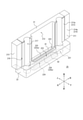
- FIG. 1 is an external perspective view showing an optical connector module 1 including an optical connector 20 according to an embodiment in a top view. An outline of the configuration and function of the optical connector module 1 will be described with reference to FIG. 1.
- the optical connector module 1 is bonded to adjust the refractive index of the optical transmission path 10, the optical connector 20 optically coupled to the optical transmission path 10, and the first space S1 between the optical transmission path 10 and the optical connector 20. It has an agent 30 and.
- the optical connector module 1 has an agent A, which will be described later, for attaching the optical connector 20 to the optical transmission line 10.
- the optical connector 20 is attached to the optical transmission line 10 based on a mounting method including a plurality of steps.
- the mounting method includes, for example, a first step of positioning the optical connector 20 in a state of being mounted on the optical transmission line 10.
- an agent is applied between the optical connector 20 and the optical transmission line 10 from both the left and right sides of the optical connector 20 positioned in the first step.
- the second step is a step for fixing the optical connector 20 to the optical transmission line 10 by using such an agent.
- the "agent” includes, for example, any filler having an adhesive function.
- the agent comprises an adhesive.
- the mounting method is, for example, as shown by an arrow along the upward direction in FIG. 1, from below the optical connector 20 fixed to the optical transmission line 10 in the second step, between the optical transmission line 10 and the optical connector 20.
- the third step of pouring the adhesive 30 into the first space S1 formed in the above is included.
- the adhesive 30 has an adhesive function for fixing the optical connector 20 to the optical transmission path 10 and a function for adjusting the refractive index in the first space S1.
- the third step is a step for fixing the optical connector 20 to the optical transmission line 10 by using such an adhesive 30.
- the optical connector module 1 is optically coupled to another optical transmission line such as an optical fiber and an optical waveguide.
- the optical connector 20 attached to the optical transmission path 10 is connected to a ferrule holding an optical fiber to form an optical coupling between the optical transmission path 10 and the optical fiber.
- the optical connector module 1 can be connected to the optical transmission path 10 by connecting the optical connector 20 attached to the optical transmission path 10 to another optical connector also attached to the optical waveguide. Allows optical coupling with optical waveguides.
- FIG. 2 is an enlarged external perspective view of the optical transmission line 10 of FIG. 1 as an enlarged view.
- the configuration of the optical transmission line 10 will be mainly described with reference to FIG. 2.
- the optical transmission line 10 has a substrate 11 and an optical waveguide 12 laminated on the substrate 11.
- the optical transmission line 10 includes, for example, a substrate 11 composed of a rigid type printed wiring board, and an optical waveguide portion 12 laminated on the upper surface of the substrate 11.
- the optical waveguide 12 is formed in a convex shape so as to project upward from the upper surface of the substrate 11, for example.
- the optical waveguide 12 is formed so that the end face coincides with the end face of the substrate 11 for optical coupling with, for example, the optical connector 20.
- the end face of the optical waveguide 12 is formed in a plane along the end face of the substrate 11, for example.
- the waveguide mode of the optical waveguide unit 12 may be either a single mode or a multi-mode.
- the optical waveguide 12 has a core 121 and a clad 122 laminated on the substrate 11 in a stacking direction orthogonal to the substrate 11. More specifically, the optical waveguide portion 12 is laminated with the first clad 122a laminated on the upper surface of the substrate 11, the core 121 laminated on the first clad 122a, and the core 121 together with the first clad 122a. It has a second clad 122b that is sandwiched in the direction and surrounds the core 121.
- a plurality of cores 121 are formed so as to be separated from each other at predetermined intervals in the left-right direction. Each core 121 extends in the anteroposterior direction.
- the core 121 and the clad 122 are formed of an appropriate material such as quartz-based glass.
- the refractive index of the core 121 is higher than that of the clad 122.
- the optical waveguide portion 12 will be described as, for example, an embedded optical waveguide, but the present invention is not limited thereto.
- the optical waveguide portion 12 may be an optical waveguide of an appropriate type such as a slab type or a semi-embedded type.
- the optical transmission line 10 is manufactured using, for example, photolithography.
- the manufacturing method is carried out in the order of the first clad 122a, the core 121, and the second clad 122b.
- the method for manufacturing the optical transmission line 10 includes a step of laminating the first clad 122a constituting the optical waveguide portion 12 on the substrate 11 in a laminating direction orthogonal to the substrate 11. Subsequently, the method for manufacturing the optical transmission line 10 includes a step of laminating the core 121 constituting the optical waveguide portion 12 on the first clad 122a.
- the method for manufacturing the optical transmission line 10 includes a step of laminating the second clad 122b constituting the optical waveguide portion 12 together with the first clad 122a so as to sandwich the core 121 in the laminating direction.
- FIG. 3 is an external perspective view showing a single optical connector 20 of FIG. An example of the configuration of the optical connector 20 of FIG. 1 will be mainly described with reference to FIG.
- the optical connector 20 is formed in an L shape, for example, by a translucent resin material.
- the optical connector 20 is made of a material having a refractive index close to that of the core 121 of the optical waveguide section 12.
- the optical connector 20 has a first base portion 21 extending in the front-rear direction.
- the optical connector 20 has a recess 212 that is recessed one step upward from the central portion of the lower surface 211 in the left-right direction of the first base portion 21 to the upward direction, that is, inward in the first base portion 21.
- the optical connector 20 has a contact portion 213 that protrudes one step outward in the vertical direction from the lower surface 211 of the first base portion 21.
- the contact portion 213 is located on both the left and right sides with respect to the recess 212.
- the contact portion 213 includes a contact surface 213a located at the lowermost portion of the first base portion 21 in the downward direction, that is, at the tip of the first base portion 21.
- the contact surface 213a is formed at the position most protruding toward the optical transmission path 10 in the first base portion 21.
- the contact surface 213a constitutes the lower tip surface of the first base portion 21.
- the contact portion 213 and the contact surface 213a extend in the front-rear direction over substantially the entire first base portion 21.
- the optical connector 20 has a first adhesive portion 214 formed in a region different from the contact portion 213 in the first base portion 21.
- the first adhesive portion 214 includes a part of the lower surface 211 in the first base portion 21.
- the first adhesive portion 214 is located on the left and right sides of the recess 212 on the outside in the left-right direction with respect to the contact portion 213.
- the first adhesive portion 214 includes an adhesive surface 214a located one step upward, that is, one step inward with respect to the contact surface 213a in the first base portion 21.
- the adhesive surface 214a is located on the side opposite to the optical transmission path 10 with respect to the contact surface 213a in the first base portion 21.
- the adhesive surface 214a has a larger area than the contact surface 213a.
- the first adhesive portion 214 and the adhesive surface 214a extend in the front-rear direction over the entire first base portion 21.
- the optical connector 20 has a side wall 215 that constitutes a side end portion of the first base portion 21.
- the side wall 215 is located on both the left and right sides with respect to the recess 212.
- the first adhesive portion 214 is formed on the side wall 215.
- the adhesive surface 214a of the first adhesive portion 214 constitutes a lower surface of the side wall 215, that is, a part of the lower surface 211.
- the side wall 215 projects on both sides in the left-right direction with respect to the second base portion 22, which will be described later.
- the side wall 215 extends in the front-rear direction over the entire first base 21 at the side end of the first base 21.
- the optical connector 20 has a relief recess 216 formed in the first base portion 21 so as to separate the contact portion 213 and the first adhesive portion 214.
- the relief recess 216 is formed in a groove shape, for example, as a relief groove.
- the relief recess 216 is sandwiched between the contact portion 213 and the first adhesive portion 214, and is located on both the left and right sides of the recess 212.
- the relief recess 216 extends in the front-rear direction over the entire first base 21.
- the optical connector 20 has a positioning portion 217 recessed in the first base portion 21 so as to sandwich the contact portion 213 together with the side wall 215. From another viewpoint, the positioning portion 217 is recessed in the central portion of the contact portion 213. The positioning portion 217 is located on both the left and right sides with respect to the recess 212. The positioning portion 217 extends in the front-rear direction over the entire first base portion 21. The positioning portion 217 is formed continuously from the through hole 221 of the second base portion 22, which will be described later, to the rear end of the first base portion 21. The positioning portion 217 is a concave portion formed in a semicircular shape in a cross-sectional view. The through hole 221 and the positioning portion 217 are formed concentrically with each other.
- the optical connector 20 is formed in an L shape and has a second base portion 22 protruding from the first base portion 21 in a direction orthogonal to the extending direction of the first base portion 21.
- the second base portion 22 projects forward of the first base portion 21 and is formed so as to be continuous with the first base portion 21.
- the second base portion 22 is formed so as to project downward from the first base portion 21.
- the optical connector 20 has a circular through hole 221 in a cross-sectional view that penetrates from the front surface to the rear surface of the second base portion 22.
- Through holes 221 are formed at both left and right ends of the second base portion 22 so as to correspond to the positioning portion 217 of the first base portion 21 and to be located on both the left and right sides of the recess 212 of the first base portion 21.
- the optical connector 20 has a first notched portion 222 in which the inner surface of the second base portion 22 is cut out to the first side surface A1.
- the first notch 222 is formed as a concave shape.
- the optical connector 20 has a second surface composed of four side surfaces, top, bottom, left, and right, constituting the first notch 222, a first side surface A1, and an inner surface of a second base 22 located directly below the first notch 222. It has an adhesive portion 223.
- the optical connector 20 has a second cutout portion 224 in which the outer surface of the second base portion 22 is cut out to the second side surface A2.
- the second notch 224 is formed in a concave shape.
- the optical connector 20 has a first lens portion 225 provided on the first side surface A1 forming a part of the first notch portion 222.
- the first lens unit 225 is composed of a plurality of curved lenses 225a.
- the number of lenses 225a constituting the first lens unit 225 corresponds to the number of cores 121 of the optical transmission line 10.
- the optical connector 20 constitutes a part of the second notch portion 224, and has a second lens portion 226 provided on the second side surface A2 located on the side opposite to the first side surface A1 in the light propagation direction.
- the second lens unit 226 is composed of a plurality of curved lenses 226a.
- the number of lenses 226a constituting the second lens unit 226 corresponds to the number of cores 121 of the optical transmission line 10.
- FIG. 4 is a cross-sectional view taken along the IV-IV arrow line of FIG.
- FIG. 5 is an enlarged view of the broken line box V in FIG. 4.
- FIG. 6 is an enlarged view of the dashed line box VI of FIG. 5 which is further enlarged.
- the optical connector 20 is mounted on the optical waveguide 12 from above the optical transmission line 10.
- the optical connector 20 is arranged in a state where the first base portion 21 is in contact with the upper surface of the optical waveguide portion 12 and partially covers a part of the optical transmission path 10.
- the second base portion 22 is arranged so as to project forward from the end portion of the substrate 11 and project downward from the first base portion 21.
- the second base portion 22 projects downward so that its lower surface is located further below the vertical position of the optical waveguide portion 12.
- the second base 22 faces the surface of the optical transmission line 10, that is, the end surface of the optical transmission line 10 orthogonal to the upper surface.
- the first space S1 is formed between the optical transmission line 10 and the optical connector 20.
- the inner surface of the second base 22 on which the first notch 222 of the optical connector 20 is formed is separated from the end surface of the substrate 11.
- the adhesive 30 is filled from below so as to fill the first space S1.
- the adhesive 30 is made of a material having a refractive index close to that of the core 121 of the optical transmission line 10.
- the adhesive 30 is interposed between the end surface of the optical transmission path 10 and the first side surface A1 to adjust the refractive index on the optical path between the core 121 and the first side surface A1.
- the second adhesive portion 223 of the optical connector 20 and the adhesive 30 adhere to each other.
- the end face of the optical transmission line 10 and the adhesive 30 adhere to each other.
- the adhesive 30 is in close contact with the end faces of the second adhesive portion 223 and the optical transmission path 10 in a state of being filled inside the first lens portion 225 and the first notch portion 222. As described above, the optical connector 20 is fixed to the optical transmission line 10 by the adhesive 30.
- the optical connector 20 is optically coupled to the optical waveguide 12 included in the optical transmission line 10 in a state of being fixed to the optical transmission line 10.
- the first side surface A1 faces the end surface of the core 121.
- the first lens unit 225 faces the end surface of the core 121.
- the adhesive 30 is interposed between the first lens portion 225 and the end face of the core 121.
- the lens 225a constituting the first lens portion 225 is formed as a concave shape on the first side surface A1.
- the lens 225a is formed as a concave lens.
- the lens 225a is formed in an arc shape in a cross-sectional view as shown in FIG. 6 along the light propagation direction, that is, the front-back direction.
- the vertical half width (radius) of the lens 225a is larger than the radius of the core 121 of the optical transmission line 10.
- the second lens portion 226 faces the first lens portion 225 via the second base portion 22 of the optical connector 20.
- the lens 226a constituting the second lens portion 226 is formed as a convex shape on the second side surface A2.
- the lens 226a is formed as a convex lens.
- the lens 226a is formed in an arc shape in a cross-sectional view as shown in FIG. 5 along the light propagation direction, that is, the front-rear direction.
- the vertical half width (radius) of the lens 226a is larger than the radius of the core 121 of the optical transmission line 10.
- the optical transmission line 10 will be described as transmitting light from a light emitting element. Not limited to this, the optical transmission path 10 may transmit light to the light receiving element. In this case, it should be understood that the following explanation applies with the light propagation direction reversed.
- the adhesive 30 is composed of a material having a refractive index close to the refractive index of the core 121, the Frenel reflection of light incident on the interface between the adhesive 30 and the core 121 is suppressed by the matching of the refractive indexes. .. Therefore, the light incident on the boundary surface is emitted to the inside of the adhesive 30 with high transmittance.
- the light emitted from the core 121 is incident on the lens 225a while spreading due to the diffraction effect inside the adhesive 30.
- the optical connector 20 is made of a material having a refractive index close to the refractive index of the adhesive 30, the Fresnel reflection of light incident on the interface between the optical connector 20 and the adhesive 30 is due to the matching of the refractive indexes. It is suppressed. Therefore, the light incident on the boundary surface is emitted to the inside of the optical connector 20, for example, the second base portion 22 with high transmittance.
- the lens 225a When the lens 225a is formed as a concave lens, the light emitted into the inside of the second base 22 is incident on the lens 226a while further spreading.
- the lens 226a When the lens 226a is formed as a convex lens, the light incident on the boundary surface between the outside and the optical connector 20 is collimated by, for example, the lens 226a. In this way, the optical connector module 1 propagates, for example, the light emitted from the optical transmission line 10 to the outside in a collimated state.
- the light emitted from the optical connector module 1 is coupled to another optical transmission line.
- the light is coupled to an optical fiber held by a ferrule connected to the optical connector 20.
- light is coupled to an optical waveguide to which another optical connector connected to the optical connector 20 is attached.
- FIG. 6 shows the state of the end face of the optical transmission line 10 of FIG.
- the end face of the optical waveguide portion 12 coincides with the end face of the substrate 11.
- the end faces of the core 121 and the clad 122 are formed in the same plane along the end faces of the substrate 11.
- the present invention is not limited to this, and the end face of the optical waveguide 12, for example, the end face of the core 121 may be a curved surface protruding toward the optical connector 20.
- the end face of the core 121 may be a curved surface that protrudes toward the optical connector 20 from the end face of the clad 122.
- FIG. 7 is a diagram schematically showing a cross section of the optical connector module 1 of FIG. 1 from the front. With reference to FIG. 7, the configuration and function of the optical connector 20 related to the optical transmission line 10 will be mainly described.
- the first base 21 is mounted on the optical transmission line 10.
- the contact portion 213 formed on the first base portion 21 comes into contact with the mounting surface of the optical transmission path 10.
- the contact surface 213a formed as the tip surface of the first base portion 21 abuts on the upper surface of the first clad 122a of the optical waveguide portion 12.
- the vertical position of the optical connector 20 with respect to the optical transmission path 10 is determined based on the contact between the contact surface 213a of the first base portion 21 and the upper surface of the first clad 122a of the optical waveguide portion 12. ..
- the optical connector 20 may be positioned in the front-back and left-right directions with respect to the optical transmission line 10 by an appropriate method.
- the optical connector 20 may be positioned in the front-rear and left-right directions by engaging the positioning portion 217 with the stud pin formed on the first clad 122a.
- the first adhesive portion 214 is separated from the surface of the optical transmission path 10.
- the adhesive surface 214a located one step inside the contact surface 213a in the first base portion 21 is separated from the upper surface of the first clad 122a of the optical waveguide portion 12.
- a second space S2 in which the agent A for attaching the optical connector 20 to the optical transmission line 10 is interposed is formed between the first adhesive portion 214 and the surface of the optical transmission line 10.
- the second space S2 is surrounded by the surface of the optical transmission line 10, the adhesive surface 214a, and the contact portion 213. More specifically, the second space S2 is surrounded by the upper surface of the first clad 122a, the adhesive surface 214a, and the outer wall in the left-right direction at the contact portion 213.
- the agent A is filled from the left and right sides of the optical connector 20 into the second space S2 formed between the optical connector 20 and the optical transmission path 10. At this time, the agent A forms a fillet F in the vicinity of the corner C of the side wall 215 of the optical connector 20. Even if the amount of the agent A is excessive, the surplus amount of the agent A is stored in the escape recess 216.
- the optical connector 20 is fixed to the optical transmission line 10 by the agent A.
- the adhesive surface 214a of the optical connector 20 and the agent A adhere to each other.
- the upper surface of the first clad 122a of the optical transmission line 10 and the agent A adhere to each other.
- the optical connector 20 since the optical transmission path 10 and the optical connector 20 are securely fixed, it is desired to suppress the positional deviation of the optical connector 20 with respect to the optical transmission path 10. Makes it possible to maintain optical characteristics. For example, by forming the second space S2 in which the agent A is interposed between the first adhesive portion 214 and the surface of the optical transmission path 10, the optical connector 20 is subjected to optical transmission in the second step of the mounting method. It can be fixed to the road 10. At this time, the optical connector 20 can be fixed to the optical transmission line 10 by the agent A while maintaining the contact between the contact surface 213a of the optical connector 20 and the mounting surface of the optical transmission line 10. Is.
- the agent A does not flow toward the recess 212a with respect to the contact surface 213a in contact with the first clad 122a. Therefore, the highly accurate positioning function can be maintained without the agent A flowing into the positioning portion 217.
- the abutting portions 213 are located at both left and right ends with respect to the recess 212, so that in the second step of fixing to the optical transmission path 10 using the agent A, the abutting portion 213 is in the vertical direction of the optical connector 20 with respect to the optical transmission path 10. Stabilize positioning.
- the contact portion 213 suppresses the flow of the agent A into the positioning portion 217, and also suppresses the adhesive 30 from flowing into the positioning portion 217 in the third step of pouring the adhesive 30. Therefore, the positioning of the optical connector 20 with respect to the optical transmission path 10 is performed more stably.
- the contact surface 213a and the optical transmission path 10 are mounted.
- the contact with the mounting surface is reliably maintained.
- the intrusion of the adhesive 30 into the contact portion between the contact surface 213a and the mounting surface of the optical transmission path 10 is suppressed.
- the possibility that the adhesive 30 will flow between the optical connector 20 and the optical transmission line 10 in a place where the adhesive 30 does not flow in the original design is reduced.
- the positional deviation of the optical connector 20 with respect to the optical transmission path 10 is suppressed, and the optical connector 20 is reliably maintained at the original design position.
- the optical connector 20 attached to the optical transmission line 10 can maintain the desired optical characteristics.
- the contact portion 213 facilitates the vertical positioning of the optical connector 20 with respect to the optical transmission path 10. Become stable.
- the contact surface 213a can come into contact with the smoothest surface in the optical transmission line 10 by abutting on the upper surface of the first clad 122a. This improves the vertical positioning accuracy of the optical connector 20 with respect to the optical transmission line 10.
- the surface of the optical transmission path 10 is processed by the first adhesive portion 214 including the adhesive surface 214a located on the opposite side of the contact surface 213a with respect to the contact surface 213a in the first base portion 21.
- the second space S2 can be formed without any problem. For example, since a step is formed along the vertical direction between the contact surface 213a and the adhesive surface 214a, the agent A is interposed between the first adhesive portion 214 and the surface of the optical transmission path 10. The second space S2 can be easily formed.
- the adhesive surface 214a, and the contact portion 213, By surrounding the second space S2 with the surface of the optical transmission path 10, the adhesive surface 214a, and the contact portion 213, it becomes easy to fill the second space S2 with the agent A. As a result, the adhesive surface 214a of the optical connector 20 and the agent A are surely adhered to each other. Similarly, the surface of the optical transmission line 10 and the agent A are surely adhered to each other. As a result, the optical connector 20 can be reliably fixed to the optical transmission line 10.
- the area of the adhesive surface 214a is larger than the area of the contact surface 213a, the fixing strength of the optical connector 20 to the optical transmission line 10 is increased. Therefore, the invasion of the adhesive 30 into the contact portion between the contact surface 213a and the mounting surface of the optical transmission path 10 is more effectively suppressed. As a result, the misalignment of the optical connector 20 with respect to the optical transmission path 10 is more effectively suppressed, and the optical connector 20 is reliably maintained at the original design position. As a result, the optical connector 20 attached to the optical transmission line 10 can more easily maintain the desired optical characteristics.
- the first adhesive portion 214 is formed on the side wall 215 constituting the side end portion of the first base portion 21, it is easy to interpose the agent A in the second space S2 in the second step of the mounting method. become.
- the fixing of the optical connector 20 to the optical transmission line 10 can be easily achieved by a simple operation of applying the agent A from the outside of the side wall 215. Therefore, the positional deviation of the optical connector 20 with respect to the optical transmission path 10 is easily suppressed, and the desired optical characteristics can be easily maintained.
- the optical connector 20 can be positioned in the front-back and left-right directions with respect to the optical transmission path 10.
- the positioning unit 217 enables positioning in the front-back and left-right directions, so that light with respect to the optical transmission path 10 can be obtained.
- the positioning accuracy of the connector 20 is improved.
- the optical connector 20 By projecting the side wall 215 to both sides in the left-right direction with respect to the second base portion 22, for example, when injection molding is performed, the optical connector 20 is separated from the contact portion 213, which requires high accuracy in design. It is possible to poke the ejector pin against. In this way, the optical connector 20 is pierced by the ejector pin at a position separated from the contact portion 213. Therefore, defects such as burrs and warpage of the contact portion 213 are suppressed.
- a manufacturing machine or the like uses an arm or the like to provide a side wall of the optical connector 20.
- the 215 can be easily held.
- the side wall 215, which is a holding portion by the arm or the like, and the contact portion 213 are separated from each other, the possibility that the arm or the like comes into contact with the contact portion 213, which requires high accuracy in design, is reduced. Therefore, defects such as deformation of the contact portion 213 due to such contact are suppressed.
- the optical connector module 1 can reduce the bonding loss by interposing the adhesive 30.
- the optical connector module 1 can reduce a loss due to a diffraction effect, a loss due to scattering or absorption of light due to a foreign substance from the outside, a loss due to Fresnel reflection, and the like.
- the adhesive 30 having a refractive index close to the refractive index of the core 121 is arranged in the optical path, so that the light spreads due to the diffraction effect as compared with the case in the air. Can be suppressed.
- the optical connector module 1 can reduce the proportion of light that does not combine with the first lens unit 225 due to the diffraction effect.
- the adhesive 30 also plays a role of suppressing the mixing of foreign substances.
- the first space S1 is filled with the adhesive 30, so that foreign matter can be suppressed from being mixed in from the outside.
- the optical connector module 1 can suppress the loss due to scattering or absorption of light due to foreign matter from the outside, and can reduce the coupling loss.
- the optical connector module 1 can emit light from the core 121 with high transmittance and improve the coupling efficiency.
- the optical connector module 1 has a second lens portion 226 having a curvature, which enables optical adjustment by two lens portions combined with the first lens portion 225.
- the optical connector module 1 can improve the degree of freedom of optical adjustment by the two lens portions. Thereby, the optical connector module 1 can easily provide the emitted light having a desired beam state.
- the first lens portion 225 is formed as a concave lens, so that the light emitted from the core 121 can be forcibly expanded.
- the optical connector module 1 is provided with a concave lens at a position facing the core 121 on the first side surface A1, so that the light whose spread is suppressed by the adhesive 30 can be forcibly spread at an early stage after emission.
- the second lens portion 226 is formed as a convex lens in the optical connector module 1, the light spread by the first lens portion 225 of the concave lens can be converted into collimated light.
- the optical connector module 1 can provide collimated light having a large aperture by combining a concave lens and a convex lens by the first lens unit 225 and the second lens unit 226. As a result, the optical connector module 1 can provide collimated light that can be efficiently focused on a smaller spot.
- the optical connector module 1 can irradiate collimated light having good characteristics.
- the optical connector module 1 can expand the allowable range of optical coupling by collimated light with a large diameter. In other words, the optical connector module 1 enables optical coupling within a predetermined allowable range even if the optical axis is deviated from another optical transmission line to be optical coupled.
- the optical transmission line 10 and the optical connector 20 are fixed by the adhesive 30, so that the optical axis shift due to use and deterioration over time can be suppressed. Therefore, the optical connector module 1 can maintain the same optical characteristics for a long period of time in a state where the relative positions with respect to each other are determined by the initial positioning. In this way, the optical connector module 1 can improve the quality as a product.
- the optical connector module 1 is made of a material having a refractive index close to the refractive index of the core 121 together with the adhesive 30, the optical connector 20 can suppress Frenel reflection and reduce the coupling loss.
- the shape, arrangement, orientation, and number of each component described above are not limited to the contents shown in the above description and drawings.
- the shape, arrangement, orientation, and number of each component may be arbitrarily configured as long as the function can be realized.
- the contact portion 213 includes the contact surface 213a, but the present invention is not limited to this.
- the contact portion 213 may include one or more protrusions or the like instead of the contact surface 213a.
- the vertical positioning of the optical connector 20 with respect to the optical transmission path 10 may be performed by abutting between such a protrusion and the mounting surface of the optical transmission path 10.
- FIG. 8 is a diagram corresponding to FIG. 7, which schematically shows a modified example of the optical connector module 1 of FIG.
- the adhesive surface 214a is located one step inside the contact surface 213a in the first base portion 21, and the first adhesive portion 214 and the contact portion 213 are separated by a step.
- the adhesive surface 214a of the first adhesive portion 214 may be located on the same surface as the contact surface 213a in the first base portion 21.
- a second space S2 in which the agent A is interposed is formed between the first adhesive portion 214 and the surface of the optical transmission path 10. good.
- the second space S2 may be surrounded by the upper surface of the substrate 11 of the optical transmission path 10, the adhesive surface 214a, and the first clad 122a.
- the relief recess 216 separates the contact surface 213a and the adhesive surface 214a at the first base portion 21.
- the division between the first adhesive portion 214 and the contact portion 213 may be achieved by the relief recess 216 instead of the step.
- the contact surface 213a and the adhesive surface 214a are formed on the same surface, so that the shape of the optical connector 20 can be simplified. Even if the optical connector 20 has such a simple shape, it is possible to form the second space S2, and the above-mentioned matters relating to the suppression of the positional deviation of the optical connector 20 with respect to the optical transmission path 10 and the maintenance of desired optical characteristics. The same effect applies.
- the relief recess 216 separates the contact surface 213a and the adhesive surface 214a, so that even if the amount of the agent A is excessive, the surplus amount of the agent A is stored in the escape recess 216.
- the intrusion of the agent A into the contact portion between the contact surface 213a and the mounting surface of the optical transmission path 10 is suppressed. Therefore, the displacement of the optical connector 20 with respect to the optical transmission path 10 is suppressed, and the optical connector 20 is reliably maintained at the original design position. As a result, the optical connector 20 attached to the optical transmission line 10 can maintain the desired optical characteristics.
- the optical connector 20 has a relief recess 216, but the present invention is not limited to this. If the agent A used for fixing the optical connector 20 to the optical transmission line 10 can be maintained in an appropriate amount, the relief recess 216 is not formed in both the optical connector 20 shown in FIGS. 7 and 8. You may.
- the area of the adhesive surface 214a is larger than the area of the contact surface 213a, but the present invention is not limited to this.
- the area of the adhesive surface 214a may be less than or equal to the area of the contact surface 213a as long as the strength required for fixing the optical connector 20 to the optical transmission path 10 is maintained.
- the first adhesive portion 214 is formed on the side wall 215, but the present invention is not limited to this.
- the first adhesive portion 214 may be formed at any position in the optical connector 20 as long as the required function can be realized.
- the optical connector 20 has a positioning portion 217 recessed in the first base portion 21, but the present invention is not limited to this.
- the optical connector 20 may have a convex portion that fits into a concave portion formed on the optical transmission path 10. At this time, the optical connector 20 may be positioned in the front-back, left-right, up-down directions by fitting the convex portion into the concave portion.
- the optical connector 20 is positioned with respect to the optical transmission line 10 by the positioning unit 217, but the present invention is not limited to this.
- the optical connector 20 may be positioned by abutting at least one of the inner side surfaces of the recess 212 along the front-rear direction with the left-right end surface of the optical waveguide portion 12 protruding from the substrate 11.
- the side wall 215 of the optical connector 20 is continuously formed in a flat plate shape, but the present invention is not limited to this.
- the side wall 215 may not be continuous, and may be formed in a state of being divided by an arbitrary number, shape, height, and arrangement by one or more slits.
- the adhesive area between the agent A and the first adhesive portion 214 is increased, so that the fixing strength of the optical connector 20 with respect to the optical transmission path 10 is improved.
- the adhesive surface 214a constituting the lower surface of the side wall 215 is a flat surface, but the present invention is not limited to this.
- the adhesive surface 214a may be composed of a surface having an arbitrary shape including a curved surface, an inclined surface, and the like.
- recesses or through holes may be formed on the adhesive surface 214a in any number, shape, height, and arrangement toward the opposite side of the optical transmission path 10. By forming such a recess or a through hole on the adhesive surface 214a, even if the amount of the agent A is excessive, the surplus amount of the agent A can be accommodated in the recess or the through hole.
- the shape of the bonding surface 214a and the number, shape, height, arrangement, etc. of the recesses or through holes are appropriately determined. May be good.
- the angle C of the side wall 215 of the optical connector 20 is a right angle, but the present invention is not limited to this.
- a surface having an arbitrary shape such as a C surface and an R surface may be formed at the angle C of the side wall 215.
- the optical waveguide portion 12 is formed on the upper surface of the substrate 11, but the present invention is not limited to this.
- the optical waveguide 12 may be embedded inside the substrate 11.
- the end face of the optical waveguide portion 12 may be formed so as to coincide with the end face of the substrate 11 and the end face of the core 121 to be exposed from the substrate 11.
- the adhesive 30 fills only the first space S1, but the present invention is not limited to this.
- the adhesive 30 may be filled in addition to the first space S1 so as to fill the recess 212 of the optical connector 20 that covers the optical transmission path 10.
- the contact portion 213 and the contact surface 213a extend in the front-rear direction over substantially the entire first base portion 21, but the present invention is not limited to this.
- the contact portion 213 and the contact surface 213a may be formed by any shape, arrangement, orientation, and number capable of realizing the function.
- the contact portion 213 and the contact surface 213a may extend in the front-rear direction over a part of the first base portion 21.
- the same description applies to the first adhesive portion 214, the side wall 215, the relief recess 216, and the positioning portion 217.
- the contact surface 213a abuts on the upper surface of the first clad 122a, but the present invention is not limited to this.
- the contact surface 213a may abut on any surface of the optical transmission line 10.
- the contact surface 213a may abut on the upper surface of the substrate 11 or may abut on the upper surface of the second clad 122b.
- the shapes of the first lens portion 225 and the second lens portion 226 have been described as being arcuate in cross-sectional view, but the shape is not limited to this.
- the shapes of the first lens portion 225 and the second lens portion 226 may be spherical or aspherical.
- the first lens unit 225 has been described as a concave lens, but the present invention is not limited to this.
- the first lens unit 225 may be any type of lens such as a convex lens as long as the desired optical characteristics can be obtained.
- the optical connector 20 does not have to have the second lens portion 226 as long as the desired optical characteristics can be obtained.
- the second lens unit 226 is not limited to a convex lens, and may be any type of lens such as a concave lens.
- Optical connector module 10 Optical transmission line 11
- Base 12 Optical waveguide 121 Core 122 Clad 122a 1st clad 122b 2nd clad 20
- Optical connector 21 1st base 211 Bottom surface 212 Recess 213 Contact 213a Contact surface 214 1st adhesive (Adhesive part) 214a Adhesive surface 215 Side wall 216 Relief recess 217 Positioning part 22 Second base part 221 Through hole 222 First notch part 223 Second adhesive part 224 Second notch part 225 First lens part 225a Lens 226 Second lens part 226a Lens 30
Landscapes
- Physics & Mathematics (AREA)
- General Physics & Mathematics (AREA)
- Optics & Photonics (AREA)
- Optical Couplings Of Light Guides (AREA)
- Mechanical Coupling Of Light Guides (AREA)
Abstract
La présente invention concerne un connecteur optique (20) qui est fixé à un trajet de transmission optique (10) comprenant un substrat (11) et une partie de guide d'ondes optique (12) empilée sur le substrat (11), le connecteur optique (20) étant pourvu d'une première partie de base (21) qui est montée sur le trajet de transmission optique (10), d'une partie de butée (213) qui est formée dans la première partie de base (21) et qui vient en butée sur une surface de montage du trajet de transmission optique (10), et d'une partie de liaison (214) qui est formée dans une région différente de la partie de butée (213) dans la première partie de base (21) et qui est séparée de la surface du trajet de transmission optique (10) ; entre la partie de liaison (214) et la surface du trajet de transmission optique (10), il est formé un espace (S2) dans lequel est présent un matériau (A) pour fixer le connecteur optique (20) au trajet de transmission optique (10).
Priority Applications (3)
| Application Number | Priority Date | Filing Date | Title |
|---|---|---|---|
| EP21841441.5A EP4184227A4 (fr) | 2020-07-17 | 2021-07-06 | Connecteur optique et module de connecteur optique |
| US18/016,214 US12487414B2 (en) | 2020-07-17 | 2021-07-06 | Optical connector and optical connector module |
| CN202180060942.7A CN116157714B (zh) | 2020-07-17 | 2021-07-06 | 光连接器以及光连接器模块 |
Applications Claiming Priority (2)
| Application Number | Priority Date | Filing Date | Title |
|---|---|---|---|
| JP2020-123188 | 2020-07-17 | ||
| JP2020123188A JP7566519B2 (ja) | 2020-07-17 | 2020-07-17 | 光コネクタ及び光コネクタモジュール |
Publications (1)
| Publication Number | Publication Date |
|---|---|
| WO2022014419A1 true WO2022014419A1 (fr) | 2022-01-20 |
Family
ID=79554765
Family Applications (1)
| Application Number | Title | Priority Date | Filing Date |
|---|---|---|---|
| PCT/JP2021/025518 Ceased WO2022014419A1 (fr) | 2020-07-17 | 2021-07-06 | Connecteur optique et module de connecteur optique |
Country Status (5)
| Country | Link |
|---|---|
| US (1) | US12487414B2 (fr) |
| EP (1) | EP4184227A4 (fr) |
| JP (1) | JP7566519B2 (fr) |
| CN (1) | CN116157714B (fr) |
| WO (1) | WO2022014419A1 (fr) |
Citations (10)
| Publication number | Priority date | Publication date | Assignee | Title |
|---|---|---|---|---|
| JP2000019343A (ja) * | 1998-07-02 | 2000-01-21 | Nippon Telegr & Teleph Corp <Ntt> | 光導波路素子 |
| JP2007110594A (ja) * | 2005-10-17 | 2007-04-26 | Hitachi Maxell Ltd | カメラモジュール |
| JP2013171112A (ja) * | 2012-02-20 | 2013-09-02 | Sumitomo Electric Ind Ltd | 光モジュール |
| JP2013200550A (ja) * | 2012-02-20 | 2013-10-03 | Sumitomo Electric Ind Ltd | レンズ部品及びそれを備えた光モジュール |
| US20140270626A1 (en) * | 2013-03-14 | 2014-09-18 | Corning Cable Systems Llc | Circuit board(s) employing optical interfaces optically connected to surface-accessible, planar-shaped, inter-board optical fiber traces, and related connectors, assemblies, and methods |
| JP2016009081A (ja) | 2014-06-24 | 2016-01-18 | 富士通コンポーネント株式会社 | 光コネクタの製造方法及び光コネクタ |
| WO2017072993A1 (fr) * | 2015-10-28 | 2017-05-04 | 京セラコネクタプロダクツ株式会社 | Connecteur optique, système de connecteur optique et câble optique actif pourvu de celui-ci |
| JP2017204541A (ja) * | 2016-05-10 | 2017-11-16 | 株式会社リコー | 光源ユニット及びレーザユニット |
| WO2017208285A1 (fr) * | 2016-06-03 | 2017-12-07 | 京セラ株式会社 | Connecteur optique |
| WO2018229992A1 (fr) * | 2017-06-16 | 2018-12-20 | 京セラ株式会社 | Module de connecteur optique |
Family Cites Families (6)
| Publication number | Priority date | Publication date | Assignee | Title |
|---|---|---|---|---|
| JP2552187B2 (ja) * | 1989-10-20 | 1996-11-06 | 日本電信電話株式会社 | 高精度接着方法 |
| JP2699242B2 (ja) * | 1992-05-26 | 1998-01-19 | 株式会社フジクラ | 光ファイバ接続用コネクタ |
| JP4929821B2 (ja) * | 2006-04-27 | 2012-05-09 | オムロン株式会社 | 光伝送モジュール |
| JP2013097064A (ja) * | 2011-10-28 | 2013-05-20 | Kyocera Corp | 光コネクタおよび光コネクタの製造方法 |
| CN107430246B (zh) * | 2015-04-27 | 2019-12-27 | 京瓷株式会社 | 光传输模块 |
| WO2017212861A1 (fr) * | 2016-06-07 | 2017-12-14 | 京セラ株式会社 | Connecteur optique |
-
2020
- 2020-07-17 JP JP2020123188A patent/JP7566519B2/ja active Active
-
2021
- 2021-07-06 US US18/016,214 patent/US12487414B2/en active Active
- 2021-07-06 WO PCT/JP2021/025518 patent/WO2022014419A1/fr not_active Ceased
- 2021-07-06 EP EP21841441.5A patent/EP4184227A4/fr active Pending
- 2021-07-06 CN CN202180060942.7A patent/CN116157714B/zh active Active
Patent Citations (10)
| Publication number | Priority date | Publication date | Assignee | Title |
|---|---|---|---|---|
| JP2000019343A (ja) * | 1998-07-02 | 2000-01-21 | Nippon Telegr & Teleph Corp <Ntt> | 光導波路素子 |
| JP2007110594A (ja) * | 2005-10-17 | 2007-04-26 | Hitachi Maxell Ltd | カメラモジュール |
| JP2013171112A (ja) * | 2012-02-20 | 2013-09-02 | Sumitomo Electric Ind Ltd | 光モジュール |
| JP2013200550A (ja) * | 2012-02-20 | 2013-10-03 | Sumitomo Electric Ind Ltd | レンズ部品及びそれを備えた光モジュール |
| US20140270626A1 (en) * | 2013-03-14 | 2014-09-18 | Corning Cable Systems Llc | Circuit board(s) employing optical interfaces optically connected to surface-accessible, planar-shaped, inter-board optical fiber traces, and related connectors, assemblies, and methods |
| JP2016009081A (ja) | 2014-06-24 | 2016-01-18 | 富士通コンポーネント株式会社 | 光コネクタの製造方法及び光コネクタ |
| WO2017072993A1 (fr) * | 2015-10-28 | 2017-05-04 | 京セラコネクタプロダクツ株式会社 | Connecteur optique, système de connecteur optique et câble optique actif pourvu de celui-ci |
| JP2017204541A (ja) * | 2016-05-10 | 2017-11-16 | 株式会社リコー | 光源ユニット及びレーザユニット |
| WO2017208285A1 (fr) * | 2016-06-03 | 2017-12-07 | 京セラ株式会社 | Connecteur optique |
| WO2018229992A1 (fr) * | 2017-06-16 | 2018-12-20 | 京セラ株式会社 | Module de connecteur optique |
Non-Patent Citations (1)
| Title |
|---|
| See also references of EP4184227A4 |
Also Published As
| Publication number | Publication date |
|---|---|
| EP4184227A4 (fr) | 2024-10-16 |
| US12487414B2 (en) | 2025-12-02 |
| JP7566519B2 (ja) | 2024-10-15 |
| EP4184227A1 (fr) | 2023-05-24 |
| JP2022019384A (ja) | 2022-01-27 |
| US20230280555A1 (en) | 2023-09-07 |
| CN116157714A (zh) | 2023-05-23 |
| CN116157714B (zh) | 2026-03-20 |
Similar Documents
| Publication | Publication Date | Title |
|---|---|---|
| CN110741295B (zh) | 光连接器模块 | |
| JP2005115346A (ja) | 光導波路構造体及び光モジュール | |
| JP6676412B2 (ja) | 光レセプタクル、光モジュールおよび光モジュールの製造方法 | |
| JP6681751B2 (ja) | 光レセプタクルおよび光モジュール | |
| JP6979381B2 (ja) | 光コネクタモジュール | |
| WO2015107923A1 (fr) | Réceptacle de lumière et module d'éclairage | |
| WO2022014419A1 (fr) | Connecteur optique et module de connecteur optique | |
| WO2022024855A1 (fr) | Connecteur optique et module de connecteur optique | |
| WO2017154541A1 (fr) | Réceptacle optique et module optique | |
| JP7493669B2 (ja) | 双方向通信を支援する光コネクタ | |
| JP2017161579A (ja) | 光レセプタクルおよび光モジュール | |
| US20260063855A1 (en) | Optical receptacle and optical module | |
| JP2025058704A (ja) | 光レセプタクルおよび光モジュール | |
| WO2023100899A1 (fr) | Connecteur optique et module de connecteur optique | |
| JP2006091684A (ja) | 光導波路構造体および光モジュール | |
| WO2025154619A1 (fr) | Premier module de connecteur optique et système de connecteur optique | |
| WO2025154620A1 (fr) | Premier module de connecteur optique et système de connecteur optique | |
| JP2005189757A (ja) | 光モジュール | |
| JP2007212902A (ja) | 光送受信装置 | |
| JP2007212901A (ja) | 光通信装置 |
Legal Events
| Date | Code | Title | Description |
|---|---|---|---|
| 121 | Ep: the epo has been informed by wipo that ep was designated in this application |
Ref document number: 21841441 Country of ref document: EP Kind code of ref document: A1 |
|
| NENP | Non-entry into the national phase |
Ref country code: DE |
|
| ENP | Entry into the national phase |
Ref document number: 2021841441 Country of ref document: EP Effective date: 20230217 |
|
| WWW | Wipo information: withdrawn in national office |
Ref document number: 2021841441 Country of ref document: EP |