WO2022071283A1 - Élément de guide d'ondes optique, et dispositif de modulation optique et dispositif de transmission optique qui l'utilisent - Google Patents
Élément de guide d'ondes optique, et dispositif de modulation optique et dispositif de transmission optique qui l'utilisent Download PDFInfo
- Publication number
- WO2022071283A1 WO2022071283A1 PCT/JP2021/035550 JP2021035550W WO2022071283A1 WO 2022071283 A1 WO2022071283 A1 WO 2022071283A1 JP 2021035550 W JP2021035550 W JP 2021035550W WO 2022071283 A1 WO2022071283 A1 WO 2022071283A1
- Authority
- WO
- WIPO (PCT)
- Prior art keywords
- optical waveguide
- optical
- substrate
- modulation
- waveguide element
- Prior art date
- Legal status (The legal status is an assumption and is not a legal conclusion. Google has not performed a legal analysis and makes no representation as to the accuracy of the status listed.)
- Ceased
Links
Images








Classifications
-
- G—PHYSICS
- G02—OPTICS
- G02F—OPTICAL DEVICES OR ARRANGEMENTS FOR THE CONTROL OF LIGHT BY MODIFICATION OF THE OPTICAL PROPERTIES OF THE MEDIA OF THE ELEMENTS INVOLVED THEREIN; NON-LINEAR OPTICS; FREQUENCY-CHANGING OF LIGHT; OPTICAL LOGIC ELEMENTS; OPTICAL ANALOGUE/DIGITAL CONVERTERS
- G02F1/00—Devices or arrangements for the control of the intensity, colour, phase, polarisation or direction of light arriving from an independent light source, e.g. switching, gating or modulating; Non-linear optics
- G02F1/01—Devices or arrangements for the control of the intensity, colour, phase, polarisation or direction of light arriving from an independent light source, e.g. switching, gating or modulating; Non-linear optics for the control of the intensity, phase, polarisation or colour
- G02F1/03—Devices or arrangements for the control of the intensity, colour, phase, polarisation or direction of light arriving from an independent light source, e.g. switching, gating or modulating; Non-linear optics for the control of the intensity, phase, polarisation or colour based on ceramics or electro-optical crystals, e.g. exhibiting Pockels effect or Kerr effect
- G02F1/035—Devices or arrangements for the control of the intensity, colour, phase, polarisation or direction of light arriving from an independent light source, e.g. switching, gating or modulating; Non-linear optics for the control of the intensity, phase, polarisation or colour based on ceramics or electro-optical crystals, e.g. exhibiting Pockels effect or Kerr effect in an optical waveguide structure
-
- G—PHYSICS
- G02—OPTICS
- G02B—OPTICAL ELEMENTS, SYSTEMS OR APPARATUS
- G02B6/00—Light guides; Structural details of arrangements comprising light guides and other optical elements, e.g. couplings
- G02B6/10—Light guides; Structural details of arrangements comprising light guides and other optical elements, e.g. couplings of the optical waveguide type
- G02B6/12—Light guides; Structural details of arrangements comprising light guides and other optical elements, e.g. couplings of the optical waveguide type of the integrated circuit kind
-
- G—PHYSICS
- G02—OPTICS
- G02B—OPTICAL ELEMENTS, SYSTEMS OR APPARATUS
- G02B6/00—Light guides; Structural details of arrangements comprising light guides and other optical elements, e.g. couplings
- G02B6/10—Light guides; Structural details of arrangements comprising light guides and other optical elements, e.g. couplings of the optical waveguide type
- G02B6/12—Light guides; Structural details of arrangements comprising light guides and other optical elements, e.g. couplings of the optical waveguide type of the integrated circuit kind
- G02B6/122—Basic optical elements, e.g. light-guiding paths
-
- G—PHYSICS
- G02—OPTICS
- G02B—OPTICAL ELEMENTS, SYSTEMS OR APPARATUS
- G02B6/00—Light guides; Structural details of arrangements comprising light guides and other optical elements, e.g. couplings
- G02B6/10—Light guides; Structural details of arrangements comprising light guides and other optical elements, e.g. couplings of the optical waveguide type
- G02B6/12—Light guides; Structural details of arrangements comprising light guides and other optical elements, e.g. couplings of the optical waveguide type of the integrated circuit kind
- G02B6/122—Basic optical elements, e.g. light-guiding paths
- G02B6/125—Bends, branchings or intersections
-
- G—PHYSICS
- G02—OPTICS
- G02F—OPTICAL DEVICES OR ARRANGEMENTS FOR THE CONTROL OF LIGHT BY MODIFICATION OF THE OPTICAL PROPERTIES OF THE MEDIA OF THE ELEMENTS INVOLVED THEREIN; NON-LINEAR OPTICS; FREQUENCY-CHANGING OF LIGHT; OPTICAL LOGIC ELEMENTS; OPTICAL ANALOGUE/DIGITAL CONVERTERS
- G02F1/00—Devices or arrangements for the control of the intensity, colour, phase, polarisation or direction of light arriving from an independent light source, e.g. switching, gating or modulating; Non-linear optics
- G02F1/01—Devices or arrangements for the control of the intensity, colour, phase, polarisation or direction of light arriving from an independent light source, e.g. switching, gating or modulating; Non-linear optics for the control of the intensity, phase, polarisation or colour
-
- G—PHYSICS
- G02—OPTICS
- G02F—OPTICAL DEVICES OR ARRANGEMENTS FOR THE CONTROL OF LIGHT BY MODIFICATION OF THE OPTICAL PROPERTIES OF THE MEDIA OF THE ELEMENTS INVOLVED THEREIN; NON-LINEAR OPTICS; FREQUENCY-CHANGING OF LIGHT; OPTICAL LOGIC ELEMENTS; OPTICAL ANALOGUE/DIGITAL CONVERTERS
- G02F1/00—Devices or arrangements for the control of the intensity, colour, phase, polarisation or direction of light arriving from an independent light source, e.g. switching, gating or modulating; Non-linear optics
- G02F1/01—Devices or arrangements for the control of the intensity, colour, phase, polarisation or direction of light arriving from an independent light source, e.g. switching, gating or modulating; Non-linear optics for the control of the intensity, phase, polarisation or colour
- G02F1/0147—Devices or arrangements for the control of the intensity, colour, phase, polarisation or direction of light arriving from an independent light source, e.g. switching, gating or modulating; Non-linear optics for the control of the intensity, phase, polarisation or colour based on thermo-optic effects
-
- G—PHYSICS
- G02—OPTICS
- G02F—OPTICAL DEVICES OR ARRANGEMENTS FOR THE CONTROL OF LIGHT BY MODIFICATION OF THE OPTICAL PROPERTIES OF THE MEDIA OF THE ELEMENTS INVOLVED THEREIN; NON-LINEAR OPTICS; FREQUENCY-CHANGING OF LIGHT; OPTICAL LOGIC ELEMENTS; OPTICAL ANALOGUE/DIGITAL CONVERTERS
- G02F1/00—Devices or arrangements for the control of the intensity, colour, phase, polarisation or direction of light arriving from an independent light source, e.g. switching, gating or modulating; Non-linear optics
- G02F1/01—Devices or arrangements for the control of the intensity, colour, phase, polarisation or direction of light arriving from an independent light source, e.g. switching, gating or modulating; Non-linear optics for the control of the intensity, phase, polarisation or colour
- G02F1/21—Devices or arrangements for the control of the intensity, colour, phase, polarisation or direction of light arriving from an independent light source, e.g. switching, gating or modulating; Non-linear optics for the control of the intensity, phase, polarisation or colour by interference
- G02F1/212—Mach-Zehnder type
-
- G—PHYSICS
- G02—OPTICS
- G02F—OPTICAL DEVICES OR ARRANGEMENTS FOR THE CONTROL OF LIGHT BY MODIFICATION OF THE OPTICAL PROPERTIES OF THE MEDIA OF THE ELEMENTS INVOLVED THEREIN; NON-LINEAR OPTICS; FREQUENCY-CHANGING OF LIGHT; OPTICAL LOGIC ELEMENTS; OPTICAL ANALOGUE/DIGITAL CONVERTERS
- G02F1/00—Devices or arrangements for the control of the intensity, colour, phase, polarisation or direction of light arriving from an independent light source, e.g. switching, gating or modulating; Non-linear optics
- G02F1/01—Devices or arrangements for the control of the intensity, colour, phase, polarisation or direction of light arriving from an independent light source, e.g. switching, gating or modulating; Non-linear optics for the control of the intensity, phase, polarisation or colour
- G02F1/21—Devices or arrangements for the control of the intensity, colour, phase, polarisation or direction of light arriving from an independent light source, e.g. switching, gating or modulating; Non-linear optics for the control of the intensity, phase, polarisation or colour by interference
- G02F1/225—Devices or arrangements for the control of the intensity, colour, phase, polarisation or direction of light arriving from an independent light source, e.g. switching, gating or modulating; Non-linear optics for the control of the intensity, phase, polarisation or colour by interference in an optical waveguide structure
-
- G—PHYSICS
- G02—OPTICS
- G02F—OPTICAL DEVICES OR ARRANGEMENTS FOR THE CONTROL OF LIGHT BY MODIFICATION OF THE OPTICAL PROPERTIES OF THE MEDIA OF THE ELEMENTS INVOLVED THEREIN; NON-LINEAR OPTICS; FREQUENCY-CHANGING OF LIGHT; OPTICAL LOGIC ELEMENTS; OPTICAL ANALOGUE/DIGITAL CONVERTERS
- G02F2201/00—Constructional arrangements not provided for in groups G02F1/00 - G02F7/00
- G02F2201/12—Constructional arrangements not provided for in groups G02F1/00 - G02F7/00 electrode
- G02F2201/127—Constructional arrangements not provided for in groups G02F1/00 - G02F7/00 electrode travelling wave
-
- G—PHYSICS
- G02—OPTICS
- G02F—OPTICAL DEVICES OR ARRANGEMENTS FOR THE CONTROL OF LIGHT BY MODIFICATION OF THE OPTICAL PROPERTIES OF THE MEDIA OF THE ELEMENTS INVOLVED THEREIN; NON-LINEAR OPTICS; FREQUENCY-CHANGING OF LIGHT; OPTICAL LOGIC ELEMENTS; OPTICAL ANALOGUE/DIGITAL CONVERTERS
- G02F2202/00—Materials and properties
- G02F2202/20—LiNbO3, LiTaO3
Definitions
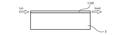
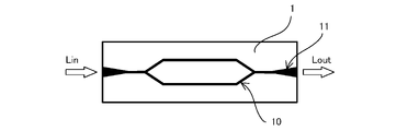
- FIGS. 1 and 2 the substrate 1 such as lithium niobate (LN) is thinned to a thickness of 20 ⁇ m or less, and the optical waveguide 10 is formed on the substrate 1.
- FIG. 1 is a plan view of an optical waveguide element constituting an optical modulator, and electrodes such as a modulation electrode are omitted for simplification.
- FIG. 2 is a side view of FIG. 1.
- the substrate 1 to be a thin plate is joined to the holding substrate 2 via the adhesive layer 3. Lin indicates incident light, and Lout indicates emitted light.
- the new thin plate structure optical modulator In order to use it as an integrated LN optical modulator such as HB-CDM (High Bandwidth-Coherent Driver Modulator), it is essential to reduce the size of the optical waveguide element, and to reduce the drive voltage, the cross-sectional structure of the optical waveguide is further reduced. There must be. Therefore, as shown in FIG. 3, in the new thin plate structure optical modulator, it is necessary to thin the substrate 1 such as lithium niobate (LN) to a thickness of 2 ⁇ m or less, and the adhesive layer having a significantly different coefficient of thermal expansion is required. It is required to directly bond to the holding substrate 2 without using the above.
- LN lithium niobate
- the optical mode field diameter of the optical waveguide 10 is about 1 ⁇ m, which is larger than the optical mode field diameter of 10 ⁇ m of the optical fiber. Therefore, the light loss at the connection between the optical waveguide element and the optical fiber at the incident part or the exit part is about 0.5 dB at one end of the conventional thin plate structure (thickness about 10 ⁇ m) optical modulator, but it is new.
- the optical modulator of the thin plate structure of is significantly increased to 14 dB or more at one end.
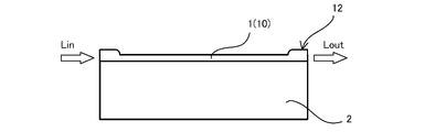
- Non-Patent Document 1 In the case of an optical modulator using a semiconductor material in order to reduce the optical loss due to the coupling with the optical fiber, as shown in FIG. 4 or FIG. A method of converting the optical mode field diameter (MFD) by providing a vertical tapered optical waveguide (see reference numeral 12 in FIG. 5) has been proposed. (See Non-Patent Document 1)
- the problem to be solved by the present invention is to solve the above-mentioned problems and to provide an optical waveguide element which is compact, has low light loss, and has long-term stability. Further, it is to provide an optical modulation device and an optical transmission device using the optical waveguide element.
- the optical waveguide element of the present invention, the optical modulation device using the optical waveguide element, and the optical transmission device have the following technical features.
- the optical waveguide A is formed on the first substrate, and at the end of the first substrate, an incident portion for incident the light wave on the optical waveguide A or an exit portion for emitting the light wave from the optical waveguide A is provided.
- the optical waveguide B is formed on the second substrate, and the second substrate has an optical waveguide that modulates the light wave propagating in the optical waveguide B, and at least the optical waveguide A is provided.
- a part of the optical waveguide element is characterized by having a conversion unit that converts the optical mode field diameter.
- optical waveguide element according to (1) above is characterized in that the optical mode field diameter of the light wave converted by the conversion unit is in the range of 2 ⁇ m or more and 5 ⁇ m or less.
- the thickness of the second substrate is 2 ⁇ m or less.
- the optical waveguide A and the optical waveguide B in the optical waveguide A are connected and formed on the first substrate.
- the connected optical waveguide to be made is characterized in that it is formed by either ion implantation, ion exchange, or an ultrashort pulse laser.
- either the first substrate or the second substrate is provided with a phase adjusting electrode. It is a feature.
- a bent portion in which the traveling direction of the light wave rotates 180 degrees is formed in either the optical waveguide A or the optical waveguide B. It is characterized by being done.
- the optical waveguide element according to any one of (1) to (6) above is housed in a housing, and the housing is provided with an optical fiber that inputs or outputs light waves to the optical waveguide. It is a modulation device.
- the optical modulation section of the optical waveguide element is provided with a modulation electrode, and an electronic circuit for amplifying a modulation signal input to the modulation electrode is installed inside the housing. It is characterized by having.
- An optical transmission device comprising the optical modulation device according to (7) or (8) above, and an electronic circuit that outputs a modulation signal that causes the optical modulation device to perform a modulation operation.
- FIG. 7 It is sectional drawing in FIG. 7 one-dot chain line AA'. It is a figure which shows the change of the coupling efficiency when the mode field diameter of a conversion part is changed. It is a side view which shows the 2nd Embodiment of the optical waveguide element of this invention. It is a top view which shows the 3rd Embodiment of the optical waveguide element of this invention. It is a top view which shows the 4th Embodiment of the optical waveguide element of this invention. It is a top view which shows the 5th Embodiment of the optical waveguide element of this invention. It is a top view explaining the optical modulation device and the optical transmission apparatus of this invention.
- the material 1 of the second substrate used in the optical waveguide element of the present invention is composed of a material having an electro-optical effect, and in particular, lithium niobate (LN) or lithium tantalate (LT), PLZT (titanium zirconate). Substrates such as lead acid lanthanum) or vapor deposition films made of these materials can be used. Further, various materials such as semiconductor materials and organic materials can also be used as optical waveguides.
- a rib-type optical waveguide having a convex portion corresponding to the optical waveguide is formed on the substrate, such as etching a substrate 1 other than the optical waveguide or forming grooves on both sides of the optical waveguide. It is possible to use it. Further, it is also possible to further increase the refractive index of the optical waveguide by diffusing Ti or the like on the substrate surface by a heat diffusion method, a proton exchange method, or the like in accordance with the rib-type optical waveguide.
- the thickness of the second substrate (thin plate) on which the optical waveguide 10 is formed is set to 2 ⁇ m or less in order to match the speed between the microwave and the light wave of the modulated signal.
- the height of the rib-type optical waveguide is set to 1 ⁇ m or less, more preferably 0.4 ⁇ m or less. It is also possible to form a vapor phase growth film on the first substrate 2 which is a holding substrate and process the film into the shape of an optical waveguide.
- the first substrate 2 as a holding substrate is directly bonded to the second substrate 1 on which the optical waveguide is formed, without using a resin layer (adhesive layer).
- the first substrate 2 has a lower refractive index than the second substrate and has a coefficient of thermal expansion close to that of an optical waveguide or the like, for example, a substrate containing an oxide layer such as quartz or glass (referred to as “glass material”). Is preferably used.
- a composite substrate in which a silicon oxide layer is formed on a silicon substrate, which is abbreviated as SOI or LNOI, or a silicon oxide layer is formed on an LN substrate can also be used.
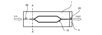
- the feature of the optical waveguide element of the present invention is that, as shown in FIGS. 7 and 8, an embedded optical waveguide A (20) is formed at an end portion of a first substrate (for example, a glass substrate). It is a feature. A part or all of the optical waveguide A functions as a conversion unit that changes the optical mode field diameter of the propagating light wave. Then, as an example, after the second substrate (for example, LN substrate) is directly bonded to the first substrate on which the optical waveguide A is formed, the second substrate is polished to 2 ⁇ m or less to be thinned, and then dry or wet. A rib-type optical waveguide B (10) can be formed on the second substrate by the etching method according to the above method.
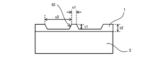
- FIG. 9 shows a cross-sectional view taken along the alternate long and short dash line AA'in FIG.
- the width s1 of the optical waveguide is set in the range of 0.2 to 2.0 ⁇ m
- the height t1 is set in the range of 0.2 to 2.0 ⁇ m.
- the distance s2 to the protrusion (the substrate portion remaining without etching) of the substrate adjacent to the optical waveguide is 5.0 to 50.0 ⁇ m
- the thickness of the second substrate 1 is 0.5 to 2.0 ⁇ m. Is set to.
- the optical mode field diameter (10 ⁇ m) of the optical fiber and the optical mode field diameter (1 ⁇ m) of the LN substrate having the optical modulator are rapidly increased. It is possible to prevent an increase in light loss due to such changes.
- the exit side end of the rib-type optical waveguide (10) has a tapered structure, so that the mode can be smoothly transferred to the optical waveguide formed on the first substrate.
- the optical mode field diameter w2 of the second substrate is 0.5 ⁇ m, 1.0 ⁇ m, and 2.0 ⁇ m
- the optical mode field diameter w1 of the first substrate is 1.0 ⁇ m to 10.0 ⁇ m.
- the optical mode field diameter is simply calculated by the difference in the optical mode field diameter as the average of the optical mode field diameters in the vertical direction and the horizontal direction.
- each graph is standardized based on the peak value.
- the optical mode field diameter is set to include a region where w1 is 2 ⁇ m or more and 5 ⁇ m or less, thereby preventing a significant decrease in coupling efficiency. This can lead to a reduction in light loss. Further, since a steep change in the optical mode field diameter leads to an increase in optical loss, it is expected that the optical loss will be further reduced by gently changing w1 of the optical waveguide A and w2 of the optical waveguide B.
- w1 of the optical waveguide A (20) is larger than w2 of the optical waveguide B (10), and the optical waveguide A and the optical waveguide B are at least when the first substrate is viewed in a plan view. It is desirable that they overlap. However, when the evanescent wave of each optical waveguide is used, the optical waveguide A and the optical waveguide B do not have to overlap each other within the range of optical coupling. Further, it is desirable that the refractive index n1 of the optical waveguide A (20) is smaller than the refractive index n2 of the optical waveguide B (10).
- Examples of the method for forming the embedded optical waveguide A on the first substrate (glass substrate) include ion exchange, ion implantation, and ultrashort pulse laser drawing.
- ion exchange when a mask pattern is formed on a glass substrate such as soda glass with a metal film such as titanium and immersed in a potassium nitrate melt at 300 to 400 ° C., only the opening portion of the metal film is selectively ion exchanged.
- the optical waveguide is formed.
- the refractive index can be increased by about 0.01 to 0.1 depending on conditions such as immersion temperature, time, and applied voltage. K, Ag, Tl and the like can be used for ion exchange.
- Such a configuration can have a larger difference in refractive index than an optical waveguide in which titanium is thermally diffused in lithium niobate.
- the optical mode field diameter of the glass substrate can be made smaller than the optical mode field diameter (10 ⁇ m) of the optical fiber. Therefore, the optical mode field diameter of the substrate can be set to the above-mentioned region of 2 ⁇ m or more and 5 ⁇ m or less, so that it is possible to prevent a significant decrease in the coupling efficiency with the optical fiber.
- an optical waveguide can be formed on one surface of the first substrate. After polishing the surface of the glass substrate, it is directly bonded to the LN substrate, and then the LN substrate is polished to 2 ⁇ m or less. After forming a rib-type waveguide by dry etching on the LN substrate, a gold electrode is formed by a plating method.
- the condensed irradiation of a femtosecond laser induces a structural change inside the glass, so that the refractive index changes and an optical waveguide is formed. It is possible to increase the refractive index near the focal point of the laser beam by about 0.01 depending on the conditions such as pulse width, repetition frequency, and pulse energy.
- the silicon and oxygen networks that make up ordinary silica glass are dominated by 6- or 5-membered rings, but the network at the site irradiated with the ultrashort pulse laser has a reduced number of members, and the 3-membered ring, The number of 4-membered rings increases.
- the content of the 3- or 4-membered ring of silicon and oxygen in the silica glass in the optical waveguide formed by the focused irradiation of the femtosecond laser is the other of the substrate on which the optical waveguide is formed. It will be larger than the content in the portion.
- the optical waveguide with an increased 3-membered ring and 4-membered ring has an improved density and an increased mechanical strength as compared with other parts where the membered ring does not change.
- the optical waveguide is formed by an ultrashort pulse laser
- the optical waveguide is limited to the focal point of the laser light. Therefore, the optical waveguide of the LN substrate having the optical modulation unit and the optical waveguide formed on the glass substrate are three-dimensionally connected. It is also possible to provide an optical waveguide element with lower loss.
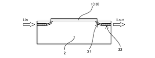
- the optical waveguide (22) and the connected optical waveguide (21) can also be formed by an ultrashort pulse laser or the above-mentioned ion exchange or ion implantation.
- the connected optical waveguide (21) is three-dimensionally formed in the thickness direction of the first substrate (glass substrate) (2) as shown in FIG. 11, the light loss is reduced and the mechanical intensity is reduced.
- at least the connected optical waveguide (21) may be formed by an ultrashort pulse laser to increase the number of 3-membered rings and 4-membered rings.
- the refractive index of the connected optical waveguide (21) may be formed so as to gradually increase from the optical waveguide (10) side to the optical waveguide (22) side.
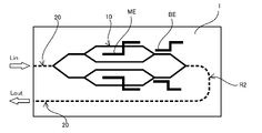
- FIG. 12 is a structure for reducing light loss only in the light input / output portion (the portion of the optical waveguide (20)).
- FIG. 13 has a structure in which a light input / output portion, a 180 ° bent portion (R2), and a straight line portion connecting the bent portion to the exit portion are formed on the first substrate to reduce light loss.
- FIG. 14 shows a structure in which the light input / output portion, the 180 ° bent portion, the straight portion, and the Mach-Zehnder branch portion are formed on the first substrate except for the optical modulation portion to reduce the light loss. It has become.
- Reference numeral MEs shown in FIGS. 12 to 14 are traveling wave type modulation electrodes, and reference numeral BE is a bias electrode for phase adjustment.
- the phase adjusting electrode BE is provided on the second substrate (LN substrate), it is composed of a DC bias electrode.
- the electrode BE when the electrode BE is provided on the first substrate (glass substrate), it becomes a heating electrode using the thermo-optical effect.
- the incident portion (Lin) and the exit portion (Lout) in FIGS. 12 to 14 may be interchanged. In this case, the positions of the modulation electrode and the bias electrode are appropriately changed.
- the transmission distance of the optical waveguide on the incident side is long, it is desirable that the polarization state of light is maintained.
- an optical transmission device OTA by connecting an electronic circuit (digital signal processor DSP) that outputs a modulation signal that causes the optical modulation device MD to perform a modulation operation to the optical modulation device MD. Since the modulation signal applied to the optical waveguide element needs to be amplified, the driver circuit DRV is used.
- the driver circuit DRV and the digital signal processor DSP can be arranged outside the housing 8, but can also be arranged inside the housing 8. In particular, by arranging the driver circuit DRV in the housing, it is possible to further reduce the propagation loss of the modulated signal from the driver circuit.
- an optical waveguide device which is compact, has low light loss, and has long-term stability. Further, it becomes possible to provide an optical modulation device and an optical transmission device using the optical waveguide element.
- Second board 2 First board 10 Optical waveguide B 20 Optical Waveguide A (including a part or all of the optical mode field diameter converter)
Landscapes
- Physics & Mathematics (AREA)
- Nonlinear Science (AREA)
- General Physics & Mathematics (AREA)
- Optics & Photonics (AREA)
- Engineering & Computer Science (AREA)
- Microelectronics & Electronic Packaging (AREA)
- Chemical & Material Sciences (AREA)
- Ceramic Engineering (AREA)
- Crystallography & Structural Chemistry (AREA)
- Optical Integrated Circuits (AREA)
- Optical Modulation, Optical Deflection, Nonlinear Optics, Optical Demodulation, Optical Logic Elements (AREA)
Abstract
L'objectif de la présente invention est de fournir un élément de guide d'ondes optique compact et à faible perte de lumière ayant une stabilité à long terme. L'invention concerne un élément de guide d'ondes optique caractérisé en ce qu'il possède un guide d'ondes optique A (20) formé dans un premier substrat (2), ayant une partie d'incidence à travers laquelle une onde lumineuse est incidente sur le guide d'ondes optique A ou une partie d'émission à travers laquelle une onde lumineuse est émise à partir du guide d'ondes optique A dans une partie d'extrémité du premier substrat, ayant un guide d'ondes optique B (10) formé dans un second substrat (1), ayant une partie de modulation optique pour moduler une onde lumineuse se propageant à travers le guide d'ondes optique B dans le second substrat, et ayant une partie de conversion (20) pour convertir un diamètre de champ de mode optique dans au moins une partie du guide d'ondes optique A (20).
Priority Applications (2)
| Application Number | Priority Date | Filing Date | Title |
|---|---|---|---|
| US18/021,342 US12504655B2 (en) | 2020-09-30 | 2021-09-28 | Optical waveguide element, and optical modulation device and optical transmission apparatus that use same |
| CN202180040909.8A CN115698793A (zh) | 2020-09-30 | 2021-09-28 | 光波导元件及使用了该光波导元件的光调制器件以及光发送装置 |
Applications Claiming Priority (2)
| Application Number | Priority Date | Filing Date | Title |
|---|---|---|---|
| JP2020165005A JP7484631B2 (ja) | 2020-09-30 | 2020-09-30 | 光導波路素子及びそれを用いた光変調デバイス並びに光送信装置 |
| JP2020-165005 | 2020-09-30 |
Publications (1)
| Publication Number | Publication Date |
|---|---|
| WO2022071283A1 true WO2022071283A1 (fr) | 2022-04-07 |
Family
ID=80950448
Family Applications (1)
| Application Number | Title | Priority Date | Filing Date |
|---|---|---|---|
| PCT/JP2021/035550 Ceased WO2022071283A1 (fr) | 2020-09-30 | 2021-09-28 | Élément de guide d'ondes optique, et dispositif de modulation optique et dispositif de transmission optique qui l'utilisent |
Country Status (4)
| Country | Link |
|---|---|
| US (1) | US12504655B2 (fr) |
| JP (1) | JP7484631B2 (fr) |
| CN (1) | CN115698793A (fr) |
| WO (1) | WO2022071283A1 (fr) |
Cited By (1)
| Publication number | Priority date | Publication date | Assignee | Title |
|---|---|---|---|---|
| WO2024201876A1 (fr) * | 2023-03-30 | 2024-10-03 | 住友大阪セメント株式会社 | Élément de guide d'ondes optique et dispositif de modulation optique l'utilisant, et dispositif de transmission optique |
Citations (6)
| Publication number | Priority date | Publication date | Assignee | Title |
|---|---|---|---|---|
| JP2000214341A (ja) * | 1999-01-21 | 2000-08-04 | Samsung Electronics Co Ltd | モ―ド形状変換器、その製造方法及びモ―ド形状変換器を用いた集積光学素子 |
| JP2006284961A (ja) * | 2005-03-31 | 2006-10-19 | Sumitomo Osaka Cement Co Ltd | 光変調器 |
| WO2009106139A1 (fr) * | 2008-02-29 | 2009-09-03 | Pirelli & C. S.P.A. | Transformateur de mode optique permettant en particulier de coupler une fibre optique et un guide d'onde à forte différence d'indice |
| JP2014191301A (ja) * | 2013-03-28 | 2014-10-06 | Fujitsu Ltd | スポットサイズ変換器、その製造方法及び光集積回路装置 |
| JP2019095698A (ja) * | 2017-11-27 | 2019-06-20 | 富士通オプティカルコンポーネンツ株式会社 | 光モジュール及び光変調器 |
| WO2019180922A1 (fr) * | 2018-03-23 | 2019-09-26 | 日本碍子株式会社 | Substrat composite pour dispositif électro-optique |
Family Cites Families (41)
| Publication number | Priority date | Publication date | Assignee | Title |
|---|---|---|---|---|
| US5393371A (en) * | 1989-12-18 | 1995-02-28 | Litton Systems, Inc. | Integrated optics chips and laser ablation methods for attachment of optical fibers thereto for LiNbO3 substrates |
| JP2001154164A (ja) * | 1999-11-25 | 2001-06-08 | Nec Corp | 光変調器および光変調方法 |
| US7295742B2 (en) * | 2002-05-31 | 2007-11-13 | Matsushita Electric Industrial Co., Ltd. | Optical element and method for producing the same |
| JP2004219751A (ja) * | 2003-01-15 | 2004-08-05 | Matsushita Electric Ind Co Ltd | 光導波路デバイスならびにそれを用いた光導波路レーザおよびそれを備えた光学装置 |
| CN1723401B (zh) * | 2003-05-23 | 2010-12-01 | 松下电器产业株式会社 | 光器件和光器件制造方法以及光集成器件 |
| EP1657588B1 (fr) * | 2003-08-21 | 2015-03-04 | NGK Insulators, Ltd. | Dispositif de guide d'ondes optique et modulateur optique de type a onde itinerante |
| JP4146788B2 (ja) * | 2003-12-10 | 2008-09-10 | 日本電信電話株式会社 | 光導波路接続モジュールおよびその導波路作製方法 |
| JP4594744B2 (ja) * | 2005-01-14 | 2010-12-08 | 富士通オプティカルコンポーネンツ株式会社 | 光通信デバイス及び光デバイス |
| JP4658658B2 (ja) * | 2005-03-29 | 2011-03-23 | 住友大阪セメント株式会社 | 光変調器 |
| JP2007133135A (ja) * | 2005-11-10 | 2007-05-31 | Ngk Insulators Ltd | 光導波路デバイス |
| JP4183716B2 (ja) * | 2006-03-29 | 2008-11-19 | 住友大阪セメント株式会社 | 光導波路素子 |
| WO2008099950A1 (fr) * | 2007-02-14 | 2008-08-21 | Ngk Insulators, Ltd. | Composant de modulateur optique et modulateur optique |
| US8285092B2 (en) * | 2007-03-20 | 2012-10-09 | Nec Corporation | Optical waveguide and spot size converter using the same |
| JP4701232B2 (ja) * | 2007-12-28 | 2011-06-15 | 住友大阪セメント株式会社 | 光変調器 |
| JP5006933B2 (ja) * | 2008-01-10 | 2012-08-22 | 日本電信電話株式会社 | 光遅延干渉回路 |
| JP2009217009A (ja) * | 2008-03-11 | 2009-09-24 | Ngk Insulators Ltd | 高調波発生素子 |
| JP5254855B2 (ja) * | 2008-03-28 | 2013-08-07 | 日本碍子株式会社 | 進行波型光変調器 |
| JP4388987B2 (ja) * | 2008-03-31 | 2009-12-24 | 住友大阪セメント株式会社 | マッハツェンダー導波路型光変調器 |
| WO2010082673A1 (fr) * | 2009-01-16 | 2010-07-22 | 日本碍子株式会社 | Guide d'ondes optique ramifié, substrat de guide d'ondes optique et modulateur optique |
| JP5494400B2 (ja) * | 2010-09-30 | 2014-05-14 | 住友大阪セメント株式会社 | 光導波路素子 |
| JP5660095B2 (ja) * | 2012-08-31 | 2015-01-28 | 住友大阪セメント株式会社 | 光変調器 |
| US9804348B2 (en) * | 2013-07-04 | 2017-10-31 | Mellanox Technologies, Ltd. | Silicon photonics connector |
| WO2015098854A1 (fr) * | 2013-12-27 | 2015-07-02 | 株式会社フジクラ | Procede de production destine a des dispositifs optiques |
| CN105900298A (zh) * | 2014-01-14 | 2016-08-24 | 日本碍子株式会社 | 外部谐振器型发光装置 |
| CN104166182A (zh) * | 2014-08-25 | 2014-11-26 | 北京大学 | 一种波导模式转换器 |
| US10852492B1 (en) * | 2014-10-29 | 2020-12-01 | Acacia Communications, Inc. | Techniques to combine two integrated photonic substrates |
| JP2018097159A (ja) * | 2016-12-14 | 2018-06-21 | 住友大阪セメント株式会社 | 薄板ln光制御デバイス |
| US10948658B2 (en) * | 2017-02-27 | 2021-03-16 | Corning Optical Communications LLC | Optical interconnection assemblies, glass interconnection substrates, and methods of making an optical connection |
| WO2018225820A1 (fr) * | 2017-06-07 | 2018-12-13 | 日本電信電話株式会社 | Structure de connexion pour puce de guide d'ondes optique |
| JP7047469B2 (ja) * | 2018-03-05 | 2022-04-05 | 住友大阪セメント株式会社 | 光変調器 |
| JP7073963B2 (ja) * | 2018-07-24 | 2022-05-24 | 住友大阪セメント株式会社 | 光導波路素子 |
| US10589255B1 (en) * | 2018-10-11 | 2020-03-17 | Imam Abdulrahman Bin Faisal University | Tantalum vanadate nanorods and methods of their make and use |
| WO2020245867A1 (fr) * | 2019-06-03 | 2020-12-10 | 日本電信電話株式会社 | Structure de connexion de fibre optique |
| JP7364929B2 (ja) * | 2019-07-08 | 2023-10-19 | 日本電信電話株式会社 | 光ファイバアレイの接続方法 |
| US10921682B1 (en) * | 2019-08-16 | 2021-02-16 | Kvh Industries, Inc. | Integrated optical phase modulator and method of making same |
| WO2021044517A1 (fr) * | 2019-09-03 | 2021-03-11 | 日本電信電話株式会社 | Composant de guides d'ondes optiques |
| WO2021111525A1 (fr) * | 2019-12-03 | 2021-06-10 | 日本電信電話株式会社 | Élément optique et son procédé de fabrication |
| CN111061009B (zh) * | 2019-12-30 | 2022-06-28 | 腾讯科技(深圳)有限公司 | 悬空光波导及其制备方法 |
| JP7526610B2 (ja) * | 2020-08-13 | 2024-08-01 | 富士通オプティカルコンポーネンツ株式会社 | 光導波路デバイス |
| JP7540274B2 (ja) * | 2020-09-30 | 2024-08-27 | 住友大阪セメント株式会社 | 光導波路素子及びそれを用いた光変調デバイス並びに光送信装置 |
| JP7528834B2 (ja) * | 2021-03-24 | 2024-08-06 | 住友大阪セメント株式会社 | 光導波路素子、光変調器、光変調モジュール、及び光送信装置 |
-
2020
- 2020-09-30 JP JP2020165005A patent/JP7484631B2/ja active Active
-
2021
- 2021-09-28 WO PCT/JP2021/035550 patent/WO2022071283A1/fr not_active Ceased
- 2021-09-28 CN CN202180040909.8A patent/CN115698793A/zh active Pending
- 2021-09-28 US US18/021,342 patent/US12504655B2/en active Active
Patent Citations (6)
| Publication number | Priority date | Publication date | Assignee | Title |
|---|---|---|---|---|
| JP2000214341A (ja) * | 1999-01-21 | 2000-08-04 | Samsung Electronics Co Ltd | モ―ド形状変換器、その製造方法及びモ―ド形状変換器を用いた集積光学素子 |
| JP2006284961A (ja) * | 2005-03-31 | 2006-10-19 | Sumitomo Osaka Cement Co Ltd | 光変調器 |
| WO2009106139A1 (fr) * | 2008-02-29 | 2009-09-03 | Pirelli & C. S.P.A. | Transformateur de mode optique permettant en particulier de coupler une fibre optique et un guide d'onde à forte différence d'indice |
| JP2014191301A (ja) * | 2013-03-28 | 2014-10-06 | Fujitsu Ltd | スポットサイズ変換器、その製造方法及び光集積回路装置 |
| JP2019095698A (ja) * | 2017-11-27 | 2019-06-20 | 富士通オプティカルコンポーネンツ株式会社 | 光モジュール及び光変調器 |
| WO2019180922A1 (fr) * | 2018-03-23 | 2019-09-26 | 日本碍子株式会社 | Substrat composite pour dispositif électro-optique |
Cited By (1)
| Publication number | Priority date | Publication date | Assignee | Title |
|---|---|---|---|---|
| WO2024201876A1 (fr) * | 2023-03-30 | 2024-10-03 | 住友大阪セメント株式会社 | Élément de guide d'ondes optique et dispositif de modulation optique l'utilisant, et dispositif de transmission optique |
Also Published As
| Publication number | Publication date |
|---|---|
| CN115698793A (zh) | 2023-02-03 |
| JP2022056982A (ja) | 2022-04-11 |
| US20230305325A1 (en) | 2023-09-28 |
| JP7484631B2 (ja) | 2024-05-16 |
| US12504655B2 (en) | 2025-12-23 |
Similar Documents
| Publication | Publication Date | Title |
|---|---|---|
| WO2008099950A1 (fr) | Composant de modulateur optique et modulateur optique | |
| JP7295467B2 (ja) | 光学素子及びその製造方法 | |
| WO2022071283A1 (fr) | Élément de guide d'ondes optique, et dispositif de modulation optique et dispositif de transmission optique qui l'utilisent | |
| JP2019105808A (ja) | 光学素子およびその製造方法 | |
| JPH03150509A (ja) | 導波路基板と光ファイバの接続方法及び該方法の実施に使用する紫外光遮断機能付き反射防止膜 | |
| JPH0996731A (ja) | 導波路形光デバイス | |
| CN120266046A (zh) | 光波导元件、光调制器及光发送装置 | |
| CN118732154A (zh) | 光波导元件、使用光波导元件的光调制器件及光发送装置 | |
| US12455489B2 (en) | Electromagnetic radiation frequency converter and light source comprising the same | |
| JP7553868B2 (ja) | 波長変換装置及び波長変換装置の製造方法 | |
| JPH06289347A (ja) | 光導波路素子とその製造方法 | |
| JP5013377B2 (ja) | 光デバイス | |
| JP3735685B2 (ja) | 集積型光導波路素子 | |
| JP2008122762A (ja) | 光導波路パッケージ、光導波路パッケージ用筐体、光導波路パッケージの製造方法、および光導波路パッケージの特性調整方法 | |
| US20240255784A1 (en) | Optical Waveguide Device, and Optical Modulation Device and Optical Transmission Apparatus Using Same | |
| DK181086B1 (en) | Electromagnetic radiation frequency converter and light source comprising same | |
| JPH01201627A (ja) | 導波路型光スイツチ | |
| JP7218652B2 (ja) | 光制御素子 | |
| US20240231002A1 (en) | Optical waveguide element, and optical transmission apparatus and optical modulation device using same | |
| JPH11337892A (ja) | 光導波路素子およびその製造方法 | |
| WO2022130515A1 (fr) | Guide d'ondes optique hybride tridimensionnel et son procédé de production | |
| HK40082347A (en) | Electromagnetic radiation frequency converter and light source comprising same | |
| CN118746899A (zh) | 高集成双层薄膜铌酸锂光子处理系统及其制备方法 | |
| WO2023053404A1 (fr) | Élément de guide d'ondes optique, et dispositif de modulation optique et appareil de transmission optique qui l'utilisent | |
| Srisanit | Laser direct write optical waveguides for optical interconnection and optical isolation |
Legal Events
| Date | Code | Title | Description |
|---|---|---|---|
| 121 | Ep: the epo has been informed by wipo that ep was designated in this application |
Ref document number: 21875584 Country of ref document: EP Kind code of ref document: A1 |
|
| NENP | Non-entry into the national phase |
Ref country code: DE |
|
| 122 | Ep: pct application non-entry in european phase |
Ref document number: 21875584 Country of ref document: EP Kind code of ref document: A1 |