WO2023175990A1 - Euv透過膜の製造方法及びペリクル - Google Patents
Euv透過膜の製造方法及びペリクル Download PDFInfo
- Publication number
- WO2023175990A1 WO2023175990A1 PCT/JP2022/012918 JP2022012918W WO2023175990A1 WO 2023175990 A1 WO2023175990 A1 WO 2023175990A1 JP 2022012918 W JP2022012918 W JP 2022012918W WO 2023175990 A1 WO2023175990 A1 WO 2023175990A1
- Authority
- WO
- WIPO (PCT)
- Prior art keywords
- substrate
- cavity
- euv
- film
- layer
- Prior art date
- Legal status (The legal status is an assumption and is not a legal conclusion. Google has not performed a legal analysis and makes no representation as to the accuracy of the status listed.)
- Ceased
Links
Images





Classifications
-
- G—PHYSICS
- G03—PHOTOGRAPHY; CINEMATOGRAPHY; ANALOGOUS TECHNIQUES USING WAVES OTHER THAN OPTICAL WAVES; ELECTROGRAPHY; HOLOGRAPHY
- G03F—PHOTOMECHANICAL PRODUCTION OF TEXTURED OR PATTERNED SURFACES, e.g. FOR PRINTING, FOR PROCESSING OF SEMICONDUCTOR DEVICES; MATERIALS THEREFOR; ORIGINALS THEREFOR; APPARATUS SPECIALLY ADAPTED THEREFOR
- G03F1/00—Originals for photomechanical production of textured or patterned surfaces, e.g., masks, photo-masks, reticles; Mask blanks or pellicles therefor; Containers specially adapted therefor; Preparation thereof
- G03F1/62—Pellicles, e.g. pellicle assemblies, e.g. having membrane on support frame; Preparation thereof
-
- G—PHYSICS
- G03—PHOTOGRAPHY; CINEMATOGRAPHY; ANALOGOUS TECHNIQUES USING WAVES OTHER THAN OPTICAL WAVES; ELECTROGRAPHY; HOLOGRAPHY
- G03F—PHOTOMECHANICAL PRODUCTION OF TEXTURED OR PATTERNED SURFACES, e.g. FOR PRINTING, FOR PROCESSING OF SEMICONDUCTOR DEVICES; MATERIALS THEREFOR; ORIGINALS THEREFOR; APPARATUS SPECIALLY ADAPTED THEREFOR
- G03F1/00—Originals for photomechanical production of textured or patterned surfaces, e.g., masks, photo-masks, reticles; Mask blanks or pellicles therefor; Containers specially adapted therefor; Preparation thereof
- G03F1/62—Pellicles, e.g. pellicle assemblies, e.g. having membrane on support frame; Preparation thereof
- G03F1/64—Pellicles, e.g. pellicle assemblies, e.g. having membrane on support frame; Preparation thereof characterised by the frames, e.g. structure or material, including bonding means therefor
Definitions
- the present invention relates to a method for manufacturing an EUV transparent membrane and a pellicle.
- Patent Document 1 Japanese Patent No. 68588157 discloses that the core layer includes a material that is substantially transparent to EUV radiation, such as (poly)Si, and a cap layer that includes a material that absorbs IR radiation.
- a pellicle membrane is disclosed.
- a poly-Si-based pellicle film is set to a thickness that maintains film strength, the EUV transmittance cannot reach the target of 90%, and it is still not practical.
- CNT-based pellicle membranes have also been developed (for example, Patent Document 2 (Japanese Unexamined Patent Publication No. 2018-194840)), and higher EUV transmittance is expected.
- CNT-based pellicle membranes lack durability against the environment in which the pellicle is used (low-pressure hydrogen atmosphere), and if the pellicle membrane is coated with metal to provide durability, the EUV transmittance decreases and a practical level of transmittance is not achieved. The reality is that this is not possible.
- Non-Patent Document 1 (Dario L. Goldfarb, "Fabrication of a full size EUV pellicle based on silicon nitride", Volume 31, Issue 12, PHOTOMASK, SPIE, 2015)
- a SiNx free-standing film is manufactured as a pellicle film.
- a method is disclosed. The basic method is as follows. First, a SiNx film to be a pellicle film is formed on both sides of a Si substrate (step A). Next, a reactive ion etching (RIE) mask for etching the formed SiNx film is formed on only one side (Step B).
- RIE reactive ion etching
- Step C Part of the SiNx is removed by RIE to expose the Si substrate.
- Step D the outer shape of the Si substrate is diced.
- the Si substrate is wet-etched to form a self-supporting SiNx film (step E).
- Patent No. 6858817 Japanese Patent Application Publication No. 2018-194840
- FIGS. 4A and 4B An example of such a conventional manufacturing process is shown in FIGS. 4A and 4B.
- a substrate 110 such as a Si wafer is prepared (FIG. 4A(a)).
- Mask layers 112 such as two layers of SiO 2 are formed on both sides of this substrate 110 .
- a resist is applied to one or both sides of the substrate 110, and exposure and development are performed so that a resist hole of a predetermined size is formed on one side to form a resist mask (not shown) for etching.
- a resist mask (not shown) for etching.
- the exposed portion of the mask layer 112 is etched away to form an opening corresponding to the cavity region C (FIG. 4A(c)).
- the substrate 110 is etched with an etching solution such as TMAH (tetramethylammonium hydroxide) solution to thin the cavity region C of the substrate 110 to a desired thickness, thereby forming a cavity 114 ( Figure 4A(d)).
- TMAH tetramethylammonium hydroxide
- the mask layer 112 present on the surface opposite to the cavity 114 is removed by etching to obtain a cavity substrate 115 (FIG. 4B(e)).
- An EUV transmission film 116 is formed on the surface of the cavity substrate 115 opposite to the cavity 114 (FIG. 4B(f)).
- the substrate 110 corresponding to the portion to be made into a self-supporting film is removed by etching to make the EUV transmitting film 116 into a self-supporting film (FIG. 4B(g)).
- a pellicle 118 having a frame 117 including the substrate 110 and the mask layer 112 left in a frame shape, and the EUV transmitting film 116 is obtained.
- the inner edge 112a of the frame-shaped mask layer 112 remains in the shape of an eave extending toward the cavity 114, as shown in FIGS. 4B(g) and 4C.
- the substrate 110 such as a Si wafer for forming the cavity 114 is etched from the bottom surface, as the etching progresses upward in the figure, side etching is also performed in the lateral direction. If the mask layer 112 is left in an eave-like state extending toward the cavity 114 in this way, the eave-like inner edge 112a, which is weak in strength, will be damaged and particles (dust) will be generated. It tends to adhere to the EUV transparent membrane 116.
- the particle portion blocks EUV light during exposure, resulting in exposure failure in which the mask pattern is not accurately transferred.
- the present inventors have recently formed an EUV-transmissive film on the surface of the substrate on the cavity side, and etched away the substrate from the surface opposite to the cavity to make the EUV-transmissive film into a self-supporting film, thereby making the mask layer transparent to the cavity. It has been found that a high-quality EUV-transmissive membrane or pellicle can be manufactured by an efficient method that is less likely to generate particles by avoiding particles remaining in the eaves-like shape extending toward the surface.
- an object of the present invention is to manufacture a high-quality EUV transmitting film or pellicle using an efficient method that is less likely to generate particles by avoiding the mask layer remaining in the eaves shape extending toward the cavity. There is a particular thing.
- a method for manufacturing an EUV-transmissive membrane including:
- preparing a substrate having a first side and a second side covering the entire area of the first surface and the peripheral area other than the cavity area located at the center of the second surface with a mask layer; partially etching away the substrate exposed in the cavity region to form a cavity; etching away the mask layer covering the first surface and the mask layer covering the peripheral region of the second surface; forming an EUV-transmissive film on the cavity-side surface of the substrate; etching away the substrate from the first surface until the EUV-transmissive film is exposed on a side opposite to the cavity, thereby forming the EUV-transmissive film in the cavity region into a self-supporting film;
- a method for manufacturing an EUV-transmissive membrane including:
- a substrate having a first surface and a second surface and having a cavity in the center; a mask layer covering a second surface of the substrate; an EUV-transmissive film that continuously covers the surface of the mask layer and the inner surface of the cavity of the substrate and is exposed as a free-standing film forming a bottom surface of the cavity at the same height as the first surface;
- a pellicle is provided with a
- a substrate having a first surface and a second surface and having a cavity in the center; an EUV-transmissive film that continuously covers a second surface of the substrate and an inner surface of the cavity and is exposed as a free-standing film forming a bottom surface of the cavity at the same height as the first surface;
- a pellicle is provided with a
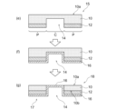
- FIG. 3 is a diagram illustrating an example of the first half of a method for manufacturing an EUV transparent membrane according to one embodiment of the present invention.
- 1A is a diagram illustrating an example of a latter half step following FIG. 1A in a method for manufacturing an EUV transmission membrane according to one embodiment of the present invention.
- FIG. 1A is a diagram illustrating another example of the latter half of the process following FIG. 1A in the method for manufacturing an EUV permeable membrane according to one embodiment of the present invention.
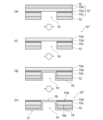
- FIG. It is a figure which shows another example of the first half process in the manufacturing method of the EUV transmission membrane by this invention.
- 2A is a diagram illustrating an example of the latter half of the process following FIG. 2A in the method for manufacturing an EUV permeable membrane according to the present invention.
- FIG. FIG. 3 is a diagram showing an example of the first half of the method for manufacturing an EUV transmission film using an SOI substrate according to the present invention.
- 3A is a diagram showing an example of the latter half of the process following FIG. 3A in the method for manufacturing an EUV transmission film using an SOI substrate according to the present invention.
- FIG. FIG. 2 is a diagram showing the first half of a method for manufacturing an EUV transparent membrane according to the conventional technology.
- FIG. 4A is a diagram showing the latter half of the process following FIG. 4A in a conventional method for manufacturing an EUV transmission membrane. This is an SEM image of a part of the pellicle shown in FIG. 4B(g) (region 4C surrounded by a solid line) observed from the mask layer toward the bottom of the cavity.
- the method for manufacturing an EUV transparent membrane according to the present invention includes (1) preparing a substrate, (2) forming a mask layer, (3) forming a cavity, (4) removing the mask layer, (5) It includes the steps of forming an EUV-transmissive membrane and (6) making the EUV-transmissive membrane into a self-supporting membrane.
- an EUV-transmissive film is formed on the surface of the substrate on the cavity side, and the substrate is etched away from the surface opposite to the cavity to form the EUV-transmissive film into a self-supporting film.
- FIGS. 1A to 4B illustrate methods for manufacturing EUV-transmissive membranes according to some embodiments of the present invention. Each step will be described below with reference to these drawings.
- a substrate 10 is prepared.
- the substrate 10 has a first surface 10a and a second surface 10b.
- the second surface 10b is the side on which a cavity will be formed in a later step
- the first surface 10a is a side on which a cavity will not be formed in a later step.
- the substrate 10 is a support on which the EUV-transmissive film 16 is formed, but in the end, the cavity region C is etched away to make the EUV-transmissive film 16 a self-supporting film, and the other surrounding areas are removed by etching. Area P will be left as a frame.
- the substrate 10 is a material that provides a desirable base for forming the EUV transparent film 16 and can be removed by etching.
- a substrate 10 is not particularly limited, it is preferably a Si substrate (for example, a Si wafer).
- the substrate 10 may be an SOI (Silicon on Insulator) substrate.
- the SOI substrate 10' is composed of a Si substrate 10c, a SiO 2 layer 10d, and a Si layer 10e, with the SiO 2 layer 10d interposed between the Si substrate 10c and the Si layer 10e. do.
- the first surface 10a is the surface of the Si layer 10e
- the second surface 10b is the surface of the Si substrate 10c.
- the mask layer 12 is not particularly limited as long as it is made of a material that is corrosion resistant to the wet etching solution used for etching the substrate 10 (for example, TMAH used for Si etching).
- a preferred mask layer 12 is a SiO 2 film.
- Mask layer 12 may be formed by any method. For example, the formation of the SiO 2 film is preferably performed by chemical vapor deposition (CVD) or thermal oxidation. Further, the thickness of the SiO 2 film is preferably 100 to 1000 nm.
- the formation of the mask layer 12 can be performed as follows. First, the mask layer 12 is formed on the first surface 10a and the second surface 10b of the substrate 10 (FIG. 1A(b) and FIG. 2A(b)). Next, a resist is applied to the first surface 10a and the second surface 10b, exposed and developed so that an opening in the resist corresponding to the cavity area C is formed on the second surface 10b side, and a resist mask (not shown) is applied. ) to form. The size of the cavity region C corresponds to the size of the EUV-transmissive membrane 16 to be manufactured. After the exposed portion of the mask layer 12 in the opening of the resist mask is etched away by wet etching with an etching solution such as hydrofluoric acid, the resist mask is removed. In this way, a mask layer 12 having an opening in the cavity region C is obtained (FIG. 1A(c) and FIG. 2A(c)).
- the substrate 10 exposed in the cavity region C is partially etched away to form the cavity 14. That is, the cavity region C of the substrate 10 is removed by etching after forming the EUV transmitting film 16 thereon. Therefore, in order to perform etching efficiently and in a short time, it is desirable to reduce the thickness of the substrate 10 in advance in the region where the free-standing film is to be formed (ie, the cavity region C). Therefore, by etching the substrate 10 from the opening of the mask layer 12 to form the cavity 14, the cavity region C of the substrate 10 is thinned. Etching of the substrate 10 may be either wet etching or dry etching, and is not particularly limited.
- the etchant is not particularly limited as long as it can etch the substrate 10.
- the Si substrate is etched perpendicularly to the mask layer 12, as shown in FIG. 1A(d), making it difficult for the mask layer 12 to remain in an eaves shape. This is preferable in this respect.
- a TMAH (tetramethylammonium hydroxide) solution is preferred. If a TMAH solution is used under appropriate conditions, very good anisotropic etching of Si can be achieved.
- the etching can be performed straight in the thickness direction of the substrate 10 (it is difficult to wrap around directly under the mask layer 12), so the mask layer 12 remains in an eaves shape. It can be said that it is more advantageous than isotropic etching in that it is difficult to perform etching.
- the Si substrate is etched not only in the vertical direction but also in the lateral direction due to the circulation of the liquid, so that the mask layer 12 temporarily becomes eaves-like.
- the mask layer 12 is removed in a subsequent process as shown in FIG. 2A (e), so that the mask layer 12 is prevented from remaining in the shape of an eave. be able to.
- the cavity 14 is formed by etching and removing the Si substrate 10c until the cavity 14 reaches the SiO 2 layer 10d, as shown in FIGS. 3A(d) and 3B(e). This is preferably carried out by separately etching away the SiO 2 layer 10d from the cavity 14 (FIG. 3B(e)).
- the Si substrate 10c may be etched by either dry etching or wet etching as described above. In this embodiment, since etching can be accurately stopped at the SiO 2 layer 10d, problems caused by excessive Si etching (for example, loosening of the self-supporting film due to the substrate 10 becoming too thin) can be avoided. can.
- the subsequent etching removal of the SiO 2 layer 10d exposed within the cavity 14 is preferably performed using hydrofluoric acid. In this way, the Si layer 10e is exposed as a self-supporting film inside the cavity 14.
- the mask layer 12 covering the first surface 10a is removed by etching.
- a substrate 10 having a cavity 14 ie, a cavity substrate 15
- the mask layer 12 can be removed by wet etching using an etching solution such as hydrofluoric acid.
- a cavity substrate 15 having a cavity 14 is obtained.
- the mask layer 12 covering the peripheral region P of the second surface 10b can be left as is. That is, in the subsequent film-forming process, the EUV-transmissive film 16 can be formed over the mask layer 12 covering the peripheral region P of the second surface 10b. This allows the mask removal process to be omitted.
- the mask layer 12 covering the peripheral region P of the second surface 10b may also be removed by etching. That is, as shown in FIG. 1C(e') and FIG. 2B(e), both the mask layer 12 covering the first surface 10a and the mask layer 12 covering the peripheral region P of the second surface 10b are removed by etching. It's okay. By etching away the mask layer 12 covering the peripheral region P of the second surface 10b, the mask layer 12 is no longer present at all, so that it is possible to avoid the mask layer 12 remaining in the shape of an eave.
- the mask layer 12 covering the first surface 10a may be removed by etching in the same manner as described above, as shown in FIG. 3B(f).
- the EUV transmission film 16 is formed on the surface of the mask layer 12 covering the surface of the substrate 10 on the cavity 14 side and the second surface 10b.
- the EUV-transmissive film 16 is formed on the surface of the substrate 10 on the cavity 14 side. That is, in the conventional method, the EUV transmitting film 16 was formed on the flat surface opposite to the surface on which the cavity 14 was formed, but in the present invention, the EUV transmitting film 16 was intentionally formed on the non-flat surface on the side on which the cavity 14 was formed. Film formation is performed from the surface (from above the mask layer 12, if it exists there). The advantages associated with this will be described later in the next step.
- the EUV transmission film 16 preferably has a main layer made of at least one metal selected from the group consisting of Ni, Al, Be, Cr, and Ga. These metals have the advantage that they are not easily corroded by XeF 2 gas when the substrate 10 such as a Si substrate is etched away with XeF 2 gas to form the EUV transmission film 16 into a self-supporting film. This means that compared to the boiling point of XeF 2 which is 114°C, the boiling points of each of the fluorides of Ni, Al, Be, Cr and Ga are 1750°C (NiF 2 ), 1260°C (AlF 3 ), and 1169°C. (BeF 2 ), 1100° C. (CrF 2 ), and 950° C.
- the EUV transmission film 16 further includes a protective layer that covers at least one side (preferably both sides) of the main layer.
- preferable examples of materials constituting the protective layer include beryllium nitride, beryllium oxide, and beryllium fluoride.
- the EUV transmitting film 16 may be formed by any film forming method.
- preferred film forming methods include sputtering and CVD (chemical vapor deposition).
- CVD chemical vapor deposition
- a film is formed from the non-flat surface of the substrate 10 on the side where the cavity 14 is formed. Since the thickness of the film is usually 1 mm or less, there is no big difference in film thickness even if the film is formed on the inner surface of the cavity 14 compared to when the film is formed on a flat surface.
- the beryllium film as the main layer is produced by sputtering using a pure Be target
- the beryllium nitride film as the protective layer is produced by reactive sputtering. It is preferable to do so.
- This reactive sputtering can be performed, for example, by introducing nitrogen gas into a chamber during sputtering using a pure Be target so that beryllium and nitrogen react to produce beryllium nitride.
- the beryllium nitride film may have a gradient composition layer (a layer composed of a nitrogen concentration gradient region, which will be described later) in which the nitrogen concentration decreases toward the beryllium film.
- a gradient composition layer a layer composed of a nitrogen concentration gradient region, which will be described later
- An example of a preferred procedure in this case is as follows. First, beryllium nitride is formed into a film by performing Be sputtering while introducing nitrogen gas in addition to Ar, which is normally used as an atmospheric gas. After forming a beryllium nitride film of a predetermined thickness, a graded composition layer is formed by performing Be sputtering while reducing the amount of nitrogen gas.
- the subsequent introduction of nitrogen gas is stopped, and a beryllium layer is formed to a predetermined thickness. Thereafter, the graded composition layer is formed again while increasing the amount of nitrogen gas introduced, and a beryllium nitride film is formed again as the outermost layer by reactive sputtering.
- beryllium nitride can also be produced by forming a beryllium film and then irradiating it with nitrogen plasma to cause a nitriding reaction of beryllium to produce beryllium nitride.
- the method for synthesizing beryllium nitride is not limited to these methods. Note that although it is preferable to use different beryllium targets for forming beryllium nitride film and beryllium target for beryllium film formation, it is also possible to use the same target for beryllium nitride film formation and beryllium film formation. .
- beryllium nitride film and the beryllium film may be formed using a single chamber sputtering device as in the example described later, or the beryllium nitride film and the beryllium film may be formed in separate chambers using a two-chamber sputtering device. may be formed.
- the EUV transmitting film 16 is formed on the surface of the mask layer 12 covering the surface on the cavity 14 side and the second surface 10b of the SOI substrate 10'. may be formed in the same manner as above.
- the EUV transparent membrane 16 connects the substrate 10 from the first surface 10a to the cavity.
- the EUV transmitting film 16 in the cavity region C is made into a self-supporting film by etching and removing until it is exposed on the side opposite to the EUV transmitting film 14.
- the etching of the substrate 10 for example, a Si substrate
- the substrate 10 for example, a Si substrate
- the EUV transmitting film 16 since the EUV transmitting film 16 has resistance to etchants (or has a protective film having resistance to etchants), it functions as a protective film on the surface of the cavity 14 of the substrate 10 such as a Si substrate. This prevents the inner substrate 10 from being side etched. In this way, it is possible to prevent the mask layer 12 from remaining in the shape of an eave. That is, as described above, in the conventional process, side etching occurs on the side surface of the cavity 14, and as a result, the mask layer 112 has an eave-like shape extending toward the cavity 114, as shown in FIGS. 4B(g) and 4C. There was a problem that it remained.
- the eave-like inner edge portion 112a which is weak in strength, will be damaged and particles (dust) will be generated, and the particles will easily adhere to the EUV-transmissive membrane 116. If particles adhere to the EUV transmitting film 116, the particle portion blocks EUV light during exposure, resulting in exposure failure in which the mask pattern is not accurately transferred. In contrast, in the method of the present invention, since the cavity 14 and the mask layer 12 are covered with the EUV transparent film 16, side etching does not occur, and as a result, it is possible to prevent the mask layer 12 from remaining in the shape of an eaves. can.
- the etching of the substrate 10 proceeds on a flat surface without the cavity 14, the shapes of flat parts and non-flat parts (corners, etc.) are smaller than etching from the surface of the substrate 10 on the cavity 14 side. Etching unevenness due to differences is less likely to occur, and uniform etching is possible. That is, when etching from the inner surface of the cavity 14 in the conventional process, uneven etching occurs depending on the location due to uneven diffusion of the etchant, but with the method of the present invention, the EUV transmitting film 16 can be made into a self-supporting film by etching a flat surface. Therefore, uneven etching is less likely to occur. Therefore, according to the method of the present invention, a high quality EUV transmission membrane 16 or pellicle 18 can be manufactured.
- the mask layer 12 is prevented from remaining in the shape of an eaves extending toward the cavity 14, and a high-quality EUV transmitting film can be produced using an efficient method that is less likely to generate particles. Or a pellicle can be manufactured.
- the etching of the substrate 10 for making the EUV transparent film 16 into a self-supporting film is preferably performed by etching that does not erode the EUV transparent film 16.
- etching a Si substrate it is preferable to use XeF 2 gas.
- the EUV transmitting film 16 in the cavity region C becomes a self-supporting film.
- the peripheral region P other than the cavity region there are three layers of the substrate 10, the mask layer 12, and the EUV transmission film 16 (FIG. 1B(g)), and two layers of the substrate 10 and the EUV transmission film 16 (FIG. 1C(g')). ) and FIG. 2B(g)), or the four layers (FIG. 3B(h)) of the SiO 2 layer 10d, the Si substrate 10c, the mask layer 12, and the EUV transmission film 16 are left, and the frame 17 for supporting the self-supporting film is left. to accomplish. In this way, a pellicle 18 having an EUV-transmissive membrane 16 (pellicle membrane) and a frame 17 is obtained.
- the EUV transmission membrane and the pellicle including the same are manufactured by the manufacturing method of the present invention.
- a pellicle 18 includes a substrate 10, a mask layer 12, and an EUV transmission film 16.
- the substrate 10 has a first surface 10a and a second surface 10b, and has a cavity 14 in the center.
- Mask layer 12 covers second surface 10b of substrate 10.
- the EUV-transmissive film 16 continuously covers the surface of the mask layer 12 and the inner surface of the cavity 14 of the substrate 10, and is exposed as a self-supporting film constituting the bottom surface of the cavity 14 at the same height as the first surface 10a.
- a pellicle 18' As shown in FIG. 1C (g') and FIG. 2B (g), a pellicle 18' according to another embodiment of the present invention includes a substrate 10 and an EUV transparent film 16. It has a first surface 10a and a second surface 10b, and has a cavity 14 in the center.
- the EUV transmission film 16 continuously covers the second surface 10b of the substrate 10 and the inner surface of the cavity 14, and is exposed as a self-supporting film constituting the bottom surface of the cavity 14 at the same height as the first surface 10a.
- the substrate 10 may be composed of two layers, a Si substrate 10c and a SiO 2 layer 10d, like a pellicle 18'' shown in FIG. 3B(h). This is a typical layer configuration in a pellicle 18'' manufactured using an SOI substrate 10'.
- the pellicle 18, 18' or 18'' has the EUV-transmissive membrane 16 (pellicle membrane) and the frame 17.
- the frame 17 has three layers: a substrate 10, a mask layer 12, and an EUV transparent film 16 (FIG. 1B(g)), and two layers: a substrate 10 and an EUV transparent film 16 (FIGS. 1C(g') and FIG. 2B(g)). ), or three or four layers (FIG. 1C(h)): a SiO 2 layer 10d, a Si substrate 10c, a mask layer 12 (optional), and an EUV transmission film 16.
- the EUV-transmissive membrane includes a main layer and a protective layer covering at least one side (preferably both sides) of the main layer.
- the main layer is preferably composed of metallic beryllium
- the protective layer is preferably composed of beryllium nitride.
- the main layer according to this embodiment is preferably composed of metal beryllium. However, it is not necessary that the main layer is completely composed of beryllium metal, and preferably 99% by weight or more, more preferably 99.5% by weight or more, and even more preferably 99.8% by weight or more of the main layer is beryllium metal. It is sufficient if it is configured. It contributes to achieving high EUV transmittance at a practical level while ensuring the basic functions of a pellicle membrane (particle adhesion prevention function, etc.). From this point of view, the thickness of the main layer is preferably 10 to 70 nm, more preferably 15 to 50 nm, and even more preferably 20 to 35 nm.
- the protective layer according to this embodiment is a layer for protecting the main layer, which is a metal beryllium layer. Therefore, the protective layer only needs to cover at least one side of the main layer, but it is preferable to cover both sides of the main layer with the protective layer.
- the protective layer is composed of beryllium nitride.
- beryllium nitride Since beryllium nitride has a high EUV transmittance, when compared at the same thickness, the EUV transmittance is higher than that of a beryllium film with a Ru layer formed thereon. According to theoretical calculations, when a 3 nm thick Ru film is formed on both sides of a 30 nm thick beryllium film, the transmittance is 85.8%. When beryllium nitride is formed, the transmittance is 91.1%.
- the thickness of the protective layer according to this embodiment is preferably 5 nm or less, more preferably 3 nm or less. Considering that a 3 nm thick protective layer is formed on both sides of the main layer, a 3 nm thick beryllium nitride film has an EUV transmittance of 95%, which is much higher than the 90% of the Ru film.
- the lower limit of the thickness of the protective layer is not particularly limited, but if it is too thin, it will be difficult to cover the entire main layer, and the crystallinity of beryllium nitride will be poor, making it difficult to obtain the physical properties of beryllium nitride. Therefore, it is typically 1 nm or more.
- beryllium nitride refers not only to stoichiometric compositions such as Be 3 N 2 but also to non-stoichiometric compositions such as Be 3 N 2-x (where 0 ⁇ x ⁇ 2). It is meant to be an inclusive composition which also allows stoichiometric compositions.
- the protective layer has a nitrogen concentration gradient region where the nitrogen concentration decreases as it approaches the main layer. That is, as mentioned above, the composition of the beryllium nitride constituting the protective layer ranges from a stoichiometric composition such as Be 3 N 2 to a non-stoichiometric composition such as Be 3 N 2-x (where 0 ⁇ x ⁇ 2). Although it is possible to include a stoichiometric composition, it is preferable that the beryllium nitride constituting the protective layer has a gradient composition that approaches a beryllium-rich composition as it approaches the main layer.
- the thickness of the nitrogen concentration gradient region is preferably smaller than the thickness of the protective layer. That is, the entire thickness of the protective layer does not need to be a nitrogen concentration gradient region. For example, it is preferable that only a portion of the thickness of the protective layer, for example, preferably a region of 10 to 70% of the thickness of the protective layer, more preferably a region of 15 to 50%, is the nitrogen concentration gradient region.
- the EUV transmitting membrane 16 according to this embodiment can have a high EUV transmittance at a practical level, preferably 91% or more, more preferably 92% or more, and still more preferably 93% or more.
- Example 1 According to the procedure shown in FIGS. 1A and 1B, a composite self-supporting film (EUV transparent film) having a three-layer structure of beryllium nitride/beryllium/beryllium nitride was produced as follows.
- EUV transparent film EUV transparent film
- a Si wafer with a diameter of 8 inches (20.32 cm) was prepared as the substrate 10 (FIG. 1A(a)).
- a 1 ⁇ m thick SiO 2 layer was formed as a mask layer 12 on both sides of this Si wafer by thermal oxidation (FIG. 1A(b)).
- Resist is applied to both sides of the Si wafer on which the SiO 2 layer is formed, and exposed and developed so that a resist hole of 110 mm x 140 mm is formed on one side as a cavity area C.
- a resist mask for SiO 2 etching (not shown) is applied. ) was formed.
- This substrate was wet-etched with hydrofluoric acid to remove the exposed portion of the SiO 2 film in the cavity region C to expose the Si wafer, and then the resist mask was removed using an ashing device (Fig. 1A (c)). Thereafter, the Si wafer was dry etched (anisotropically etched) in the thickness direction from the exposed portion of the cavity region C using reactive ion etching to form a cavity 14 (FIG. 1A(d)). At this time, the etching time was determined in advance from the etching rate so that the thickness of the Si wafer left as the bottom of the cavity 14 was about 10 ⁇ m, and etching was performed for the determined etching time. The SiO 2 layer on the side opposite to the cavity 14 was removed and cleaned with hydrofluoric acid to prepare a cavity substrate 15 for forming an EUV transparent film (FIG. 1B(e)).
- a composite film having a three-layer structure of beryllium nitride/beryllium/beryllium nitride was formed as follows (FIG. 1B(f)). First, the cavity substrate 15 was set in a sputtering device, and a pure Be target was attached.
- the inside of the chamber was evacuated, the internal pressure was 0.5 Pa, and the flow rate ratio of argon gas and nitrogen gas was adjusted to be 1:1, and reactive sputtering was performed, and the reactive sputtering was completed at a time when beryllium nitride was deposited to a thickness of 2 nm. did.
- sputtering was performed using only argon gas without introducing nitrogen gas, and the sputtering was completed after determining the time required for beryllium to be deposited to a thickness of 25 nm.
- the valve between the XeF 2 raw material cylinder and the preliminary chamber was opened.
- XeF 2 sublimated and XeF 2 gas was accumulated in the preliminary chamber.
- the valve between the preliminary chamber and the chamber was opened, and XeF 2 gas was introduced into the chamber.
- XeF2 gas reacted with Si to generate SiF4 and Xe. Since the boiling point of SiF 4 is ⁇ 95° C., the generated SiF 4 quickly evaporated, causing a reaction between the newly exposed Si substrate and F.
- Example 2 According to the procedure shown in FIGS. 2A and 2B, a composite self-supporting film (EUV transmitting film) having a three-layer structure of beryllium nitride/beryllium/beryllium nitride was produced as follows.
- this substrate was wet-etched with hydrofluoric acid to remove the exposed portion of the SiO 2 film in the cavity region C to expose the Si wafer, and then the resist mask was removed using an ashing device (Fig. 2A (c)). Thereafter, the Si wafer was wet-etched (anisotropically etched) in the thickness direction using a TMAH solution from the exposed portion of the cavity region C to form the cavity 14 (FIG. 2A(d)). At this time, the etching time was determined in advance from the etching rate so that the thickness of the Si wafer left as the bottom of the cavity 14 was about 10 ⁇ m, and etching was performed for the determined etching time.
- the etching with the TMAH liquid is anisotropic etching, which mainly progresses upward in the figure, but etching also progresses in the lateral direction. Therefore, the mask layer 12 forms an eaves structure as shown in FIG. 2A(d). Therefore, the mask layer 12 on both sides of the substrate was removed and cleaned with hydrofluoric acid to prepare a cavity substrate 15' for forming an EUV transmission film (FIG. 2B(e)).
- Example 2 the mask layer 12 is removed, so that no eaves structure is formed by the mask layer 12, so that the mask layer 12 is not damaged and particles are not generated.
- the EUV transmittance of the resulting composite free-standing film with a three-layer structure of beryllium nitride/beryllium/beryllium nitride was measured and found to be 93.1%.
- Example 3 According to the procedure shown in FIGS. 3A and 3B, a composite self-supporting film (EUV transparent film) having a three-layer structure of beryllium nitride/beryllium/beryllium nitride was produced as follows.
- EUV transparent film EUV transparent film
- the substrate 10' is an SOI substrate in which a 1 ⁇ m thick SiO 2 layer 10d (Insulator layer) and a 10 ⁇ m thick Si layer 10e (SOI layer) are sequentially formed on a Si substrate 10c. prepared (Fig. 3A(a)). On both sides of this SOI substrate 10', a 1 ⁇ m thick SiO 2 layer was formed as a mask layer 12 by thermal oxidation (FIG. 3A(b)). Resist is applied to both sides of the SOI substrate 10' on which the SiO 2 layer is formed, and exposed and developed to form a resist mask (for SiO 2 etching) so that a 110 mm x 140 mm resist hole is formed on one side as the cavity area C.
- a resist mask for SiO 2 etching
- Example 2 there is a SiO 2 layer 10d under the Si layer 10e, so even if the etching time in the XeF 2 etching to remove the Si layer 10e is not strictly controlled, Etching can be stopped at the SiO 2 layer 10d. This is advantageous in that excessive etching can be prevented.
- the EUV transmittance of the resulting composite free-standing film with a three-layer structure of beryllium nitride/beryllium/beryllium nitride was measured and found to be 93.3%.
- both the mask layer (SiO 2 layer in Examples 1 to 3) for forming a cavity on the substrate and the inner surface of the cavity were coated with a composite film of beryllium nitride/beryllium/beryllium nitride.
- the inner surface of the cavity is not etched by XeF 2 etching. That is, side etching does not occur either.
- the Si thickness at the bottom of the cavity is 10 ⁇ m, so if the conventional method were used, side etching would also occur by about 10 ⁇ m, resulting in an eaves structure in which the mask layer extended toward the cavity.
- the mask layer has an eaves structure
- the mask layer is made of SiO 2 and has a thickness of only 1 ⁇ m, so its strength is low and it is easily damaged.
- particles dust
- the self-supporting film As a pellicle film, if particles adhere to the self-supporting film, the EUV light will be blocked by the particle portion during exposure, and the mask pattern will not be accurately transferred, resulting in poor exposure.
- no eaves structure is formed in the self-supporting film produced according to the present invention, there is no problem of the eaves structure being damaged and adhering to the self-supporting film.
Landscapes
- Physics & Mathematics (AREA)
- General Physics & Mathematics (AREA)
- Preparing Plates And Mask In Photomechanical Process (AREA)
Abstract
Description
第一面及び第二面を有する基板を用意する工程と、
前記第一面の全領域と、前記第二面の中央に位置するキャビティ領域以外の周辺領域とをマスク層で覆う工程と、
前記キャビティ領域に露出する前記基板を部分的にエッチング除去して、キャビティを形成する工程と、
前記第一面を覆う前記マスク層をエッチング除去する工程と、
前記基板の前記キャビティ側の表面及び前記第二面を覆う前記マスク層の表面にEUV透過膜を形成する工程と、
前記第一面から前記基板を、前記EUV透過膜が前記キャビティと反対側に露出するまでエッチング除去して、前記キャビティ領域における前記EUV透過膜を自立膜化する工程と、
を含む、EUV透過膜の製造方法が提供される。
第一面及び第二面を有する基板を用意する工程と、
前記第一面の全領域と、前記第二面の中央に位置するキャビティ領域以外の周辺領域とをマスク層で覆う工程と、
前記キャビティ領域に露出する前記基板を部分的にエッチング除去して、キャビティを形成する工程と、
前記第一面を覆う前記マスク層、及び前記第二面の前記周辺領域を覆う前記マスク層をエッチング除去する工程と、
前記基板の前記キャビティ側の表面にEUV透過膜を形成する工程と、
前記第一面から前記基板を、前記EUV透過膜が前記キャビティと反対側に露出するまでエッチング除去して、前記キャビティ領域における前記EUV透過膜を自立膜化する工程と、
を含む、EUV透過膜の製造方法が提供される。
第一面及び第二面を有し、かつ、中央にキャビティを有する基板と、
前記基板の第二面を覆うマスク層と、
前記マスク層の表面及び前記基板の前記キャビティの内表面を連続的に覆い、かつ、前記第一面と同じ高さで前記キャビティの底面を構成する自立膜として露出する、EUV透過膜と、
を備えた、ペリクルが提供される。
第一面及び第二面を有し、かつ、中央にキャビティを有する基板と、
前記基板の第二面及び前記キャビティの内表面を連続的に覆い、かつ、前記第一面と同じ高さで前記キャビティの底面を構成する自立膜として露出する、EUV透過膜と、
を備えた、ペリクルが提供される。
本発明によるEUV透過膜の製造方法は、(1)基板の用意、(2)マスク層の形成、(3)キャビティの形成、(4)マスク層の除去、(5)EUV透過膜の形成、及び(6)EUV透過膜の自立膜化の各工程を含む。本発明においては、基板のキャビティ側の面にEUV透過膜を形成し、キャビティと反対側の面から基板をエッチング除去してEUV透過膜を自立膜化する。こうすることで、マスク層がキャビティに向かって延在した庇状に残留するのを回避して、パーティクルが発生しにくい効率的な手法で高品質なEUV透過膜又はペリクルを製造できることができる。その詳細については以下の説明で明らかにする。
図1A(a)及び図2A(a)に示されるように、基板10を用意する。基板10は、第一面10a及び第二面10bを有する。第二面10bは後の工程でキャビティが形成される側であり、第一面10aは後の工程でキャビティが形成されない側である。基板10は、その上にEUV透過膜16が形成されるための支持体であるが、最終的に、EUV透過膜16を自立膜化するためにキャビティ領域Cがエッチング除去され、それ以外の周辺領域Pがフレームとして残されることになるものである。したがって、基板10は、EUV透過膜16を形成するための望ましい下地を与えるとともに、エッチング除去可能な材料であることが望まれる。そのような基板10は特に限定されないが、好ましくはSi基板(例えばSiウェハー)である。
図1A(b)及び(c)並びに図2A(b)及び(c)に示されるように、基板10における、第一面10aの全領域と、第二面10bの中央に位置するキャビティ領域C以外の周辺領域Pとをマスク層12で覆う。マスク層12は、基板10のエッチングに用いるウェットエッチング液(例えばSiエッチングに用いるTMAH)に対して耐食性を有する材質であれば特に限定されない。好ましいマスク層12はSiO2膜である。マスク層12はいかなる方法で形成されてもよい。例えば、SiO2膜の形成は、化学気相成長(CVD)又は熱酸化により行われるのが好ましい。また、SiO2膜の厚さは100~1000nmが好ましい。
図1A(d)及び図2A(d)に示されるように、キャビティ領域Cに露出する基板10を部分的にエッチング除去して、キャビティ14を形成する。すなわち、基板10のキャビティ領域Cは、その上にEUV透過膜16を形成した後、エッチングにより除去されることになる。したがって、エッチングを効率良く短時間で行うため、予め自立膜を形成すべき領域(すなわちキャビティ領域C)の基板10の厚さを薄くしておくことが望まれる。そのため、マスク層12の開口部から基板10をエッチングしてキャビティ14を形成することで、基板10のキャビティ領域Cを薄くする。基板10のエッチングは、ウェットエッチング及びドライエッチングのいずれであってもよく、特に限定されない。エッチャントは、基板10をエッチング可能なものであれば特に限定されない。例えば、ドライプロセスであるDeepRIE方法でエッチングを行う場合、図1A(d)のように、Si基板はマスク層12に対して垂直にエッチングされるため、マスク層12が庇状に残留しにくくなる点で好ましい。Si基板のウェットエッチングを行う場合、TMAH(水酸化テトラメチルアンモニウム)溶液が好ましい。TMAH溶液を適切な条件で使用すれば、Siに対する異方性エッチングで非常に良好なエッチングができる。特に、異方性エッチングは、キャビティ14を形成する際、基板10の厚さ方向に直進性を伴って(マスク層12の直下に回り込みにくく)エッチングを行えるため、マスク層12が庇状に残留しにくくなる点で、等方性エッチングよりも有利であるといえる。それにもかかわらず、ウェットエッチングを行う場合、図2A(d)のように、Si基板は垂直方向のみならず液の回り込みによって横方向にもエッチングされるためマスク層12が一時的に庇状に残留することがあるが、図2A及び2Bに示される態様ではその後の工程で図2A(e)のようにマスク層12が除去されるため、マスク層12が庇状に残留するのを回避することができる。
図1B(e)に示されるように、第一面10aを覆うマスク層12をエッチング除去する。こうしてキャビティ14を有する基板10(すなわちキャビティ基板15)を得る。マスク層12のエッチング除去は、上述のとおり、フッ酸等のエッチング液でウェットエッチングすることにより行うことができる。こうして、キャビティ14を有するキャビティ基板15を得る。第二面10bの周辺領域Pを覆うマスク層12は残したままにすることができる。すなわち、後続の成膜工程においては、第二面10bの周辺領域Pを覆うマスク層12の上からでEUV透過膜16を成膜することができる。これによりマスク除去プロセスを省くことが可能となる。
図1B(f)に示されるように、基板10のキャビティ14側の表面及び第二面10bを覆うマスク層12の表面にEUV透過膜16を形成する。あるいは、図1C(f’)及び図2B(f)に示されるような変形態様においては、基板10のキャビティ14側の表面にEUV透過膜16を形成する。すなわち、従来の方法ではキャビティ14を形成した面と反対側の平坦な面にEUV透過膜16の成膜が行われてきたが、本発明では敢えて基板10のキャビティ14を形成した側の非平坦面から(そこにマスク層12がある場合にはその上から)成膜を行う。これに伴う利点については次の工程において後述するものとする。
図1B(g)、図1C(g’)及び図2B(g)、に示されるように、第一面10aから基板10を、EUV透過膜16がキャビティ14と反対側に露出するまでエッチング除去して、キャビティ領域CにおけるEUV透過膜16を自立膜化する。このように、EUV透過膜16を自立膜化するための基板10(例えばSi基板)のエッチングは、キャビティ14内面から基板10のエッチングが行われていた従来プロセスとは異なり、基板10のキャビティ14と反対側の平坦な面から行われる。このことは以下の幾つかの利点をもたらす。
上述のとおり、本発明の製造方法により、EUV透過膜及びそれを備えたペリクルが製造される。
上述したように、好ましい態様によるEUV透過膜は、主層と、主層の少なくとも片面(好ましくは両面)を覆う保護層とを備える。本態様において、主層は好ましくは金属ベリリウムで構成される一方、保護層は好ましくは窒化ベリリウムで構成される。このように、金属ベリリウムで構成される主層と、窒化ベリリウムで構成される保護層とを組み合わせることで、実用レベルの高いEUV透過率(例えば93%以上)と、低圧水素雰囲気環境における耐久性とを兼ね備えた、EUV透過膜を提供することができる。
図1A及び1Bに示される手順に従い、窒化ベリリウム/ベリリウム/窒化ベリリウムの3層構造の複合自立膜(EUV透過膜)を以下のようにして作製した。
基板10として直径8インチ(20.32cm)のSiウェハを用意した(図1A(a))。このSiウェハの両面に、マスク層12として、熱酸化により厚さ1μmのSiO2層を形成した(図1A(b))。SiO2層が形成されたSiウェハの両面にレジストを塗布し、片面にキャビティ領域Cとして110mm×140mmのレジストの穴ができるように、露光及び現像を行いSiO2エッチング用のレジストマスク(図示せず)を形成した。この基板の一方の面をフッ酸でウェットエッチングすることにより、キャビティ領域CにおけるSiO2膜の露出部分をエッチング除去してSiウェハを露出させた後、レジストマスクをアッシング装置で除去した(図1A(c))。その後、キャビティ領域Cの露出部分からSiウェハを反応性イオンエッチングで厚さ方向にドライエッチング(異方性エッチング)してキャビティ14を形成した(図1A(d))。このとき、キャビティ14の底部として残されるSiウェハの厚さが10μm程度となるように、予めエッチングレートからエッチング時間を求めておき、そのエッチング時間分だけエッチングを行った。キャビティ14と反対側の面のSiO2層をフッ酸により除去及び洗浄して、EUV透過膜形成用のキャビティ基板15を準備した(図1B(e))。
上記(1)で得られたキャビティ基板15のキャビティ14形成面に、キャビティ領域C(キャビティ14の内面)のみならず周辺領域P(SiO2層)を含む全域にわたって、窒化ベリリウム/ベリリウム/窒化ベリリウムの3層構造の複合膜を以下のようにして形成した(図1B(f))。まず、スパッタリング装置にキャビティ基板15をセットし、純Beターゲットを取り付けた。チャンバー内を真空引きし、内圧0.5Paで、アルゴンガスと窒素ガス流量比が1:1となるよう調整し反応性スパッタリングを行い、窒化ベリリウムが2nm積層する時間を見計らって反応性スパッタリングを終了した。次いで、窒素ガスを導入しないで、アルゴンガスのみでスパッタリングを行い、ベリリウムが25nm積層する時間を見計らってスパッタリングを終了した。その後、最初と同様に再度窒素ガスを導入しつつ、反応性スパッタリングを行い、窒化ベリリウムが2nm積層する時間を見計らって反応性スパッタリングを終了した。このようにして、窒化ベリリウム2nm/ベリリウム25nm/窒化ベリリウム2nmの複合膜をEUV透過膜16として形成した。
上記(2)で得られたEUV透過膜16付きのキャビティ基板15を、XeF2エッチャーのチャンバー内に、キャビティ14と反対側の面(すなわちSi基板10の露出面)がXeF2エッチングされるようにセットし、チャンバー内を十分真空引きした。このとき、チャンバー内に水分が残留していると、XeF2ガスと反応してフッ酸を生じ、エッチャーの腐食や想定外のエッチングが起きてしまうため、十分な真空引きを行った。必要に応じて、チャンバー内を、真空引きと窒素ガス導入を繰り返し、残留水分を減らした。十分に真空引きが出来たところで、XeF2原料ボンベと予備室の間のバルブを開いた。その結果、XeF2が昇華して予備室内にもXeF2ガスが蓄積された。十分に予備室内にXeF2ガスが蓄積されたところで、予備室とチャンバーの間のバルブを開き、XeF2ガスをチャンバー内に導入した。XeF2ガスはSiと反応してSiF4とXeを生成した。SiF4の沸点は-95℃であるため、生成したSiF4は速やかに蒸発し、新たに露出したSi基板とFの反応が引き起こされた。Siエッチングが進行し、チャンバー内のXeF2が減少したところで、チャンバー内を真空引きし、再度XeF2ガスをチャンバー内に導入しエッチングを行った。このようにして、真空引き、XeF2ガス導入、及びエッチングを繰り返して、自立膜化させる部分に対応するSi基板10が消失するまでエッチングを続けた。不要部分のSi基板が無くなったところでエッチングを終了した。こうして、EUV透過膜16の複合自立膜と、複合自立膜を支持するフレーム17と備えたペリクル18を得た(図1B(g))。得られた窒化ベリリウム/ベリリウム/窒化ベリリウムの3層構造の複合自立膜のEUV透過率を測定したところ、92.8%であった。
図2A及び図2Bに示される手順に従い、窒化ベリリウム/ベリリウム/窒化ベリリウムの3層構造の複合自立膜(EUV透過膜)を以下のように作製した。
基板10として直径8インチ(20.32cm)のSiウェハを用意した(図2A(a))。このSiウェハの両面に、マスク層12として、熱酸化により厚さ1μmのSiO2層を形成した(図2A(b))。SiO2層が形成されたSiウェハの両面にレジストを塗布し、片面にキャビティ領域Cとして110mm×140mmのレジストの穴ができるように、露光及び現像を行いSiO2エッチング用のレジストマスク(図示せず)を形成した。この基板の一方の面をフッ酸でウェットエッチングすることにより、キャビティ領域CにおけるSiO2膜の露出部分をエッチング除去してSiウェハを露出させた後、レジストマスクをアッシング装置で除去した(図2A(c))。その後、キャビティ領域Cの露出部分からSiウェハをTMAH液で厚さ方向にウェットエッチング(異方性エッチング)してキャビティ14を形成した(図2A(d))。このとき、キャビティ14の底部として残されるSiウェハの厚さが10μm程度となるように、予めエッチングレートからエッチング時間を求めておき、そのエッチング時間分だけエッチングを行った。このとき、TMAH液によるエッチングは異方性エッチングで、主に図中上方向へ進行するが、横方向へのエッチングも進行する。そのため、図2A(d)のようにマスク層12が庇構造を形成する。そこで、基板両面のマスク層12をフッ酸により除去及び洗浄して、EUV透過膜形成用のキャビティ基板15’を準備した(図2B(e))。
上記(1)で得られたキャビティ基板15’のキャビティ14形成面に、キャビティ領域C(キャビティ14の内面)のみならず周辺領域Pを含む全域にわたって、窒化ベリリウム/ベリリウム/窒化ベリリウムの3層構造の複合膜をEUV透過膜16として例1と同様にして形成した(図2B(f))。
上記(2)で得られたEUV透過膜16付きのキャビティ基板15’を、XeF2エッチャーのチャンバー内に、キャビティ14と反対側の面(すなわちSi基板10の露出面)がXeF2エッチングされるようにセットし、例1と同様にしてXeF2エッチングを行った。こうして、キャビティ14底部のSi基板10をエッチング除去することで、EUV透過膜16の複合自立膜と、複合自立膜を支持するフレーム17と備えたペリクル18’を得た(図2B(g))。このとき、例1と異なり、例2ではマスク層12を除去してあるため、マスク層12による庇構造が出来なくなるため、マスク層12が破損してパーティクルを発生することが無くなる。得られた窒化ベリリウム/ベリリウム/窒化ベリリウムの3層構造の複合自立膜のEUV透過率を測定したところ、93.1%であった。
図3A及び3Bに示される手順に従い、窒化ベリリウム/ベリリウム/窒化ベリリウムの3層構造の複合自立膜(EUV透過膜)を以下のようにして作製した。
基板10’として、Si基板10c上に、厚さ1μmのSiO2層10d(Insulator層)及び厚さ10μmのSi層10e(SOI層)が順に形成されたSOI基板を用意した(図3A(a))。このSOI基板10’の両面に、マスク層12として、熱酸化により厚さ1μmのSiO2層を形成した(図3A(b))。SiO2層が形成されたSOI基板10’の両面にレジストを塗布し、片面にキャビティ領域Cとして110mm×140mmのレジストの穴ができるように、露光及び現像を行いSiO2エッチング用のレジストマスク(図示せず)を形成した。この基板の一方の面をフッ酸でウェットエッチングすることにより、キャビティ領域CにおけるSiO2膜の露出部分をエッチング除去してSOI基板10’を露出させた後、レジストマスクをアッシング装置で除去した(図3A(c))。その後、キャビティ領域Cの露出部分からSi基板10cを反応性イオンエッチングで厚さ方向にSiO2層10dが露出するまでドライエッチング(異方性エッチング)を行って、キャビティ14を形成した(図3A(d))。露出したSiO2層10dをフッ酸でエッチング除去してSi層10eを露出させた(図3B(e))。その後、キャビティ14と反対側の面のマスク層12(SiO2層)をフッ酸でエッチング除去して、EUV透過膜形成用のキャビティ基板15’’を準備した(図3B(f))。
上記(1)で得られたキャビティ基板15’’のキャビティ14形成面に、キャビティ領域C(キャビティ14の内面)のみならず周辺領域P(SiO2層)を含む全域にわたって、窒化ベリリウム/ベリリウム/窒化ベリリウムの3層構造の複合膜をEUV透過膜16として例1と同様にして形成した(図3B(g))。
上記(2)で得られたEUV透過膜16付きのキャビティ基板15’’を、XeF2エッチャーのチャンバー内に、キャビティ14と反対側の面(すなわちSi層10eの露出面)がXeF2エッチングされるようにセットし、例1と同様にしてXeF2エッチングを行った。こうして、キャビティ14底部のSi層10eをエッチング除去することで、EUV透過膜16の複合自立膜と、複合自立膜を支持するフレーム17と備えたペリクル18’’を得た(図3B(h))。このとき、例1と異なり、例2ではSi層10eの下にはSiO2層10dが存在するため、Si層10eを除去するためのXeF2エッチングにおけるエッチング時間管理を厳密に行わなくても、エッチングをSiO2層10dで停止することができる。これは、過度なエッチングを防止できる点で有利である。得られた窒化ベリリウム/ベリリウム/窒化ベリリウムの3層構造の複合自立膜のEUV透過率を測定したところ、93.3%であった。
例1~3においては、基板にキャビティを形成するためのマスク層(例1~3ではSiO2層)もキャビティ内面も、窒化ベリリウム/ベリリウム/窒化ベリリウムの複合膜で被覆するため、XeF2エッチングでキャビティ内面がエッチングされることは無い。すなわち、サイドエッチングも発生しない。例1~3ではキャビティ底部のSi厚さは10μmであるから、従来方法であればサイドエッチングも10μm程度は発生してマスク層がキャビティに向かって延在した庇構造になってしまう。マスク層が庇構造になってしまうと、マスク層は厚さが1μmしかないSiO2で構成されるため、強度が低く容易に破損してしまう。そして、破損するとパーティクル(粉塵)が発生して自立膜上に付着してしまう。自立膜をペリクル膜として使用する場合、自立膜上にパーティクルが付着すると、露光時にパーティクル部分でEUV光が遮蔽されてしまい、マスクパターンが正確に転写されず露光不良となってしまう。この点、本発明で作製される自立膜には庇構造が形成されないため、庇構造が破損して自立膜に付着する問題が生じない。
Claims (11)
- 第一面及び第二面を有する基板を用意する工程と、
前記第一面の全領域と、前記第二面の中央に位置するキャビティ領域以外の周辺領域とをマスク層で覆う工程と、
前記キャビティ領域に露出する前記基板を部分的にエッチング除去して、キャビティを形成する工程と、
前記第一面を覆う前記マスク層をエッチング除去する工程と、
前記基板の前記キャビティ側の表面及び前記第二面を覆う前記マスク層の表面にEUV透過膜を形成する工程と、
前記第一面から前記基板を、前記EUV透過膜が前記キャビティと反対側に露出するまでエッチング除去して、前記キャビティ領域における前記EUV透過膜を自立膜化する工程と、
を含む、EUV透過膜の製造方法。 - 第一面及び第二面を有する基板を用意する工程と、
前記第一面の全領域と、前記第二面の中央に位置するキャビティ領域以外の周辺領域とをマスク層で覆う工程と、
前記キャビティ領域に露出する前記基板を部分的にエッチング除去して、キャビティを形成する工程と、
前記第一面を覆う前記マスク層、及び前記第二面の前記周辺領域を覆う前記マスク層をエッチング除去する工程と、
前記基板の前記キャビティ側の表面にEUV透過膜を形成する工程と、
前記第一面から前記基板を、前記EUV透過膜が前記キャビティと反対側に露出するまでエッチング除去して、前記キャビティ領域における前記EUV透過膜を自立膜化する工程と、
を含む、EUV透過膜の製造方法。 - 前記EUV透過膜が、金属ベリリウムで構成される主層を含む、請求項1又は2に記載のEUV透過膜の製造方法。
- 前記EUV透過膜が、前記主層の少なくとも片面を覆う保護層を備える、請求項3に記載のEUV透過膜の製造方法。
- 前記基板がSi基板である、請求項1~4のいずれか一項に記載のEUV透過膜の製造方法。
- 前記基板がSOI基板であり、前記SOI基板が、Si基板と、Si層と、前記Si基板及び前記Si層の間に介在するSiO2層とから構成されるものであり、前記第一面が前記Si層の表面であり、かつ、前記第二面が前記Si基板の表面である、請求項1~4のいずれか一項に記載のEUV透過膜の製造方法。
- 前記キャビティの形成が、前記キャビティが前記SiO2層に達するまで前記Si基板をエッチング除去した後、前記SiO2層を前記キャビティから別途エッチング除去することにより行われ、その結果、前記EUV透過膜の自立膜部分と前記SiO2層が前記キャビティと反対側の同一平面上に露出する、請求項6に記載のEUV透過膜の製造方法。
- 第一面及び第二面を有し、かつ、中央にキャビティを有する基板と、
前記基板の第二面を覆うマスク層と、
前記マスク層の表面及び前記基板の前記キャビティの内表面を連続的に覆い、かつ、前記第一面と同じ高さで前記キャビティの底面を構成する自立膜として露出する、EUV透過膜と、
を備えた、ペリクル。 - 第一面及び第二面を有し、かつ、中央にキャビティを有する基板と、
前記基板の第二面及び前記キャビティの内表面を連続的に覆い、かつ、前記第一面と同じ高さで前記キャビティの底面を構成する自立膜として露出する、EUV透過膜と、
を備えた、ペリクル。 - 請求項1~7のいずれか一項の方法により製造された、請求項8に記載のペリクル。
- 請求項2~7のいずれか一項の方法により製造された、請求項9に記載のペリクル。
Priority Applications (7)
| Application Number | Priority Date | Filing Date | Title |
|---|---|---|---|
| PCT/JP2022/012918 WO2023175990A1 (ja) | 2022-03-18 | 2022-03-18 | Euv透過膜の製造方法及びペリクル |
| CN202280083827.6A CN118805142A (zh) | 2022-03-18 | 2022-03-18 | Euv透过膜的制造方法以及防护件 |
| EP22932256.5A EP4495686A4 (en) | 2022-03-18 | 2022-03-18 | PROCESS FOR PRODUCING EUV TRANSMITTING FILM AND FILM |
| KR1020247022964A KR20240111817A (ko) | 2022-03-18 | 2022-03-18 | Euv 투과막의 제조 방법 및 펠리클 |
| JP2024507484A JP7724362B2 (ja) | 2022-03-18 | 2022-03-18 | Euv透過膜の製造方法及びペリクル |
| TW111141113A TWI916620B (zh) | 2022-03-18 | 2022-10-28 | Euv透射膜的製造方法及表層 |
| US18/883,315 US20250004364A1 (en) | 2022-03-18 | 2024-09-12 | Euv-transmissive film production method and pellicle |
Applications Claiming Priority (1)
| Application Number | Priority Date | Filing Date | Title |
|---|---|---|---|
| PCT/JP2022/012918 WO2023175990A1 (ja) | 2022-03-18 | 2022-03-18 | Euv透過膜の製造方法及びペリクル |
Related Child Applications (1)
| Application Number | Title | Priority Date | Filing Date |
|---|---|---|---|
| US18/883,315 Continuation US20250004364A1 (en) | 2022-03-18 | 2024-09-12 | Euv-transmissive film production method and pellicle |
Publications (1)
| Publication Number | Publication Date |
|---|---|
| WO2023175990A1 true WO2023175990A1 (ja) | 2023-09-21 |
Family
ID=88023120
Family Applications (1)
| Application Number | Title | Priority Date | Filing Date |
|---|---|---|---|
| PCT/JP2022/012918 Ceased WO2023175990A1 (ja) | 2022-03-18 | 2022-03-18 | Euv透過膜の製造方法及びペリクル |
Country Status (6)
| Country | Link |
|---|---|
| US (1) | US20250004364A1 (ja) |
| EP (1) | EP4495686A4 (ja) |
| JP (1) | JP7724362B2 (ja) |
| KR (1) | KR20240111817A (ja) |
| CN (1) | CN118805142A (ja) |
| WO (1) | WO2023175990A1 (ja) |
Cited By (2)
| Publication number | Priority date | Publication date | Assignee | Title |
|---|---|---|---|---|
| WO2025182055A1 (ja) * | 2024-02-29 | 2025-09-04 | 日本碍子株式会社 | Euv透過膜、ペリクル、及び露光方法 |
| WO2025182054A1 (ja) * | 2024-02-29 | 2025-09-04 | 日本碍子株式会社 | Euv透過膜及びその加工方法、並びに露光方法 |
Citations (6)
| Publication number | Priority date | Publication date | Assignee | Title |
|---|---|---|---|---|
| JP2018531426A (ja) * | 2015-10-22 | 2018-10-25 | エーエスエムエル ネザーランズ ビー.ブイ. | リソグラフィ装置用のペリクルを製造する方法、リソグラフィ装置用のペリクル、リソグラフィ装置、デバイス製造方法、ペリクルを処理するための装置、及びペリクルを処理する方法 |
| JP2018194840A (ja) | 2017-05-15 | 2018-12-06 | アイメック・ヴェーゼットウェーImec Vzw | カーボンナノチューブペリクル膜の形成方法 |
| WO2020175355A1 (ja) * | 2019-02-25 | 2020-09-03 | エア・ウォーター株式会社 | ペリクル中間体、ペルクル、ペリクル中間体の製造方法、およびペリクルの製造方法 |
| JP6858817B2 (ja) | 2014-07-04 | 2021-04-14 | エーエスエムエル ネザーランズ ビー.ブイ. | リソグラフィ装置内で用いられる膜及びそのような膜を含むリソグラフィ装置 |
| US11194246B1 (en) * | 2020-03-27 | 2021-12-07 | Intel Corporation | Monolithically framed pellicle membrane suitable for lithography in the fabrication of integrated circuits |
| JP2022511904A (ja) * | 2018-12-20 | 2022-02-01 | エーエスエムエル ネザーランズ ビー.ブイ. | メンブレンアセンブリを製造する方法 |
Family Cites Families (2)
| Publication number | Priority date | Publication date | Assignee | Title |
|---|---|---|---|---|
| KR20200126216A (ko) * | 2019-04-29 | 2020-11-06 | 주식회사 에스앤에스텍 | 극자외선 리소그래피용 펠리클 및 이의 제조방법 |
| KR102463517B1 (ko) * | 2019-10-22 | 2022-11-09 | 주식회사 에스앤에스텍 | 질화붕소 나노튜브를 사용하는 극자외선 리소그래피용 펠리클 및 이의 제조방법 |
-
2022
- 2022-03-18 KR KR1020247022964A patent/KR20240111817A/ko active Pending
- 2022-03-18 WO PCT/JP2022/012918 patent/WO2023175990A1/ja not_active Ceased
- 2022-03-18 JP JP2024507484A patent/JP7724362B2/ja active Active
- 2022-03-18 EP EP22932256.5A patent/EP4495686A4/en active Pending
- 2022-03-18 CN CN202280083827.6A patent/CN118805142A/zh active Pending
-
2024
- 2024-09-12 US US18/883,315 patent/US20250004364A1/en active Pending
Patent Citations (6)
| Publication number | Priority date | Publication date | Assignee | Title |
|---|---|---|---|---|
| JP6858817B2 (ja) | 2014-07-04 | 2021-04-14 | エーエスエムエル ネザーランズ ビー.ブイ. | リソグラフィ装置内で用いられる膜及びそのような膜を含むリソグラフィ装置 |
| JP2018531426A (ja) * | 2015-10-22 | 2018-10-25 | エーエスエムエル ネザーランズ ビー.ブイ. | リソグラフィ装置用のペリクルを製造する方法、リソグラフィ装置用のペリクル、リソグラフィ装置、デバイス製造方法、ペリクルを処理するための装置、及びペリクルを処理する方法 |
| JP2018194840A (ja) | 2017-05-15 | 2018-12-06 | アイメック・ヴェーゼットウェーImec Vzw | カーボンナノチューブペリクル膜の形成方法 |
| JP2022511904A (ja) * | 2018-12-20 | 2022-02-01 | エーエスエムエル ネザーランズ ビー.ブイ. | メンブレンアセンブリを製造する方法 |
| WO2020175355A1 (ja) * | 2019-02-25 | 2020-09-03 | エア・ウォーター株式会社 | ペリクル中間体、ペルクル、ペリクル中間体の製造方法、およびペリクルの製造方法 |
| US11194246B1 (en) * | 2020-03-27 | 2021-12-07 | Intel Corporation | Monolithically framed pellicle membrane suitable for lithography in the fabrication of integrated circuits |
Non-Patent Citations (2)
| Title |
|---|
| DARIO L. GOLDFARB: "Fabrication of a full size EUV pellicle based on silicon nitride", PHOTOMASK, SPIE, vol. 31, 2015 |
| See also references of EP4495686A4 |
Cited By (4)
| Publication number | Priority date | Publication date | Assignee | Title |
|---|---|---|---|---|
| WO2025182055A1 (ja) * | 2024-02-29 | 2025-09-04 | 日本碍子株式会社 | Euv透過膜、ペリクル、及び露光方法 |
| WO2025182054A1 (ja) * | 2024-02-29 | 2025-09-04 | 日本碍子株式会社 | Euv透過膜及びその加工方法、並びに露光方法 |
| JPWO2025182054A1 (ja) * | 2024-02-29 | 2025-09-04 | ||
| JPWO2025182055A1 (ja) * | 2024-02-29 | 2025-09-04 |
Also Published As
| Publication number | Publication date |
|---|---|
| KR20240111817A (ko) | 2024-07-17 |
| EP4495686A1 (en) | 2025-01-22 |
| JPWO2023175990A1 (ja) | 2023-09-21 |
| TW202338494A (zh) | 2023-10-01 |
| US20250004364A1 (en) | 2025-01-02 |
| JP7724362B2 (ja) | 2025-08-15 |
| CN118805142A (zh) | 2024-10-18 |
| EP4495686A4 (en) | 2026-02-11 |
Similar Documents
| Publication | Publication Date | Title |
|---|---|---|
| US10859901B2 (en) | Pellicle for EUV lithography and method of fabricating the same | |
| US20250004364A1 (en) | Euv-transmissive film production method and pellicle | |
| US12591172B2 (en) | EUV transmissive membrane | |
| JP7372501B1 (ja) | Euv透過膜 | |
| JP7583961B2 (ja) | ペリクルの製造に用いられるためのSiメンブレン構造体、及びペリクルの製造方法 | |
| US20250278032A1 (en) | Euv transmissive membrane, processing method thereof, and exposure method | |
| US20230333309A1 (en) | Optical devices having barrier layers to facilitate reduced hardmask diffusion and/or hardmask residue, and related methods | |
| TWI916620B (zh) | Euv透射膜的製造方法及表層 | |
| AU744883B2 (en) | Method of forming a silicon layer on a surface | |
| US20240094620A1 (en) | Euv transmissive membrane, method of use thereof, and exposure method | |
| US20250278031A1 (en) | Euv transmissive membrane, pellicle, and exposure method | |
| JP2003115483A (ja) | 基板の湾曲を低減させる薄膜積層素子の製造方法 | |
| JP2012247755A (ja) | 凹凸構造体の製造方法 |
Legal Events
| Date | Code | Title | Description |
|---|---|---|---|
| 121 | Ep: the epo has been informed by wipo that ep was designated in this application |
Ref document number: 22932256 Country of ref document: EP Kind code of ref document: A1 |
|
| WWE | Wipo information: entry into national phase |
Ref document number: 2024507484 Country of ref document: JP |
|
| WWE | Wipo information: entry into national phase |
Ref document number: 202280083827.6 Country of ref document: CN |
|
| ENP | Entry into the national phase |
Ref document number: 20247022964 Country of ref document: KR Kind code of ref document: A |
|
| WWE | Wipo information: entry into national phase |
Ref document number: 2022932256 Country of ref document: EP |
|
| NENP | Non-entry into the national phase |
Ref country code: DE |
|
| ENP | Entry into the national phase |
Ref document number: 2022932256 Country of ref document: EP Effective date: 20241018 |