WO2024252250A1 - 半導体装置 - Google Patents
半導体装置 Download PDFInfo
- Publication number
- WO2024252250A1 WO2024252250A1 PCT/IB2024/055388 IB2024055388W WO2024252250A1 WO 2024252250 A1 WO2024252250 A1 WO 2024252250A1 IB 2024055388 W IB2024055388 W IB 2024055388W WO 2024252250 A1 WO2024252250 A1 WO 2024252250A1
- Authority
- WO
- WIPO (PCT)
- Prior art keywords
- insulator
- conductor
- oxide
- transistor
- oxide semiconductor
- Prior art date
- Legal status (The legal status is an assumption and is not a legal conclusion. Google has not performed a legal analysis and makes no representation as to the accuracy of the status listed.)
- Ceased
Links
Images


Classifications
-
- H—ELECTRICITY
- H10—SEMICONDUCTOR DEVICES; ELECTRIC SOLID-STATE DEVICES NOT OTHERWISE PROVIDED FOR
- H10B—ELECTRONIC MEMORY DEVICES
- H10B10/00—Static random access memory [SRAM] devices
-
- H—ELECTRICITY
- H10—SEMICONDUCTOR DEVICES; ELECTRIC SOLID-STATE DEVICES NOT OTHERWISE PROVIDED FOR
- H10B—ELECTRONIC MEMORY DEVICES
- H10B12/00—Dynamic random access memory [DRAM] devices
-
- H—ELECTRICITY
- H10—SEMICONDUCTOR DEVICES; ELECTRIC SOLID-STATE DEVICES NOT OTHERWISE PROVIDED FOR
- H10B—ELECTRONIC MEMORY DEVICES
- H10B53/00—Ferroelectric RAM [FeRAM] devices comprising ferroelectric memory capacitors
- H10B53/30—Ferroelectric RAM [FeRAM] devices comprising ferroelectric memory capacitors characterised by the memory core region
-
- H—ELECTRICITY
- H10—SEMICONDUCTOR DEVICES; ELECTRIC SOLID-STATE DEVICES NOT OTHERWISE PROVIDED FOR
- H10D—INORGANIC ELECTRIC SEMICONDUCTOR DEVICES
- H10D30/00—Field-effect transistors [FET]
- H10D30/60—Insulated-gate field-effect transistors [IGFET]
- H10D30/67—Thin-film transistors [TFT]
-
- H—ELECTRICITY
- H10—SEMICONDUCTOR DEVICES; ELECTRIC SOLID-STATE DEVICES NOT OTHERWISE PROVIDED FOR
- H10D—INORGANIC ELECTRIC SEMICONDUCTOR DEVICES
- H10D64/00—Electrodes of devices having potential barriers
- H10D64/01—Manufacture or treatment
- H10D64/011—Manufacture or treatment of electrodes ohmically coupled to a semiconductor
-
- H—ELECTRICITY
- H10—SEMICONDUCTOR DEVICES; ELECTRIC SOLID-STATE DEVICES NOT OTHERWISE PROVIDED FOR
- H10D—INORGANIC ELECTRIC SEMICONDUCTOR DEVICES
- H10D64/00—Electrodes of devices having potential barriers
- H10D64/20—Electrodes characterised by their shapes, relative sizes or dispositions
-
- H—ELECTRICITY
- H10—SEMICONDUCTOR DEVICES; ELECTRIC SOLID-STATE DEVICES NOT OTHERWISE PROVIDED FOR
- H10D—INORGANIC ELECTRIC SEMICONDUCTOR DEVICES
- H10D64/00—Electrodes of devices having potential barriers
- H10D64/20—Electrodes characterised by their shapes, relative sizes or dispositions
- H10D64/23—Electrodes carrying the current to be rectified, amplified, oscillated or switched, e.g. sources, drains, anodes or cathodes
-
- H—ELECTRICITY
- H10—SEMICONDUCTOR DEVICES; ELECTRIC SOLID-STATE DEVICES NOT OTHERWISE PROVIDED FOR
- H10D—INORGANIC ELECTRIC SEMICONDUCTOR DEVICES
- H10D84/00—Integrated devices formed in or on semiconductor substrates that comprise only semiconducting layers, e.g. on Si wafers or on GaAs-on-Si wafers
- H10D84/01—Manufacture or treatment
- H10D84/0123—Integrating together multiple components covered by H10D12/00 or H10D30/00, e.g. integrating multiple IGBTs
- H10D84/0126—Integrating together multiple components covered by H10D12/00 or H10D30/00, e.g. integrating multiple IGBTs the components including insulated gates, e.g. IGFETs
-
- H—ELECTRICITY
- H10—SEMICONDUCTOR DEVICES; ELECTRIC SOLID-STATE DEVICES NOT OTHERWISE PROVIDED FOR
- H10D—INORGANIC ELECTRIC SEMICONDUCTOR DEVICES
- H10D84/00—Integrated devices formed in or on semiconductor substrates that comprise only semiconducting layers, e.g. on Si wafers or on GaAs-on-Si wafers
- H10D84/01—Manufacture or treatment
- H10D84/02—Manufacture or treatment characterised by using material-based technologies
- H10D84/03—Manufacture or treatment characterised by using material-based technologies using Group IV technology, e.g. silicon technology or silicon-carbide [SiC] technology
- H10D84/038—Manufacture or treatment characterised by using material-based technologies using Group IV technology, e.g. silicon technology or silicon-carbide [SiC] technology using silicon technology, e.g. SiGe
-
- H—ELECTRICITY
- H10—SEMICONDUCTOR DEVICES; ELECTRIC SOLID-STATE DEVICES NOT OTHERWISE PROVIDED FOR
- H10D—INORGANIC ELECTRIC SEMICONDUCTOR DEVICES
- H10D84/00—Integrated devices formed in or on semiconductor substrates that comprise only semiconducting layers, e.g. on Si wafers or on GaAs-on-Si wafers
- H10D84/80—Integrated devices formed in or on semiconductor substrates that comprise only semiconducting layers, e.g. on Si wafers or on GaAs-on-Si wafers characterised by the integration of at least one component covered by groups H10D12/00 or H10D30/00, e.g. integration of IGFETs
- H10D84/82—Integrated devices formed in or on semiconductor substrates that comprise only semiconducting layers, e.g. on Si wafers or on GaAs-on-Si wafers characterised by the integration of at least one component covered by groups H10D12/00 or H10D30/00, e.g. integration of IGFETs of only field-effect components
- H10D84/83—Integrated devices formed in or on semiconductor substrates that comprise only semiconducting layers, e.g. on Si wafers or on GaAs-on-Si wafers characterised by the integration of at least one component covered by groups H10D12/00 or H10D30/00, e.g. integration of IGFETs of only field-effect components of only insulated-gate FETs [IGFET]
Definitions
- One aspect of the present invention relates to a semiconductor device, a memory device, and an electronic device. Another aspect of the present invention relates to a method for manufacturing the semiconductor device.
- one embodiment of the present invention is not limited to the above technical field.
- Examples of technical fields of one embodiment of the present invention include semiconductor devices, display devices, light-emitting devices, power storage devices, memory devices, electronic devices, lighting devices, input devices (e.g., touch sensors), input/output devices (e.g., touch panels), driving methods thereof, or manufacturing methods thereof.
- a semiconductor device refers to any device that can function by utilizing semiconductor characteristics.
- Semiconductor elements such as transistors, as well as semiconductor circuits, arithmetic devices, and memory devices, are one embodiment of semiconductor devices.
- Display devices (such as liquid crystal display devices and light-emitting display devices), projection devices, lighting devices, electro-optical devices, power storage devices, memory devices, semiconductor circuits, imaging devices, electronic devices, and the like may be said to have semiconductor devices.
- a CPU is a collection of semiconductor elements that have semiconductor integrated circuits (at least transistors and memory) that are chipped by processing a semiconductor wafer and on which electrodes that serve as connection terminals are formed.
- IC chips Semiconductor circuits (IC chips) such as LSIs, CPUs, and memories are mounted on circuit boards, such as printed wiring boards, and are used as components in a variety of electronic devices.
- transistors are widely used in electronic devices such as integrated circuits (ICs) and image display devices (also simply referred to as display devices).
- ICs integrated circuits
- image display devices also simply referred to as display devices.
- Silicon-based semiconductor materials are widely known as semiconductor thin films that can be used in transistors, but oxide semiconductors are also attracting attention as other materials.
- Patent Document 1 discloses a low-power consumption CPU that utilizes the property of low leakage current of transistors using oxide semiconductors.
- Patent Document 2 discloses a memory device that can retain stored contents for a long period of time by utilizing the property of low leakage current of transistors using oxide semiconductors.
- Patent Document 3 and Non-Patent Document 1 disclose a technique for increasing the density of integrated circuits by stacking a first transistor using an oxide semiconductor film and a second transistor using an oxide semiconductor film to provide multiple overlapping memory cells.
- Patent Document 4 discloses a technique for increasing the density of integrated circuits by vertically arranging the channel of a transistor using an oxide semiconductor film.
- An object of one embodiment of the present invention is to provide a semiconductor device with high operating speed.
- An object of one embodiment of the present invention is to provide a semiconductor device with large on-state current.
- An object of one embodiment of the present invention is to provide a semiconductor device that can be miniaturized or highly integrated.
- An object of one embodiment of the present invention is to provide a semiconductor device with good electrical characteristics.
- An object of one embodiment of the present invention is to provide a highly reliable semiconductor device.
- An object of one embodiment of the present invention is to provide a semiconductor device with little variation in the electrical characteristics of transistors.
- An object of one embodiment of the present invention is to provide a semiconductor device with low power consumption.
- An object of one embodiment of the present invention is to provide a new semiconductor device.
- An object of one embodiment of the present invention is to provide a method for manufacturing a semiconductor device with high productivity.
- An object of one embodiment of the present invention is to provide a method for manufacturing a new semiconductor device.
- one object of one embodiment of the present invention is to provide a memory device with high operating speed.
- One object of one embodiment of the present invention is to provide a memory device that can be miniaturized or highly integrated.
- One object of one embodiment of the present invention is to provide a memory device with a large storage capacity.
- One object of one embodiment of the present invention is to provide a memory device with low power consumption.
- One object of one embodiment of the present invention is to provide a novel memory device.
- One aspect of the present invention includes a transistor on the capacitor, the transistor having first to third insulators, a capacitor, and a transistor on the capacitor, the capacitor having a first conductor, a fourth insulator on the first conductor, and a second conductor on the fourth insulator, the first insulator being disposed on the second conductor, the second insulator having a first opening, the first conductor, the fourth insulator, the second conductor, and the first insulator each having at least a portion disposed in the first opening, the transistor having a third conductor on the first insulator, and a fourth insulator on the third conductor and the third insulator.
- a semiconductor device having a conductor, an oxide semiconductor on the first insulator, a fifth insulator on the oxide semiconductor, and a fifth conductor on the fifth insulator, the third conductor, the third insulator, and the fourth conductor are provided with second openings that reach the first insulator, at least a portion of each of the oxide semiconductor, the fifth insulator, and the fifth conductor is disposed within the second opening, the third conductor is in contact with the top surface of the second conductor, the oxide semiconductor is in contact with the side surface of the third conductor and the side surface of the fourth conductor, and the fifth conductor is disposed over the first insulator.
- the fifth insulator contacts the upper surface of the first insulator.
- the fourth conductor has a first layer and a second layer on the first layer, the first layer being more conductive than the second layer, and the second layer having a metal oxide.
- the first layer contains tungsten.
- the second layer contains indium.
- a sixth insulator is disposed between the second layer and the fifth conductor.
- the third conductor has a metal oxide.
- the third conductor contains indium.
- the fourth insulator can be configured to have a metal oxide containing hafnium and zirconium.
- the width of the first opening near the upper surface of the first insulator is greater than the width near the lower surface of the first insulator.
- the depth of the first opening is greater than the depth of the second opening.
- the top surface of the first insulator and the top surface of the second conductor are flush with each other.
- the side of the second conductor, the side of the fourth insulator, and the side of the third conductor are flush with each other.
- a semiconductor device with high operating speed can be provided.
- a semiconductor device with large on-state current can be provided.
- a semiconductor device that can be miniaturized or highly integrated can be provided.
- a semiconductor device with good electrical characteristics can be provided.
- a highly reliable semiconductor device can be provided.
- a semiconductor device with less variation in electrical characteristics of transistors can be provided.
- a semiconductor device with low power consumption can be provided.
- a novel semiconductor device can be provided.
- a method for manufacturing a semiconductor device with high productivity can be provided.
- a method for manufacturing a novel semiconductor device can be provided.
- a memory device with high operating speed can be provided.
- a memory device that can be miniaturized or highly integrated can be provided.
- a memory device with large storage capacity can be provided.
- a memory device with low power consumption can be provided.
- a novel memory device can be provided.
- FIG. 1A and 1B are cross-sectional views showing an example of a semiconductor device.
- Fig. 2A is a plan view showing an example of a semiconductor device
- Fig. 2B and Fig. 2C are cross-sectional views showing an example of a semiconductor device
- Fig. 2D is a circuit diagram of the example of the semiconductor device.
- 3A and 3B are cross-sectional views showing an example of a semiconductor device.
- FIG. 4 is a cross-sectional view showing an example of a semiconductor device.
- 5A to 5D are cross-sectional views showing an example of a method for manufacturing a semiconductor device.
- 6A to 6D are cross-sectional views showing an example of a method for manufacturing a semiconductor device.
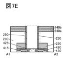
- 7A to 7F are cross-sectional views showing an example of a method for manufacturing a semiconductor device.
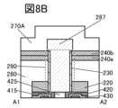
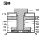
- 8A to 8F are cross-sectional views showing an example of a method for manufacturing a semiconductor device.
- 9A and 9B are cross-sectional views showing an example of a semiconductor device.
- 10A and 10B are cross-sectional views showing an example of a semiconductor device.
- 11A and 11B are cross-sectional views showing an example of a semiconductor device.
- 12A and 12B are cross-sectional views showing an example of a semiconductor device.
- 13A is a plan view illustrating an example of a semiconductor device
- FIG 13B is a cross-sectional view illustrating an example of the semiconductor device.
- FIG. 14A, 14B, 14C, and 14D are conceptual diagrams illustrating cross sections of an oxide semiconductor layer.
- FIG. 15 is a diagram illustrating the crystal structure of HfO 2 disclosed in Non-Patent Document 2.
- FIG. 16 is a block diagram illustrating a configuration example of a semiconductor device. 17A to 17E are diagrams for explaining examples of the circuit configuration of a memory cell. 18A and 18B are perspective views illustrating a configuration example of a semiconductor device.
- FIG. 19 is a cross-sectional view showing an example of a semiconductor device.
- FIG. 20 is a cross-sectional view showing an example of a semiconductor device.
- FIG. 21 is a block diagram illustrating the CPU. 22A and 22B are perspective views of a semiconductor device.
- 23A and 23B are perspective views of a semiconductor device.
- 24A and 24B are diagrams showing various storage devices by hierarchical level.
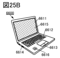
- 25A and 25B are diagrams showing an example of electronic equipment
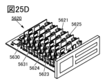
- FIGS. 25C to 25E are diagrams showing an example of a mainframe computer.
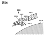
- FIG. 26 is a diagram showing an example of space equipment.
- FIG. 27 is a diagram illustrating an example of a storage system that can be applied to a data center.
- ordinal numbers “first” and “second” are used for convenience and do not limit the number of components or the order of the components (e.g., process order or stacking order).
- an ordinal number attached to a component in one place in this specification may not match an ordinal number attached to the same component in another place in this specification or in the claims.
- film and “layer” can be interchanged depending on the circumstances.
- the term “conductive layer” can be changed to the term “conductive film”.
- the term “insulating film” can be changed to the term “insulating layer”.
- the term “conductor” can be interchanged with the term “conductive layer” or the term “conductive film” depending on the circumstances.
- the term “insulator” can be interchanged with the term “insulating layer” or the term “insulating film” depending on the circumstances.
- oxide semiconductor can be interchanged with the term “oxide semiconductor layer” or the term “oxide semiconductor film” depending on the circumstances.
- parallel refers to a state in which two straight lines are arranged at an angle of -10 degrees or more and 10 degrees or less. Therefore, it also includes cases in which the angle is -5 degrees or more and 5 degrees or less.
- approximately parallel refers to a state in which two straight lines are arranged at an angle of -30 degrees or more and 30 degrees or less.
- Perfect refers to a state in which two straight lines are arranged at an angle of 80 degrees or more and 100 degrees or less. Therefore, it also includes cases in which the angle is 85 degrees or more and 95 degrees or less.
- approximately perpendicular refers to a state in which two straight lines are arranged at an angle of 60 degrees or more and 120 degrees or less.
- Openings include, for example, grooves, slits, and recesses. Also, the area in which an opening is formed may be referred to as an opening.
- drawings used in this specification show cases where the sidewalls of the insulator at the opening in the insulator are perpendicular or approximately perpendicular to the substrate surface or the surface on which the insulator is formed, but they may also be tapered.
- a tapered shape refers to a shape in which at least a portion of the side of the structure is inclined relative to the substrate surface or the surface on which the structure is to be formed.
- the angle between the inclined side and the substrate surface or the surface on which the structure is to be formed (hereinafter, sometimes referred to as the taper angle) is less than 90° in a region.
- the side of the structure and the substrate surface do not necessarily need to be completely flat, and may be approximately planar with a slight curvature, or approximately planar with minute irregularities.
- a reverse tapered shape refers to a shape with a side or top that protrudes in a direction parallel to the substrate more than the bottom.
- equal height refers to a configuration in which the heights from a reference surface (for example, a flat surface such as a substrate surface) are equal in cross-sectional view.
- a planarization process typically a chemical mechanical polishing (CMP) process
- CMP chemical mechanical polishing
- the surfaces treated in the CMP process have a configuration in which the heights from the reference surface are equal.
- the heights of multiple layers may differ depending on the processing device, processing method, or material of the processed surface during the CMP process. In this specification, this case is also treated as "equal height”.
- first layer and a second layer when there are two layers (here, a first layer and a second layer) with different heights relative to the reference surface, and the difference in height between the top surface of the first layer and the top surface of the second layer is 20 nm or less, this is also referred to as "equal height".
- side edges coincide means that at least a portion of the contours of the stacked layers overlap when viewed in a plane. For example, this includes cases where the upper and lower layers are processed using the same mask pattern, or where a portion of the mask pattern is the same. However, strictly speaking, the contours may not overlap, and the contour of the upper layer may be located inside the contour of the lower layer, or the contour of the upper layer may be located outside the contour of the lower layer, in which case it is also referred to as "side edges coincide”.
- the first film thickness and the second film thickness being the same means that the absolute value of the difference between the first film thickness and the second film thickness divided by the first film thickness is 0.1 or less. Alternatively, it means that the absolute value of the difference between the first film thickness and the second film thickness divided by the second film thickness is 0.1 or less.
- distance A and distance B are the same means that the absolute value of the difference between distance A and distance B divided by distance A is 0.1 or less. Alternatively, it means that the absolute value of the difference between distance A and distance B divided by distance B is 0.1 or less.
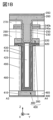
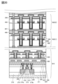
- FIGS. 1A to 2C are plan views and cross-sectional views of a semiconductor device including a transistor 200 and a capacitor 400.
- FIG. 2A is a plan view of the semiconductor device.
- FIG. 1A is a cross-sectional view of a portion indicated by a dashed line A1-A2 in FIG. 2A.
- FIG. 1B is a cross-sectional view of a portion indicated by a dashed line A3-A4 in FIG. 2A.
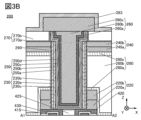
- FIG. 2B is a cross-sectional view of a portion of the transistor 200 in the XY plane in FIG.
- FIG. 2C is a cross-sectional view of a portion of the capacitor 400 in the XY plane in FIG. 2A. Note that some elements are omitted from the plan view of FIG. 1A for clarity.
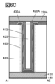
- FIGS. 3A and 3B are enlarged views of the transistor 200 shown in FIG. 1A.
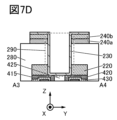
- FIG. 4 is an enlarged view of the capacitor 400 shown in FIG. 1B.
- FIG. 2D is a circuit diagram of the semiconductor device shown in FIGS. 1 and 2.
- arrows indicating the X-direction, Y-direction, and Z-direction may be used.
- the "X-direction” refers to the direction along the X-axis, and may not distinguish between the forward direction and the reverse direction unless otherwise specified. The same applies to the "Y-direction” and "Z-direction”.
- the X-direction, Y-direction, and Z-direction are directions that intersect with each other.
- the X-direction, Y-direction, and Z-direction are directions that are perpendicular to each other.
- one of the X-direction, Y-direction, and Z-direction may be called the "first direction” or “first direction”.
- the other may be called the “second direction” or “second direction”.
- the remaining one may be called the "third direction” or "third direction”.
- the semiconductor device shown in Figures 1A and 1B has an insulator 440 on a substrate (not shown), an insulator 485 and a conductor 410 on the insulator 440, an insulator 480 and a capacitor 400 on the insulator 485 and the conductor 410, a transistor 200 on the capacitor 400, an insulator 280 on the insulator 480, an insulator 270 on the insulator 280, and an insulator 283 on the transistor 200.
- the insulators 440, 485, 480, 280, and 270 function as interlayer insulating films.
- the insulator 440 also functions as a base insulator.
- the transistor 200 has a conductor 220 on the capacitor 400, a conductor 240 on the insulator 280, an oxide semiconductor 230 in contact with the conductor 220 and the conductor 240, an insulator 250 on the oxide semiconductor 230 and the insulator 270, and a conductor 260 on the insulator 250.
- the conductor 240 also has a conductor 240a and a conductor 240b on the conductor 240a.
- the capacitor 400 has a conductor 415 on the conductor 410, an insulator 430 on the conductor 415, and a conductor 420 on the insulator 430.
- An insulator 425 is provided on the conductor 420.
- the conductor 260 functions as a gate electrode
- the insulator 250 functions as a gate insulator
- the conductor 220 functions as one of the source electrode and the drain electrode
- the conductor 240 functions as the other of the source electrode and the drain electrode.
- the transistor 200 preferably uses a metal oxide (also called an oxide semiconductor) that functions as a semiconductor for the oxide semiconductor 230 including the channel formation region.
- a metal oxide also called an oxide semiconductor
- OS transistor a transistor using an oxide semiconductor in a channel formation region, such as the transistor 200, may be referred to as an OS transistor.
- insulator 280, conductor 240a, conductor 240b, and conductor 220 have openings 290 that reach insulator 425 and conductor 420.
- the bottom of opening 290 is the top surfaces of insulator 425 and conductor 420.
- the side walls of opening 290 are the side surfaces of insulator 280, conductor 240a, conductor 240b, and conductor 220.
- Opening 290 includes an opening in insulator 280, an opening in conductor 240a, an opening in conductor 240b, and an opening in conductor 220.
- the opening that the insulator 280 has in the area where it overlaps with the insulator 425 and the conductor 420 is part of the opening 290
- the opening that the conductor 240a has in the area where it overlaps with the insulator 425 and the conductor 420 is another part of the opening 290
- the opening that the conductor 240b has in the area where it overlaps with the insulator 425 and the conductor 420 is another part of the opening 290
- the opening that the conductor 220 has in the area where it overlaps with the insulator 425 and the conductor 420 is another part of the opening 290.
- At least some of the components of the transistor 200 are disposed in the opening 290.
- the oxide semiconductor 230, the insulator 250, and the conductor 260 are each disposed such that at least a portion of each of them is located in the opening 290.
- the portions of the oxide semiconductor 230, the insulator 250, and the conductor 260 that are arranged in the opening 290 are provided to reflect at least a part of the shape of the opening 290. That is, the oxide semiconductor 230 is provided in contact with the sidewall of the opening 290, the insulator 250 is provided to cover the oxide semiconductor 230, and the conductor 260 is provided to fill the recess of the insulator 250 that reflects the shape of the opening 290.
- the transistor 200 has a configuration in which one of the source electrode and drain electrode (here, conductor 220) is located on the bottom and the other of the source electrode and drain electrode (here, conductor 240) is located on the top, so that current flows in the vertical direction.
- a channel is formed along the side of the opening 290 of the insulator 280. Therefore, the transistor that is one embodiment of the present invention can be called a vertical channel transistor or a VFET (Vertical Field Effect Transistor).
- the conductor 420 functions as one of a pair of electrodes (sometimes called the upper electrode), the conductor 415 functions as the other of the pair of electrodes (sometimes called the lower electrode), and the insulator 430 functions as a dielectric.
- the capacitance element 400 constitutes a MIM (Metal-Insulator-Metal) capacitance.
- the insulator 480 has an opening 490 that reaches the conductor 410. At least a portion of each of the conductor 415, the insulator 430, the conductor 420, and the insulator 425 is disposed within the opening 490.
- the conductor 415, the insulator 430, and the conductor 420 are stacked along the shape of the opening 490.
- the capacitance element 400 having such a configuration can be called a trench type capacitance or trench capacitance.
- the insulator 425 is preferably provided so as to fill a recess that reflects the shape of the opening 490 of the conductor 420.
- the capacitive element 400 is configured such that the upper electrode and the lower electrode face each other across a dielectric not only on the bottom surface but also on the side surfaces of the opening 490, allowing the capacitance per unit area to be increased. Therefore, the deeper the opening 490, the greater the capacitance of the capacitive element 400 can be. Increasing the capacitance per unit area of the capacitive element 400 in this way can stabilize the read operation of the memory device. It can also promote miniaturization or high integration of memory devices.
- the transistor 200 is provided so as to overlap with the capacitor 400. Furthermore, the opening 290 in which part of the structure of the transistor 200 is provided has a region that overlaps with the opening 490 in which part of the structure of the capacitor 400 is provided.
- the conductor 260 overlaps with the insulator 425. It is also preferable that the bottom surface of the insulator 250 contacts the top surface of the insulator 425.
- the bottom surface of the conductor 220 contacts the top surface of the conductor 420. This allows electrical connection between one of the source electrode and drain electrode of the transistor 200 and the top electrode of the capacitance element 400.
- the transistor 200 and the capacitor 400 shown in this embodiment can be used as memory cells of a storage device (hereinafter, sometimes referred to as memory cell 450).
- a circuit diagram of the memory cell 450 is shown in FIG. 2D.
- one of the source and drain of the transistor 200 is connected to one electrode of the capacitor 400.
- the other of the source and drain of the transistor 200 is connected to a wiring BIL.
- the gate of the transistor 200 is connected to a wiring WOL.
- the other electrode of the capacitor 400 is connected to a wiring CAL.
- the wiring BIL corresponds to the conductor 240 (conductor 240a and conductor 240b), the wiring WOL corresponds to the conductor 260, and the wiring CAL corresponds to the conductor 410.
- the conductor 260 is provided extending in the Y direction, and the conductor 240 is provided extending in the X direction.
- the wiring BIL and the wiring WOL are provided intersecting each other.
- the wiring CAL (conductor 410) is provided extending in the X direction, but the present invention is not limited to this.
- the wiring CAL may be provided extending in the Y direction, or may be provided in a planar shape.
- the memory cell 450 reduces the area occupied by the transistor 200 and the capacitor 400 by overlapping them.
- the transistor and the capacitor are overlapped in this way, the transistor and the capacitor are arranged in an overlapping manner, which may cause parasitic capacitance and reduce the operating speed of the memory element. Therefore, in this embodiment, an insulator 425 is provided between the conductor 260 and the conductor 420, increasing the distance between the conductor 260 and the conductor 420 in most of the area where the conductors 260 and 420 overlap. This makes it possible to reduce the parasitic capacitance between the gate of the transistor 200 and the upper electrode of the capacitor 400. Therefore, the operating speed of the memory cell 450 consisting of the transistor 200 and the capacitor 400 can be improved.
- the oxide semiconductor 230 included in the transistor 200 is formed along a sidewall of the opening 290.
- the oxide semiconductor 230 is in contact with the side surface of the conductor 240a on the opening 290 side, the side surface of the conductor 240b on the opening 290 side, the side surface of the insulator 280 on the opening 290 side, and the side surface of the conductor 220 on the opening 290 side.
- the oxide semiconductor 230 is not formed so as to cover the bottom surface of the opening 290, and has a cylindrical shape with an opening in the center. It can be said that at least a part of the bottom surface of the oxide semiconductor 230 is removed in the opening 290.
- the oxide semiconductor 230 is formed in a sidewall shape with respect to the opening 290. Therefore, the insulator 250 is disposed in contact with the inner side surface of the oxide semiconductor 230, and at the bottom surface of the opening 290, the insulator 250 is in contact with the upper surface of the conductor 420 and the upper surface of the insulator 425. Furthermore, the oxide semiconductor 230 is not formed to cover the conductor 240b, and is not in contact with the upper surface of the conductor 240b. Here, the upper end of the oxide semiconductor 230 may coincide or roughly coincide with the upper surface of the conductor 240b.
- a parasitic capacitance is formed between the oxide semiconductor at the bottom of the opening 290 and the conductor 420.
- a parasitic capacitance is also formed between the oxide semiconductor at the bottom of the opening 290 and the conductor 260.
- the oxide semiconductor 230 is not formed at the bottom of the opening 290. Therefore, the parasitic capacitance between the oxide semiconductor 230 and the conductor 420, and the parasitic capacitance between the oxide semiconductor 230 and the conductor 260 can be suppressed. This makes it possible to form a transistor with good frequency characteristics and improve the operating speed of the semiconductor device.
- the oxide semiconductor 230 has a source region and a drain region formed on either side of the channel formation region.
- One of the source region and the drain region includes at least a part of the region of the oxide semiconductor 230 that is in contact with the conductor 240.
- the other of the source region and the drain region includes at least a part of the region of the oxide semiconductor 230 that is in contact with the conductor 220.
- the channel formation region of the transistor 200 is located in the region of the oxide semiconductor 230 between the conductor 220 and the conductor 240. It can also be said that the channel formation region of the transistor 200 is located in the region of the oxide semiconductor 230 that is in contact with the insulator 280 or in a region nearby the region.
- the channel length of the transistor 200 is the distance between the source region and the drain region. In other words, it can be said that the channel length of the transistor 200 is determined by the thickness of the insulator 280 on the conductor 220.
- the channel length L of the transistor 200 is indicated by a dashed double-headed arrow. In a cross-sectional view, the channel length L is the distance between the end of the region where the oxide semiconductor 230 and the conductor 220 contact each other and the end of the region where the oxide semiconductor 230 and the conductor 240 contact each other. It can also be said that the channel length L corresponds to the distance between the upper surface of the conductor 220 and the lower surface of the conductor 240a in a cross-sectional view.
- FIG. 2B A cross-sectional view of the XY plane in the region between the conductor 220 and the conductor 240 is shown in FIG. 2B.
- the oxide semiconductor 230, the insulator 250, and the conductor 260 are arranged concentrically inside the opening 290 of the insulator 280. Therefore, the side surface of the conductor 260 arranged in the center faces the side surface of the oxide semiconductor 230 via the insulator 250. In other words, in the region between the conductor 220 and the conductor 240, the entire circumference of the oxide semiconductor 230 becomes the channel formation region.
- the conductor 220 is not formed with the opening 290 penetrating it and the upper surface of the conductor 220 is formed with a flat shape, the insulator 250 is formed on the conductor 220, and the lower surface of the conductor 260 is higher than the upper surface of the conductor 220.
- the contact between the oxide semiconductor 230 and the conductor 220 becomes bottom contact that is mainly performed on the lower surface of the oxide semiconductor 230.
- the concentric structure of the oxide semiconductor 230, the insulator 250, and the conductor 260 shown in FIG. 2B is no longer formed.
- an offset region is formed in the oxide semiconductor 230 in the vicinity of the conductor 220, which may cause a decrease in the electrical characteristics of the transistor, such as the on-current, subthreshold swing value (hereinafter sometimes referred to as S value), field effect mobility, and frequency characteristics.
- S value the on-current, subthreshold swing value
- the height of the bottom surface of the conductor 260 is lower than the height of the top surface of the conductor 220 in the region that does not overlap with the opening 290.
- the contact between the oxide semiconductor 230 and the conductor 220 is a side contact that is mainly made on the side surface of the oxide semiconductor 230.
- the oxide semiconductor 230, the insulator 250, and the conductor 260 can be arranged concentrically even in the region near the conductor 220. That is, in the region near the conductor 220, the side surfaces of the conductor 260 and the oxide semiconductor 230 can be arranged to face each other through the insulator 250. Therefore, even in the vicinity of the conductor 220, the electric field of the conductor 260 functioning as a gate electrode can be sufficiently applied to the oxide semiconductor 230. This makes it possible to suppress the formation of an offset region in the oxide semiconductor 230 near the conductor 220. In this way, the electrical characteristics of the transistor 200, such as the on-current, the S value, the field effect mobility, and the frequency characteristics, can be improved.
- the channel length is limited by the exposure limit of lithography, making further miniaturization difficult.
- the channel length can be set by the film thickness of the insulator 280 on the conductor 220. Therefore, the channel length L of the transistor 200 can be, for example, 1 ⁇ m or less, 500 nm or less, 100 nm or less, 60 nm or less, 50 nm or less, 40 nm or less, 30 nm or less, 20 nm or less, or 10 nm or less, and 0.1 nm or more, 1 nm or more, or 5 nm or more.
- the channel length L a very fine structure below the exposure limit of lithography, the on-current, S value, frequency characteristics, and the like of the transistor 200 can be improved. Also, for example, by increasing the channel length L, DIBL (Drain Induced Barrier Lowering) can be suppressed in the transistor 200, and electrical characteristics can be improved.
- DIBL Drain Induced Barrier Lowering
- a channel formation region, a source region, and a drain region can be formed in the opening 290.
- the channel length L can be made larger than the width in the X direction and the width in the Y direction of the transistor 200. This allows the semiconductor device to be highly integrated.
- the semiconductor device of one embodiment of the present invention is used for a memory device, the memory capacity per unit area can be increased.
- the channel width of the transistor 200 is determined by the maximum width of the opening 290 (the maximum diameter if the opening 290 is circular in plan view).
- the maximum width D of the opening 290 is indicated by a double-headed arrow with two dots and dashes.
- the channel width W of the transistor 200 is indicated by a double-headed arrow with one dot and dashes.
- the maximum width D of the opening 290 is limited by the exposure limit of the lithography.
- the maximum width D of the opening 290 is set by the film thickness of each of the oxide semiconductor 230, the insulator 250, and the conductor 260 provided in the opening 290.
- the maximum width D of the opening 290 is, for example, 5 nm or more, 10 nm or more, or 20 nm or more, and is preferably 100 nm or less, 60 nm or less, 50 nm or less, 40 nm or less, or 30 nm or less.
- the maximum width D of the opening 290 corresponds to the diameter of the opening 290, and the channel width W can be calculated as "D x ⁇ ".
- the oxide semiconductor 230, the insulator 250, and the conductor 260 are arranged concentrically. This makes the distance between the conductor 260 and the oxide semiconductor 230 roughly uniform, so that a gate electric field can be applied roughly uniformly to the oxide semiconductor 230.
- the opening 290 is circular in plan view, but the present invention is not limited to this.
- the opening 290 may be approximately circular such as an ellipse, polygonal such as a rectangle, or polygonal such as a rectangle with rounded corners in plan view.
- the maximum width of the opening 290 can be calculated appropriately according to the shape of the top of the opening 290. For example, if the opening is rectangular in plan view, the maximum width of the opening 290 can be considered to be the length of the diagonal line at the top of the opening 290.
- the sidewalls of the opening 290 are perpendicular or approximately perpendicular to the upper surface of the insulator 440. With such a configuration, it is possible to miniaturize or highly integrate the semiconductor device.
- the opening 290 is provided so that the sidewall of the opening 290 is perpendicular to the top surface of the conductor 220, but the present invention is not limited to this.
- the sidewall of the opening 290 may not be strictly perpendicular and may have a tapered shape.
- the taper angle formed by the side surface of the insulator 280, which is part of the sidewall of the opening 290, and the top surface of the conductor 220 (which may be the top surface of the insulator 480 or the top surface of the insulator 440) is preferably 90 degrees or close to 90 degrees.
- the taper angle is preferably 75 degrees or more and 90 degrees or less.
- the taper angle may be less than 75 degrees, less than 70 degrees, less than 65 degrees, or less than 60 degrees.
- the metal oxides described in the section [Metal Oxides] below can be used in a single layer or a multilayer structure.
- the composition close thereto includes a range of ⁇ 30% of the desired atomic ratio. It is also preferable to use one or more of gallium, aluminum, and tin as the element M.
- the oxide semiconductor 230 may be configured not to include the element M.
- the metal oxide used as the oxide semiconductor 230 may be an In-Zn oxide.
- indium oxide may be used as the oxide semiconductor 230.
- the oxide semiconductor 230 may also be configured to include a trace amount of the element M.
- the composition of the metal oxide used in the oxide semiconductor 230 can be analyzed using, for example, energy dispersive X-ray spectroscopy (EDX), X-ray photoelectron spectroscopy (XPS), inductively coupled plasma mass spectrometry (ICP-MS), or inductively coupled plasma-atomic emission spectrometry (ICP-AES).
- EDX energy dispersive X-ray spectroscopy
- XPS X-ray photoelectron spectroscopy
- ICP-MS inductively coupled plasma mass spectrometry
- ICP-AES inductively coupled plasma-atomic emission spectrometry
- a combination of these techniques may be used for the analysis.
- the actual content may differ from the content obtained by analysis due to the influence of analytical accuracy. For example, if the content of element M is low, the content of element M obtained by analysis may be lower than the actual content.
- the metal oxide can be formed preferably by sputtering or atomic layer deposition (ALD).
- ALD atomic layer deposition
- the composition of the formed metal oxide may differ from the composition of the sputtering target.
- the zinc content in the formed metal oxide may decrease to about 50% compared to the sputtering target.
- Examples of the ALD method include the Thermal ALD method, in which the reaction between the precursor and reactant is carried out using only thermal energy, and the Plasma Enhanced ALD (PEALD) method, in which a plasma-excited reactant is used.
- Thermal ALD method in which the reaction between the precursor and reactant is carried out using only thermal energy
- PEALD Plasma Enhanced ALD
- the ALD method can deposit atoms one layer at a time, and therefore has the following advantages: extremely thin films can be formed; films can be formed on structures with high aspect ratios or surfaces with large steps; films can be formed with few defects such as pinholes; films can be formed with excellent coverage; and films can be formed at low temperatures.
- the PEALD method may be preferable because it uses plasma, which allows films to be formed at lower temperatures.
- some precursors used in the ALD method contain elements such as carbon or chlorine.
- films formed by the ALD method may contain more elements such as carbon or chlorine than films formed by other film formation methods. Note that the quantification of these elements can be performed using XPS or SIMS.
- the metal oxide film formation method of one embodiment of the present invention uses the ALD method, but adopts one or both of the conditions of a high substrate temperature during film formation and the implementation of an impurity removal process, so that the amount of carbon and chlorine contained in the film may be smaller than when the ALD method is used without applying these.
- the ALD method is a film formation method in which a film is formed by a reaction on the surface of a workpiece, unlike a film formation method in which particles released from a target are deposited. Therefore, it is a film formation method that is not easily affected by the shape of the workpiece and has good step coverage.
- the ALD method has excellent step coverage and excellent thickness uniformity, making it suitable for coating the surface of an opening with a high aspect ratio.
- the ALD method since the ALD method has a relatively slow film formation speed, it may be preferable to use it in combination with other film formation methods such as a sputtering method or a CVD method, which have a fast film formation speed.
- the metal oxide has a layered structure of a first metal oxide and a second metal oxide
- a method of forming a film of the first metal oxide using a sputtering method and forming a film of the second metal oxide on the first metal oxide using an ALD method can be mentioned.
- the first metal oxide has a crystal part
- the second metal oxide may grow as a crystal with the crystal part as a nucleus.
- the ALD method can control the composition of the resulting film by the amount of raw material gas introduced.
- the ALD method can form a film of any composition by adjusting the amount of raw material gas introduced, the number of times it is introduced (also called the number of pulses), the time required for one pulse (also called the pulse time), and the like.
- the ALD method can form a film whose composition changes continuously by changing the raw material gas while forming the film.
- the time required for film formation can be shortened compared to forming a film using multiple film formation chambers because no time is required for transportation and pressure adjustment. Therefore, the productivity of semiconductor devices can be increased in some cases.
- the method for forming the oxide semiconductor film that becomes the oxide semiconductor 230 is not particularly limited.
- the oxide semiconductor film may be formed using a CVD method, an MBE method, a PLD method, or the like.
- the crystallinity of the semiconductor material used for the oxide semiconductor 230 is not particularly limited, and any of an amorphous semiconductor (a semiconductor having an amorphous structure), a single crystal semiconductor (a semiconductor having a single crystal structure), or a semiconductor having crystallinity other than single crystal (a microcrystalline semiconductor, a polycrystalline semiconductor, or a semiconductor having a crystalline region in part) may be used.
- a single crystal semiconductor or a semiconductor having crystallinity is preferable because it can suppress deterioration of the transistor characteristics.
- the oxide semiconductor 230 preferably has a metal oxide layer having crystallinity.
- a metal oxide having crystallinity examples include a CAAC (c-axis aligned crystal) structure, a polycrystalline (Poly-crystal) structure, and a nanocrystalline (nc: nano-crystal) structure.
- CAAC c-axis aligned crystal
- Poly-crystal polycrystalline
- nc nanocrystalline
- the CAAC structure is a crystal structure in which multiple microcrystals (typically multiple IGZO microcrystals) have a c-axis orientation and are connected without being oriented in the a-b plane.
- the OS film having a CAAC structure can also be said to have a structure having layered crystal parts.
- the polycrystalline structure has grain boundaries.
- tiny gaps also called nanocracks or microcracks
- tiny spaces also called nanospaces or microspaces
- the electrical resistance of the oxide semiconductor layer increases. This is because the electrical resistance of the tiny gaps or tiny spaces is very high, for example, infinite.
- the contact resistance between the oxide semiconductor layer and one or both of the source electrode and the drain electrode increases. This adversely affects the initial characteristics or reliability of the transistor.
- the CAAC structure has fewer grain boundaries in the a-b plane than the polycrystalline structure, and therefore can realize a highly reliable semiconductor device.
- the crystallinity of the oxide semiconductor 230 can be analyzed, for example, by X-ray diffraction (XRD), a transmission electron microscope (TEM), or electron diffraction (ED). Alternatively, the analysis may be performed by combining a plurality of these techniques.
- XRD X-ray diffraction
- TEM transmission electron microscope
- ED electron diffraction
- the oxide semiconductor 230 may have a laminated structure of multiple oxide layers with different chemical compositions. For example, it may have a structure in which multiple types of metal oxides selected from those described in the [Metal Oxide] section below are appropriately laminated.
- the oxide semiconductor 230 can have a stacked structure of two or more metal oxide layers with different crystallinity.
- the two or more metal oxide layers may have different compositions or may have the same or approximately the same composition.
- the oxide semiconductor 230 may have a two-layer structure of an oxide semiconductor 230a and an oxide semiconductor 230b inside the oxide semiconductor 230a.
- the two-layer structure can be formed by forming a metal oxide film to be the oxide semiconductor 230a and then forming a metal oxide film to be the oxide semiconductor 230b thereon.
- the oxide semiconductor 230b can have a structure having a region with higher crystallinity than the oxide semiconductor 230a.
- the oxide semiconductor 230b can have a structure having a region with lower crystallinity than the oxide semiconductor 230a. Note that when the oxide semiconductor 230b has a region with lower crystallinity than the oxide semiconductor 230a, the oxide semiconductor 230b is formed and then subjected to heat treatment (also referred to as crystallization treatment) to increase the crystallinity of the oxide semiconductor 230b.
- heat treatment also referred to as crystallization treatment
- the oxide semiconductor 230b by forming the oxide semiconductor 230b on the oxide semiconductor 230a having high crystallinity, it is also easy to improve the crystallinity of the oxide semiconductor 230b. This makes it possible to improve the crystallinity of the entire oxide semiconductor 230, which is preferable.
- gallium, aluminum, or tin as the element M.
- two layers of IGZO having different compositions may be stacked.
- a laminated structure of any one selected from indium oxide, indium gallium oxide, and IGZO and any one selected from IAZO, IAGZO, and ITZO (registered trademark) may be used.
- the oxide semiconductor 230 may also have a stacked structure of three or more layers. As shown in FIG. 3B, the oxide semiconductor 230 disposed inside the opening 290 may have a three-layer structure having, for example, an oxide semiconductor 230c in contact with the sidewall of the opening 290, an oxide semiconductor 230a in contact with the side surface of the oxide semiconductor 230c on the central side of the opening 290, and an oxide semiconductor 230b in contact with the side surface of the oxide semiconductor 230a on the central side of the opening 290.
- the above-mentioned configuration can be applied to the oxide semiconductor 230a and the oxide semiconductor 230b.
- the oxide semiconductor 230c located on the outer side of the oxide semiconductor 230a can have the same configuration as that applicable to the oxide semiconductor 230b.
- the oxide semiconductor 230b and the oxide semiconductor 230c preferably have a larger band gap than the oxide semiconductor 230a.
- the oxide semiconductor 230a is sandwiched between the oxide semiconductor 230b and the oxide semiconductor 230c, which have a larger band gap, and the oxide semiconductor 230a mainly functions as a current path (channel).
- sandwiching the oxide semiconductor 230a between the oxide semiconductor 230b and the oxide semiconductor 230c it is possible to reduce the trap level at the interface of the oxide semiconductor 230a and its vicinity.
- a buried channel type transistor in which the channel is away from the insulating layer interface can be realized, and the field effect mobility can be increased.
- the influence of the interface state that may be formed on the back channel side is reduced, and the light deterioration of the transistor (for example, negative bias light deterioration) can be suppressed, and the reliability of the transistor can be improved.
- the thickness of the oxide semiconductor 230 is preferably 3 nm or more and 200 nm or less, more preferably 3 nm or more and 100 nm or less, more preferably 5 nm or more and 100 nm or less, more preferably 10 nm or more and 100 nm or less, more preferably 10 nm or more and 70 nm or less, more preferably 15 nm or more and 70 nm or less, more preferably 15 nm or more and 50 nm or less, and more preferably 20 nm or more and 50 nm or less.
- the thickness of the oxide semiconductor 230 is preferably 1 nm or more, 3 nm or more, or 5 nm or more, and 20 nm or less, 15 nm or less, 12 nm or less, or 10 nm or less.
- the oxide semiconductor layer when forming the oxide semiconductor layer, it is preferable to use two types of film formation methods, a sputtering method and an ALD method. For example, if a first oxide semiconductor layer having a CAAC structure is formed by a sputtering method and then a second oxide semiconductor layer having a lower crystallinity than the CAAC structure is formed by an ALD method, it is expected that the atomic layer of the second oxide semiconductor layer fills or repairs the gaps in the atomic-level crystal parts of the CAAC structure of the first oxide semiconductor layer. In addition, it is preferable to perform heat treatment (for example, 100° C. or more and 500° C. or less, preferably 200° C. or more and 450° C. or less, more preferably 300° C.
- heat treatment for example, 100° C. or more and 500° C. or less, preferably 200° C. or more and 450° C. or less, more preferably 300° C.
- the second oxide semiconductor layer (in other words, each crystal molecule formed by the ALD method) repairs the gaps in the atomic-level crystal parts of the CAAC structure of the first oxide semiconductor layer by the heat treatment.
- an oxide semiconductor layer formed using the above two types of film formation methods may be called a hybrid OS.
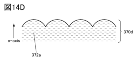
- Figures 14A, 14B, 14C, and 14D are conceptual diagrams for explaining a cross section of an oxide semiconductor layer having a CAAC structure.
- the c-axis is indicated by an arrow in each figure.
- the oxide semiconductor layer 370a shown in FIG. 14A has a region 372a and a region 372b located between the regions 372a.
- the region 372a corresponds to a region of a CAAC structure (i.e., a structure having layered crystal portions), and the region 372b corresponds to a region between the CAAC structures.
- the CAAC structure has fewer grain boundaries in the a-b plane than the polycrystalline structure. Thus, even in the oxide semiconductor layer 370a having a CAAC structure, there may be a minute gap or minute space between the crystal portions (region 372b in FIG. 14A).
- an oxide semiconductor layer having a CAAC structure is formed by sputtering as the first oxide semiconductor layer, and then an oxide semiconductor layer having a microcrystalline structure or an amorphous structure, which has lower crystallinity than the CAAC structure, is formed by ALD as the second oxide semiconductor layer.
- an oxide semiconductor layer having a region 372a is formed by sputtering as a first oxide semiconductor layer, and then an oxide semiconductor layer having a region 372c with lower crystallinity than the CAAC structure is formed by ALD as a second oxide semiconductor layer.
- the oxide semiconductor layer 370b has regions 372a and 372c. Since the ALD method can deposit atoms one layer at a time, the second oxide semiconductor layer can be formed to fill region 372b.
- the oxide semiconductor layer 370c has a region 372a and a region 372c.
- the 14C is a region having higher crystallinity or a higher density of crystal parts than the region 372a shown in FIG. 14B.
- the crystallinity of either or both of the regions 372a and 372c can be increased.
- the region 372c has, for example, a crystal part that has the same crystal structure as the crystal part of the region 372a.
- the region 372c has, for example, a crystal part that is connected to the crystal part of the region 372a.
- the oxide semiconductor layer 370d has a region 372a.
- the region 372a has improved crystallinity compared to the region 372a shown in FIG. 14B and FIG. 14C, and the boundary between the region 372a and the region 372c disappears, or the boundary between the region 372a and the region 372c is no longer observed. Therefore, the entire oxide semiconductor layer 370d has a CAAC structure.
- FIG. 14D when the entire oxide semiconductor layer 370d has a CAAC structure, a highly reliable semiconductor device can be realized. The presence or absence of the boundary between the region 372a and the region 372c can be confirmed, for example, by using a cross-sectional TEM, a cross-sectional STEM, or the like.
- the minute gap or the minute space in the first oxide semiconductor layer can be filled by forming a second oxide semiconductor layer on the first oxide semiconductor layer or by forming a second oxide semiconductor layer and performing heat treatment.
- a dense oxide semiconductor layer with increased crystallinity can be obtained.
- the dense oxide semiconductor layer with increased crystallinity is used for the channel formation region of a transistor, it is expected that an increase in the electrical resistance of the oxide semiconductor layer can be suppressed or the initial characteristics (particularly the on-current) of the transistor can be improved, making the transistor suitable for high-speed driving.
- the oxide semiconductor layer is formed by both the sputtering method and the ALD method, if the thickness of the oxide semiconductor layer formed by the ALD method is thin, the oxide semiconductor layer can be regarded as a single-layer structure, not a stacked structure of the oxide semiconductor layer formed by the sputtering method and the oxide semiconductor layer formed by the ALD method.
- the oxide semiconductor layer formed by the ALD method when the thickness of the oxide semiconductor layer formed by the ALD method is more than 0 nm and less than 3 nm, preferably more than 0 nm and less than 2 nm, and more preferably more than 0 nm and less than 1 nm, the oxide semiconductor layer formed by the two film formation methods, the sputtering method and the ALD method, can be regarded as a single-layer structure.
- the oxide semiconductor layer formed by the ALD method exceeds 3 nm, the oxide semiconductor layer formed by the sputtering method and the oxide semiconductor layer formed by the ALD method can be regarded as a stacked structure, a multilayer structure, or a multiple structure.
- the compositions are different from each other.
- the metal oxide film formed using the sputtering method has a composition suitable for forming a CAAC structure.
- the metal oxide film formed using the ALD method has a composition with a higher amount of indium than the metal oxide film formed using the sputtering method.
- the oxide semiconductor 230c by the ALD method.
- the vicinity of the surface on which the oxide semiconductor 230a is to be formed is prevented from being alloyed, and the crystallinity of the oxide semiconductor 230a can be further improved.
- the oxide semiconductor layer formed using the above two types of film formation methods can be considered to have a structure in which the gaps in the crystal parts of the CAAC structure are filled with atomic layers formed by the ALD method.
- This structure can be analyzed by analytical methods such as cross-sectional SEM, cross-sectional STEM, cross-sectional TEM, SIMS, and EDX.
- an oxide semiconductor layer having a CAAC structure formed using the above-mentioned two types of film formation methods may have a higher dielectric constant, film density, and film hardness than an oxide semiconductor layer having a CAAC structure formed using one type of film formation method.
- a transistor having excellent characteristics for example, a transistor with a large on-current, a transistor with high field-effect mobility, a transistor with a small S value, a transistor with high frequency characteristics (also called f characteristics), a highly reliable transistor, etc.
- the hydrogen concentration in the channel formation region of an oxide semiconductor measured by secondary ion mass spectrometry is preferably less than 1 ⁇ 10 20 atoms/cm 3 , more preferably less than 5 ⁇ 10 19 atoms/cm 3, still more preferably less than 1 ⁇ 10 19 atoms/cm 3, still more preferably less than 5 ⁇ 10 18 atoms/cm 3 , still more preferably less than 1 ⁇ 10 18 atoms/cm 3 , and still more preferably less than 1 ⁇ 10 17 atoms/cm 3 .
- the insulator 440 provided under the capacitor 400 and the insulator 283 provided over the transistor 200 use a barrier insulator against hydrogen.
- the insulator 440 and the insulator 283 can be provided to sandwich the memory cell 450.
- the insulator 440 and the insulator 283 provided on the outside of the transistor 200 including the oxide semiconductor 230 have a barrier property against hydrogen, so that the diffusion of hydrogen into the oxide semiconductor 230 can be suppressed.
- a barrier insulator refers to an insulator having barrier properties.
- the barrier properties refer to a property that a corresponding substance is difficult to diffuse (also referred to as a property that a corresponding substance is difficult to permeate, a property that the permeability of a corresponding substance is low, or a function of suppressing the diffusion of a corresponding substance).
- hydrogen refers to at least one of, for example, a hydrogen atom, a hydrogen molecule, and a substance bonded to hydrogen such as a water molecule and OH ⁇ .
- impurities when impurities are described as a corresponding substance, they refer to impurities in a channel formation region or a semiconductor layer unless otherwise specified, and refer to at least one of, for example, a hydrogen atom, a hydrogen molecule, a water molecule, a nitrogen atom, a nitrogen molecule, a nitrogen oxide molecule (N 2 O, NO, NO 2 , etc.), a copper atom, etc.
- oxygen when oxygen is described as a corresponding substance, it refers to at least one of, for example, an oxygen atom, an oxygen molecule, etc.
- Barrier insulators against hydrogen include aluminum oxide, magnesium oxide, hafnium oxide, gallium oxide, silicon nitride, and silicon oxide-nitride.
- the insulator 440 and the insulator 283 contain silicon and nitrogen.
- Silicon nitride which can be used as insulator 440 and insulator 283, has barrier properties against hydrogen if the film thickness is, for example, 2 nm or more.
- the silicon nitride film thickness is preferably 3 nm or more, and more preferably 5 nm or more.
- Silicon nitride has barrier properties against oxygen if the film thickness is, for example, 1 nm or more.
- the silicon nitride film thickness is preferably 2 nm or more. In other words, silicon nitride formed to a film thickness that has barrier properties against hydrogen also has barrier properties against oxygen.
- an insulator 480b having a function of trapping or fixing hydrogen is preferably used for the upper part of the insulator 480.
- the hydrogen concentration in the oxide semiconductor 230 located inside the insulator 440 and the insulator 283 can be reduced.
- hydrogen in the oxide semiconductor 230 is trapped or fixed by the insulator 480b, so that the hydrogen concentration in the insulator 480b is high.
- the hydrogen concentration of the insulator 480b obtained by SIMS may be 1 ⁇ 10 19 atoms/cm 3 or more or 1 ⁇ 10 20 atoms/cm 3 or more.
- the hydrogen concentration of at least a part of the insulator 480b is higher than the hydrogen concentration of the oxide semiconductor 230.
- the oxide semiconductor 230 has a region in which the hydrogen concentration is lower than the hydrogen concentration of the insulator 480b.
- the ability to capture or adhere to the corresponding substance can also be said to have the property of making the corresponding substance less likely to diffuse. Therefore, the ability to capture or adhere to the corresponding substance can be rephrased as barrier properties.
- a metal oxide containing hafnium or the like e.g., hafnium oxide, etc.
- the above metal oxide preferably has oxygen atoms with dangling bonds.
- Such metal oxides may have the property of capturing or fixing hydrogen with dangling bonds.
- the above metal oxide preferably has an amorphous structure. This is because in metal oxides with an amorphous structure, some oxygen atoms have dangling bonds.
- the above metal oxide preferably has an amorphous structure, but crystalline regions may be formed in some parts. Furthermore, the above metal oxide may have crystal grain boundaries in some parts.
- hafnium silicate an oxide containing hafnium and silicon (hereinafter, sometimes referred to as hafnium silicate) tends to have an amorphous structure. Therefore, hafnium silicate has the property of capturing or adhering hydrogen, making it suitable as insulator 480b. In this case, insulator 480b contains hafnium, silicon, and oxygen.
- oxides containing hafnium are listed as insulators having the function of capturing or fixing hydrogen, but the present invention is not limited to this.
- oxides containing magnesium, oxides containing aluminum, oxides containing aluminum and hafnium (hafnium aluminate), etc. may be listed.
- the above metal oxides may further contain oxides containing zirconium.
- oxides containing hafnium and zirconium, etc. are listed.
- it is preferable that these metal oxides have silicon added and have an amorphous structure.
- the insulator 280 is provided to cover the conductor 220, the conductor 420, and the insulator 430, and is in contact with the side surface of the oxide semiconductor 230 and the bottom surface of the conductor 240 (see Figures 1A and 1B).
- the insulator 280 is preferably formed using a material with a low relative dielectric constant. This allows the insulator 280 to function as an interlayer insulating film, thereby reducing the parasitic capacitance between the conductor 240 and the conductor 220. This allows the frequency characteristics of the transistor 200 to be improved.
- the insulator 280 a single layer or a stack of insulators containing a material with a low dielectric constant, as described in the [Insulator] section below, can be used. Specifically, silicon oxide or silicon oxynitride can be used as the insulator 280. Furthermore, it is preferable that the concentration of impurities such as water and hydrogen in the insulator 280 is reduced. This can suppress the intrusion of impurities such as water and hydrogen into the channel formation region of the oxide semiconductor 230.
- an insulator containing oxygen for the insulator 280.
- oxygen can be supplied to the oxide semiconductor 230 in contact with the insulator 280, making it easier to reduce oxygen vacancies.
- oxygen can be supplied to the oxide semiconductor 230.
- oxygen vacancies and VOH in the channel formation region of the oxide semiconductor 230 can be reduced, and a transistor with favorable electrical characteristics and high reliability can be obtained.
- the amount of released oxygen molecules from the insulator 280b is preferably equal to or greater than 1.0 ⁇ 10 14 molecules/cm 2 and less than 1.0 ⁇ 10 15 molecules/cm 2.
- the amount of released oxygen molecules can be measured by thermal desorption spectrometry.
- the channel length of the transistor 200 when the channel length of the transistor 200 is short, the influence of oxygen vacancies in the channel formation region and VOH on the electrical characteristics and reliability is particularly large. Therefore, by sufficiently reducing the hydrogen concentration in the oxide semiconductor 230 and then optimizing the amount of oxygen supplied to the oxide semiconductor 230, a transistor with a short channel length having favorable electrical characteristics and high reliability can be realized.
- the insulator 280 is preferably formed by a deposition method such as a sputtering method or a plasma enhanced chemical vapor deposition (PECVD) method.
- a deposition method such as a sputtering method or a plasma enhanced chemical vapor deposition (PECVD) method.
- PECVD plasma enhanced chemical vapor deposition
- oxygen supplied to the oxide semiconductor 230 for example, after forming the insulator 280, a heat treatment in an oxygen-containing atmosphere or a plasma treatment in an oxygen-containing atmosphere may be performed.
- oxygen may be supplied by forming an oxide film in an oxygen atmosphere on the upper surface of the insulator 280 by a sputtering method. The oxide film may then be removed. By performing such a treatment, oxygen can be supplied to the insulator 280, and the amount of oxygen supplied to the oxide semiconductor 230 can be increased.
- the insulator 280 can also be configured to use a barrier insulator against hydrogen.
- silicon nitride can be used for the insulator 280. With such a configuration, the diffusion of hydrogen into the oxide semiconductor 230 can be suppressed. Furthermore, it is preferable that the concentration of impurities such as water and hydrogen in the insulator 280 is reduced. This can suppress the intrusion of impurities such as water and hydrogen into the channel formation region of the oxide semiconductor 230.
- the insulator 280 is illustrated as having a single-layer structure, but is not limited thereto and may have a laminated structure.
- the insulator 280 may have a two-layer structure, with the height of the top surface of the first layer of insulator being the same as the height of the top surface of the conductor 220, and the second layer of insulator being provided on top of the first layer of insulator.
- the insulator 280 may have a layered structure of an insulator 280a, an insulator 280b on the insulator 280a, and an insulator 280c on the insulator 280b.
- Insulator 280a contacts the top surface of insulator 480, the side surface of insulator 430, the side surface of conductor 420, and the top and side surfaces of conductor 220.
- Insulator 280b contacts the top surface of insulator 280a and the bottom surface of insulator 280c.
- Insulator 280c contacts the bottom surface of conductor 240.
- an insulating material applicable to the insulator 280 described above may be used. Specifically, silicon oxide or silicon oxynitride may be used as the insulator 280b. In addition, it is preferable that the concentration of impurities such as water and hydrogen in the insulator 280b is reduced.
- insulator 280b When an insulator containing oxygen is used as insulator 280b, it is preferable to use a barrier insulator against oxygen as insulator 280a and insulator 280c, as described below in the section [Insulator].
- insulator 280a between insulator 280b and conductor 220 and conductor 420, excessive oxidation of conductor 220 and conductor 420, which would increase the resistance of conductor 220 and conductor 420, can be suppressed.
- insulator 280c between insulator 280b and conductor 240, excessive oxidation of conductor 240, which would increase the resistance of conductor 240, can be suppressed.
- the insulators 280a and 280c may each be a barrier insulator against hydrogen. This allows the insulator 280b to be sandwiched between the barrier insulators against hydrogen. This makes it possible to suppress the diffusion of hydrogen from below the insulator 280a or above the insulator 280c to the insulator 280b.
- the silicon nitride film and the silicon nitride oxide film each have the characteristics of releasing little impurities (e.g., water and hydrogen) from themselves and being difficult for oxygen and hydrogen to permeate, and therefore can be suitably used for the insulators 280a and 280c. Note that the insulators 280a and 280c may be made of the same material or different materials.
- an insulator having a function of capturing or fixing hydrogen may be used for one or both of the insulators 280a and 280c. With such a configuration, it is possible to suppress the diffusion of hydrogen from below the insulator 280a or above the insulator 280c to the insulator 280b, and further to capture or fix the hydrogen contained in the insulator 280b. Thus, it is possible to reduce the hydrogen concentration in the oxide semiconductor 230 and its vicinity.
- the insulator 280a magnesium oxide, aluminum oxide, hafnium oxide, or an oxide containing hafnium and silicon may be used.
- the insulator 280a may be a laminated film of aluminum oxide and silicon nitride on the aluminum oxide.
- the insulator 280c may be a laminated film of silicon nitride and aluminum oxide on the silicon nitride.
- silicon nitride can be used for insulators 280a and 280c
- silicon oxide can be used for insulator 280b.
- insulators 280a and 280c each contain at least silicon and nitrogen.
- Insulator 280b contains at least silicon and oxygen.
- FIG. 3A shows a configuration in which the insulator 280c is provided on the planarized insulator 280b, but the present invention is not limited to this.
- the insulator 280c may be formed without performing planarization treatment on the insulator 280b. By not performing planarization treatment, the manufacturing cost can be reduced and the productivity can be increased.
- the insulators 280a, 280b, and 280c can be formed successively without exposure to the atmospheric environment.
- the insulators 280a to 280c By forming the insulators 280a to 280c without exposing them to the atmospheric environment, it is possible to prevent impurities or moisture from the atmospheric environment from adhering to the insulators 280a to 280c, and it is possible to keep the vicinity of the interface between the insulators 280a and 280b, and the vicinity of the interface between the insulators 280b and 280c clean.
- the amount of oxygen supplied to the region of the oxide semiconductor 230 in contact with the insulator 280a and the region in contact with the insulator 280c is smaller than that to the region in contact with the insulator 280b. Therefore, the resistance of the region of the oxide semiconductor 230 in contact with the insulator 280a and the region in contact with the insulator 280c may be reduced.
- the film thickness of the insulator 280a the range of the region that functions as one of the source region and the drain region can be controlled.
- the film thickness of the insulator 280c the range of the region that functions as the other of the source region and the drain region can be controlled. Therefore, the film thicknesses of the insulators 280a and 280c can be appropriately set according to the characteristics required for the transistor 200.
- FIG. 3A shows the insulator 280 having a three-layer laminated structure
- the present invention is not limited to this.
- the insulator 280 may have a two-layer or four or more layer laminated structure.
- the insulator 270 is provided to cover the conductor 240 and the oxide semiconductor 230.
- the insulator 270 is preferably formed using a material with a low relative dielectric constant. As a result, the insulator 270 functions as an interlayer insulating film, and the parasitic capacitance between the conductor 260 and the conductor 240 can be reduced. This can improve the frequency characteristics of the transistor 200.
- the insulator 270 may be made of an insulating material that can be applied to the insulator 280 described above. Specifically, silicon oxide or silicon oxynitride can be used as the insulator 270. In addition, it is preferable that the concentration of impurities such as water and hydrogen in the insulator 270 is reduced.
- the insulator 270 can have a layered structure of the insulator 270a and the insulator 270b as shown in FIG. 3A. In this case, it is preferable that the insulator 270a is disposed in contact with the lower surface of the insulator 270b and the side surface on the opening 290 side.
- aluminum oxide may be used for the insulator 270a
- silicon oxide may be used for the insulator 270b.
- the insulator 270 covers the side edge of the oxide semiconductor 230, the side edge of the conductor 240a, and the side edge of the conductor 240b. This can prevent the conductor 260 from shorting out with the oxide semiconductor 230, the conductor 240a, and the conductor 240b.
- the conductor 240 preferably has a conductor 240a and a conductor 240b on the conductor 240a.
- the conductor 240a and the conductor 240b have an opening 290 that overlaps with the insulator 425.
- the conductor 240 is preferably not provided inside the opening of the insulator 280.
- the conductor 240 preferably does not have a region that contacts the side of the insulator 280 in the opening 290.
- the opening of the conductor 240 and the opening of the insulator 280 can be formed at the same time.
- the film thickness distribution of the oxide semiconductor 230 provided inside the opening 290 can be made uniform.
- the oxide semiconductor 230 can be prevented from being divided by the step between the conductor 240 and the insulator 280.
- FIG. 1A and 1B show a configuration in which the side surface of the conductor 240 in the opening 290 and the side surface of the insulator 280 in the opening 290 are flush with each other, but the present invention is not limited to this.
- the side surface of the conductor 240 in the opening 290 and the side surface of the insulator 280 in the opening 290 may be discontinuous.
- the inclination of the side surface of the conductor 240 in the opening 290 and the inclination of the side surface of the insulator 280 in the opening 290 may be different from each other.
- the angle formed between the side surface of the conductor 240 in the opening 290 and the upper surface of the insulator 440 is smaller than the angle formed between the side surface of the insulator 280 in the opening 290 and the upper surface of the insulator 440.
- the bottom surface of the conductor 240a contacts the insulator 280, one side surface contacts the oxide semiconductor 230, and the other side surface contacts the insulator 270.
- the conductor 240a is preferably made of a metal having a higher conductivity than the conductor 240b.
- the conductor 240a is preferably made of a metal having a lower sheet resistance than the conductor 240b. With this configuration, the conductor 240 including the conductor 240a can function as a wiring electrically connected to one of the source electrode or the drain electrode.
- the conductor 240a may be one or more of ruthenium, tantalum, nickel, titanium, molybdenum, tungsten, hafnium, vanadium, niobium, aluminum, chromium, copper, silver, gold, platinum, zinc, manganese, iron, cobalt, magnesium, zirconium, beryllium, indium, iridium, strontium, and lanthanum, or an alloy containing one or more of the above-mentioned metals.
- tungsten as the conductor 240a.
- a portion of the conductor 240a may contain a metal oxide of the above metal.
- a layer of the metal oxide may be formed near the interface of the conductor 240a with the conductor 240b and near the interface with the oxide semiconductor 230.
- ruthenium and ruthenium alloys are preferable because they are materials that maintain a relatively low electrical resistance even when oxidized.
- One of the side surfaces of the conductor 240b contacts the oxide semiconductor 230.
- the bottom surface of the conductor 240b contacts the conductor 240a.
- the other side surface of the conductor 240b contacts the insulator 270.
- the conductor 240b preferably has ohmic contact with the oxide semiconductor 230 and preferably has low contact resistance with the oxide semiconductor 230.
- the contact resistance between the conductor 240b and the oxide semiconductor 230 is preferably lower than the contact resistance between the metal layer used in the conductor 240a and the oxide semiconductor 230.
- the conductive oxide (OC: Oxide Conductor, also called conductive material containing oxygen) used for the conductor 240b is preferably a conductive oxide containing indium.
- the conductive oxide containing indium it is preferable to use indium oxide, indium tin oxide (sometimes called ITO), indium zinc oxide, indium tin oxide with added silicon (also called ITSO), etc.
- Indium oxide may contain tungsten or titanium, for example, In-W oxide, In-W-Zn oxide, In-Ti oxide, In-Ti-Sn oxide, etc.
- Conductive oxide containing zinc may also be used, for example, zinc oxide, zinc oxide with added gallium, In-Ga-Zn oxide, etc.
- Ruthenium oxide, oxide containing strontium and ruthenium, oxide containing lanthanum and nickel, etc. can be used as the conductive oxide.
- conductive oxide containing indium is preferable because of its high conductivity.
- indium tin oxide with silicon added may be used for the conductor 240b.
- the conductor 240b contains indium, tin, silicon, and oxygen.
- silicon By adding silicon to the indium tin oxide, the polycrystallization of the indium tin oxide can be suppressed.
- indium tin oxide with silicon added is likely to have an nc structure (nanocrystal structure) or an amorphous structure.
- Polycrystallized indium tin oxide may also be used for the conductor 240b. In this case, the conductor 240b contains indium, tin, and oxygen.
- conductor 240 has a two-layer laminate structure of conductor 240a and conductor 240b, but the present invention is not limited to this.
- Conductor 240 may have a laminate structure of three or more layers.
- a configuration in which conductor 240b is laminated on conductor 240a was shown, but the present invention is not limited to this.
- a configuration in which conductor 240a is laminated on conductor 240b may also be used.
- the conductor 220 is provided on the conductor 420 and the insulator 425, and can be formed into an island shape as shown in Figures 1A and 1B.
- the bottom surface of the conductor 220 is in contact with the top surface of the conductor 420, and one of the source and drain of the transistor 200 can be electrically connected to the top electrode of the capacitor 400.
- the conductors described in the [Conductor] section below can be used in a single layer or a stacked layer. It is preferable to use a conductive material that is not easily oxidized or a conductive material that has a function of suppressing the diffusion of oxygen as the conductor 220.
- the conductor 220 in contact with the oxide semiconductor 230 is preferably made of a conductive oxide. Therefore, the conductor 220 may be made of a conductive oxide that can be used for the conductor 240b, for example. For example, indium tin oxide with silicon added may be used for the conductor 220. In this case, the conductor 220 contains indium, tin, silicon, and oxygen. This allows the conductor 220 to make ohmic contact with the oxide semiconductor 230, and the contact resistance between the conductor 220 and the oxide semiconductor 230 can be reduced. This allows the on-current, field effect mobility, S value, and frequency characteristics of the transistor 200 to be improved.
- an opening 290 is preferably formed penetrating the conductor 220.
- the opening 290 By configuring the opening 290 so that the side surface of the conductor 220 and the oxide semiconductor 230 are in contact with each other, the area in which the conductor 220 and the oxide semiconductor 230 make ohmic contact can be increased, and the contact resistance between the conductor 220 and the oxide semiconductor 230 can be further reduced.
- the conductor 220 can have a layered structure of conductor 220a and conductor 220b on conductor 220a.
- a metal with high conductivity for conductor 220a it is preferable to use a metal with high conductivity for conductor 220a. Therefore, for conductor 220a, a metal that can be used for conductor 240a may be used. For example, tungsten may be used for conductor 220a.
- conductor 220b a conductive material that can be used for conductor 220 described above may be used for conductor 220. By using such a configuration, the conductivity of conductor 220 including conductor 220a can be improved.
- the insulator 250 is provided in contact with the insulator 270, the oxide semiconductor 230, the conductor 420, and the insulator 425. At the bottom surface of the opening 290, the insulator 250 is preferably in contact with the top surface of the conductor 420 and the top surface of the insulator 425. With this configuration, the conductor 260 overlaps with the insulator 425, and the distance between the conductor 260 and the conductor 420 can be increased to reduce the parasitic capacitance. Note that if the opening 490 is sufficiently larger than the opening 290, the entire bottom surface of the insulator 250 may be in contact with the insulator 425 and the insulator 250 may not be in contact with the conductor 420.
- the heights of the upper end of insulator 250 and the upper surface of insulator 270 can be the same or approximately the same, and insulator 250 can be configured not to be provided above insulator 270.
- the insulator 250 may have a layered structure of an insulator 250a, an insulator 250b on the insulator 250a, and an insulator 250c on the insulator 250b.
- the insulator 250a contacts the conductor 220, the oxide semiconductor 230, and the insulator 270.
- the insulator 250c contacts the conductor 260 and the insulator 283.
- the insulator 250b is provided between the insulator 250a and the insulator 250c.
- the insulators 250a and 250c are made of an insulator having a barrier property against oxygen. Furthermore, it is preferable that the insulators 250a and 250c are made of an insulator having a function of capturing or fixing hydrogen. As the insulators 250a and 250c, an insulating material that can be used for the insulator 480b may be used. By providing such insulators 250a and 250c, oxidation of the conductor 220 in contact with the insulator 250a and the conductor 260 in contact with the insulator 250c can be suppressed. Furthermore, the insulators 250a and 250c can more effectively capture or fix hydrogen contained in the oxide semiconductor 230 and its vicinity. Therefore, the hydrogen concentration in the oxide semiconductor 230 can be reduced.
- the insulator 250a aluminum oxide can be used as the insulator 250a, and hafnium oxide can be used as the insulator 250c.
- the insulators 250a and 250c may be made of the insulators described in the [Insulators] section below, either in a single layer or in a multilayer configuration.
- insulator 250a and insulator 250c are used as gate insulators, it is possible to reduce the gate potential applied during transistor operation while maintaining the physical thickness of the gate insulator. It is also possible to reduce the equivalent oxide thickness (EOT) of the insulator that functions as the gate insulator.
- EOT equivalent oxide thickness
- the insulator 250b is preferably made of silicon oxide or silicon oxynitride, which have a high dielectric strength. In order to improve the dielectric strength, the thickness of the insulator 250b may be made thicker than that of the insulator 250a. By providing such an insulator 250b, the dielectric strength of the insulator 250 can be improved and the leakage current can be reduced.
- an insulator 250d having a barrier property against hydrogen may be provided between the insulator 250c and the conductor 260. This can suppress the diffusion of impurities such as hydrogen contained in the conductor 260 to the oxide semiconductor 230.
- an insulator having a barrier property against hydrogen an insulator applicable to the insulator 440 and the insulator 283 can be used.
- silicon nitride is preferable because it has a high barrier property against hydrogen.
- the insulator 250d has a barrier property against hydrogen
- the insulator 250d also has a barrier property against oxygen. Therefore, by providing the insulator 250d, it is possible to prevent the conductor 260 from being excessively oxidized.
- the thickness of the insulators 250a to 250d is preferably 0.5 nm to 15 nm, more preferably 0.5 nm to 12 nm, and even more preferably 0.5 nm to 10 nm.
- the insulators 250a to 250d may have a region with the above thickness at least in part.
- the thickness of the insulator 250a may be 1 nm
- the thickness of the insulator 250b may be 2 nm
- the thickness of the insulator 250c may be 2 nm
- the thickness of the insulator 250d may be 1 nm.
- the thickness of the insulator 250 can be further reduced, and the S value of the transistor 200 can be reduced.
- the thickness of the insulators 250a to 250d is not limited to the above thickness.
- any one or more of the insulators 250a to 250d may be configured to have a thickness of 15 nm or more.
- the conductor 260 is provided in contact with the upper surface of the insulator 250. Also, as shown in Figures 1A and 1B, the portion of the conductor 260 above the insulator 270 can be extended in the Y direction to function as wiring.
- the conductor 260 may be a single layer or a multilayer of the conductors described in the section below titled "Conductor.”
- the conductor 260 may be a highly conductive material such as tungsten.
- a conductive material that is difficult to oxidize or a conductive material that has a function of suppressing the diffusion of oxygen.
- conductive materials include conductive materials that contain nitrogen (e.g., titanium nitride or tantalum nitride), and conductive materials that contain oxygen (e.g., ruthenium oxide). This can suppress a decrease in the conductivity of the conductor 260.
- the conductor 260 may have a laminated structure.
- the conductor 260 may have a laminated structure of a conductor 260a and a conductor 260b on the conductor 260a.
- titanium nitride may be used as the conductor 260a
- tungsten may be used as the conductor 260b.
- the conductor 260 is shown as having a two-layer laminate structure of conductor 260a and conductor 260b, but the present invention is not limited to this.
- the conductor 260 may also have a laminate structure of three or more layers.
- the conductor 260a and the conductor 260b may be provided only below the upper surface of the insulator 270, and the conductor 260c functioning as wiring may be provided on the conductor 260a and the conductor 260b.
- the height of the upper end of the conductor 260a and the upper surface of the conductor 260b coincides or approximately coincides with the height of the upper surface of the insulator 270.
- the conductor 260c functions as wiring, and therefore may be formed by extending in the Y direction, for example.
- the conductor 260c may be made of a conductive material that can be used as the conductor 260a or the conductor 260b.
- tungsten may be used for the conductor 260c.
- the conductor 260c may be made of a laminated structure of titanium nitride and tungsten.
- the insulator 283 is preferably a barrier insulator against hydrogen. This can prevent hydrogen from diffusing from above the insulator 283 to the oxide semiconductor 230. Silicon nitride films and silicon nitride oxide films each have the characteristics of releasing little impurities (e.g., water and hydrogen) from themselves and being less permeable to oxygen and hydrogen, and therefore can be suitably used for the insulator 283.
- impurities e.g., water and hydrogen
- the insulator 283 contains silicon and nitrogen.
- the sputtering method does not require the use of molecules containing hydrogen in the deposition gas, and therefore the hydrogen concentration in the insulator 283 can be reduced. Furthermore, by depositing the insulator 283 by sputtering, silicon nitride with high density can be formed.
- silicon nitride formed by the PEALD method may be used as the insulator 283.
- the conductor 260 can be covered with good coverage.
- This configuration can prevent hydrogen from diffusing from above the insulator 283 to the oxide semiconductor 230. Therefore, the hydrogen concentration in the oxide semiconductor 230 can be reduced.
- the capacitor 400 is provided in an opening 490 formed in an insulator 480.
- the capacitor 400 includes a conductor 415 on a conductor 410, an insulator 430 on the conductor 415, and a conductor 420 on the insulator 430.
- An insulator 425 is further formed on the conductor 420.
- the conductor 410 is preferably provided so as to be embedded inside an opening formed in the insulator 485.
- the conductor 410 and the insulator 485 are formed on the insulator 440.
- the insulator 480 is formed on the conductor 410 and the insulator 440.
- the insulator 480 has an opening 490 that reaches the conductor 410. At least a portion of the conductor 415 is disposed in the opening 490.
- the conductor 415 can be configured to have a region that contacts the upper surface of the conductor 410 in the opening 490, a region that contacts the side surface of the insulator 480 in the opening 490, and a region that contacts at least a portion of the upper surface of the insulator 480.
- the insulator 430 is disposed so that at least a portion of it is located in the opening 490.
- the conductor 420 is disposed so that at least a portion of it is located in the opening 490.
- the insulator 425 is disposed so that at least a portion of it is located in the opening 490.
- a conductor 415, an insulator 430, and a conductor 420 are layered along the sidewall of the opening 490 and the top surface of the conductor 410.
- An insulator 425 is provided to fill the recess in the conductor 420 that is formed to reflect the shape of the opening 490.
- the sidewalls of the opening 490 are preferably perpendicular to the top surface of the conductor 410.
- the opening 490 has a cylindrical shape. With this configuration, miniaturization or high integration of the semiconductor device can be achieved.
- the capacitance of the capacitor element 400 can be increased.
- the depth of the opening 490 can be set appropriately according to the capacitance required for the memory cell 450, but is preferably greater than the depth of the opening 290.
- the depth of the opening 490 can be set to 1.1 to 20 times the depth of the opening 290, preferably 2 to 10 times, and more preferably 3 to 5 times.
- the depth of the opening 490 can be defined as the distance between the top surface of the conductor 410 and the top surface of the insulator 480.
- the depth of the opening 290 can be defined as the distance between the top surface of the insulator 425 or the top surface of the conductor 420 and the top surface of the conductor 240b.
- opening 490 As shown in FIG. 2C, within opening 490, conductor 415, insulator 430, conductor 420, and insulator 425 are arranged concentrically.
- opening 490 By forming opening 490 so that it has a circular shape in a plan view, the distance between conductor 415 and conductor 420 becomes approximately uniform, so that an electric field can be applied approximately uniformly to insulator 430.
- the opening 490 is circular in plan view, but the present invention is not limited to this.
- the opening 490 may be approximately circular in plan view, such as an ellipse, polygonal in shape, such as a rectangle, or polygonal in shape, such as a rectangle, with rounded corners.
- the opening 490 is provided so that the sidewall of the opening 490 is perpendicular to the top surface of the conductor 410, but the present invention is not limited to this.
- the sidewall of the opening 490 may not be strictly perpendicular and may have a tapered shape.
- the taper angle between the side surface of the insulator 480, which is part of the sidewall of the opening 490, and the top surface of the conductor 410 (which may be the top surface of the insulator 440) is 90 degrees or close to 90 degrees.
- the taper angle is 75 degrees or more and 90 degrees or less.
- the capacitor 400 is preferably provided so as to overlap with the transistor 200.
- the opening 490 preferably has a region that overlaps with the opening 290.
- the insulator 425 is preferably provided so as to be in contact with the lower surface of the insulator 250.
- the diameter of opening 490 is larger than the diameter of opening 290, but this is not limited thereto, and the diameter of opening 490 can also be smaller than the diameter of opening 290. Also, the diameter of opening 490 can be the same as or approximately the same as the diameter of opening 290.
- a barrier insulator against hydrogen for the insulator 440.
- silicon nitride may be used as the insulator 440. With this configuration, it is possible to suppress the diffusion of impurities such as hydrogen from below the insulator 440 to the insulator 480, etc.
- the insulator 485 may be any insulator that can be used for the insulator 270 described above.
- the insulator 485 may be silicon oxide.
- the conductor 410 is provided on the insulator 440.
- the conductors described in the [Conductor] section can be used as the conductor 410, either in a single layer or in a laminated layer.
- a conductive material with high conductivity such as tungsten, can be used as the conductor 410.
- the conductivity of the conductor 410 can be improved, allowing it to function adequately as wiring.
- the conductor 410 is preferably made of a conductive material that is not easily oxidized or a conductive material that has a function of suppressing the diffusion of oxygen, in a single layer or a laminated layer.
- a conductive material that is not easily oxidized or a conductive material that has a function of suppressing the diffusion of oxygen, in a single layer or a laminated layer.
- titanium nitride or indium tin oxide with added silicon may be used.
- the conductor 410 may have a laminated structure of the conductor 410a and the conductor 410b.
- the conductor 410a can be formed in contact with the bottom surface and the side surface of the conductor 410b.
- titanium nitride may be used for the conductor 410a
- tungsten may be used for the conductor 410b.
- a structure in which a titanium nitride film is provided on the conductor 410b can be used.
- oxide insulators are used for the insulators 480 and 485, the conductor 410 can be prevented from being oxidized by the insulators 480 and 485.
- the insulator 480 functions as an interlayer film, it is preferable that it has a low dielectric constant. By using a material with a low dielectric constant as the interlayer film, the parasitic capacitance that occurs between wirings can be reduced.
- an insulator containing a material with a low dielectric constant, as described in the [Insulator] section, can be used in a single layer or a stacked layer. Silicon oxide and silicon oxynitride are preferable because they are thermally stable. In this case, the insulator 480 contains at least silicon and oxygen.
- the insulator 480 can have a layered structure of an insulator 480a and an insulator 480b on the insulator 480a.
- the insulator 480a may be an insulator containing a material with a low dielectric constant as described above (e.g., silicon oxide).
- the insulator 480b is preferably an insulator having a function of capturing or fixing hydrogen.
- hafnium silicate may be used as the insulator 480b.
- one or more of the layers of the insulator 480 may be configured to use an insulator having barrier properties against hydrogen, as described in the [Insulator] section. This can prevent hydrogen from diffusing from below through the insulator 480 to the insulator 430. Silicon nitride and silicon nitride oxide each have the characteristics of releasing little impurities (e.g., water and hydrogen) from themselves and being difficult for oxygen and hydrogen to permeate, and therefore can be suitably used for the insulator 480.
- impurities e.g., water and hydrogen
- the conductor 415 can be a single layer or a stack of conductors described in the [Conductor] section. It is preferable to use a conductive material that is not easily oxidized or a conductive material that has a function of suppressing the diffusion of oxygen as the conductor 415.
- a conductive material that is not easily oxidized or a conductive material that has a function of suppressing the diffusion of oxygen for example, titanium nitride or tantalum nitride can be used. Alternatively, for example, a structure in which tantalum nitride is stacked on titanium nitride may be used. With such a structure, when an oxide insulator is used for the insulator 430, the conductor 415 can be prevented from being oxidized by the insulator 430.
- the conductor 415 can be prevented from being oxidized by the insulator 480.
- this is not limited to the above, and tungsten or the like may be used for the conductor 415.
- the conductor 415 may be a structure in which tungsten is stacked on titanium nitride.
- the insulator 430 is provided on the conductor 415.
- the insulator 430 is provided so as to contact the upper surface and side surfaces of the conductor 415.
- the insulator 430 is structured so as to cover the side end portion of the conductor 415. This can prevent the conductor 415 and the conductor 420 from shorting out.
- the insulator 430 it is preferable to use a material with a high relative dielectric constant, so-called high-k material, as described in the [Insulator] section.
- high-k material a material with a high relative dielectric constant
- the insulator 430 can be made thick enough to suppress leakage current, and the capacitance of the capacitance element 400 can be sufficiently ensured.
- the insulator 430 is preferably made of a laminate of insulating layers made of a high-k material, and preferably has a laminate structure of a material with a high dielectric constant (high-k) and a material with a higher dielectric strength than the high-k material.
- the insulator 430 can be made of an insulating film laminated in the order of zirconium oxide, aluminum oxide, and zirconium oxide.
- the insulator can be made of an insulating film laminated in the order of zirconium oxide, aluminum oxide, zirconium oxide, and aluminum oxide.
- the insulator can be made of an insulating film laminated in the order of hafnium zirconium oxide, aluminum oxide, hafnium zirconium oxide, and aluminum oxide.
- an insulator with a relatively high dielectric strength, such as aluminum oxide in a laminated manner, the dielectric strength is improved and electrostatic breakdown of the capacitance element 400 can be suppressed.
- a material that can have ferroelectricity may be used as the insulator 430.
- materials that can have ferroelectricity include metal oxides such as hafnium oxide, zirconium oxide, and HfZrO x (X is a real number greater than 0).
- materials that can have ferroelectricity include materials in which an element J1 (here, the element J1 is one or more selected from zirconium, silicon, aluminum, gadolinium, yttrium, lanthanum, strontium, etc.) is added to hafnium oxide.
- the ratio of the number of atoms of hafnium atoms to the number of atoms of element J1 can be set appropriately, and for example, the ratio of the number of atoms of hafnium atoms to the number of atoms of element J1 can be set to 1:1 or close to 1:1.
- materials that can have ferroelectricity include materials in which an element J2 (here, the element J2 is one or more selected from hafnium, silicon, aluminum, gadolinium, yttrium, lanthanum, strontium, etc.) is added to zirconium oxide.
- the ratio of the number of zirconium atoms to the number of atoms of element J2 can be set appropriately, for example, the ratio of the number of zirconium atoms to the number of atoms of element J2 can be set to or near 1: 1.
- piezoelectric ceramics having a perovskite structure such as lead titanate (PbTiO x ), barium strontium titanate (BST), strontium titanate, lead zirconate titanate (PZT), strontium bismuthate tantalate (SBT), bismuth ferrite (BFO), and barium titanate, may be used.
- examples of materials that may have ferroelectricity include metal nitrides having element M1, element M2, and nitrogen.
- element M1 is one or more selected from aluminum, gallium, indium, etc.
- element M2 is one or more selected from boron, scandium, yttrium, lanthanum, cerium, neodymium, europium, titanium, zirconium, hafnium, vanadium, niobium, tantalum, chromium, etc. It should be noted that the ratio of the number of atoms of element M1 to the number of atoms of element M2 can be set appropriately. Also, metal oxides having element M1 and nitrogen may have ferroelectricity even if they do not contain element M2.
- examples of materials that may have ferroelectricity include materials in which element M3 is added to the above metal nitride.
- element M3 is one or more selected from magnesium, calcium, strontium, zinc, cadmium, etc.
- the ratio of the number of atoms of element M1, the number of atoms of element M2, and the number of atoms of element M3 can be set appropriately.
- examples of materials that can have ferroelectricity include perovskite-type oxynitrides such as SrTaO 2 N and BaTaO 2 N, and GaFeO 3 having a ⁇ -alumina structure.
- metal oxides and metal nitrides are given as examples, but the present invention is not limited to these.
- metal oxynitrides in which nitrogen is added to the above-mentioned metal oxides, or metal oxynitrides in which oxygen is added to the above-mentioned metal nitrides, etc. may also be used.
- a material that can have ferroelectricity for example, a mixture or compound made of multiple materials selected from the materials listed above can be used.
- the insulator 430 can have a layered structure made of multiple materials selected from the materials listed above.
- the crystal structure (characteristics) of the materials listed above can change not only depending on the film formation conditions but also on various processes, in this specification, not only materials that exhibit ferroelectricity are called ferroelectrics, but also materials that can have ferroelectricity.
- the film thickness of the insulator 430 can be 100 nm or less, preferably 50 nm or less, more preferably 20 nm or less, and even more preferably 10 nm or less (typically 2 nm to 9 nm).
- the film thickness is preferably 8 nm to 12 nm.
- a layer of a material that can have ferroelectricity may be referred to as a ferroelectric layer, a metal oxide film, or a metal nitride film.
- a device having such a ferroelectric layer, a metal oxide film, or a metal nitride film may be referred to as a ferroelectric device in this specification, etc.
- metal oxides containing one or both of hafnium and zirconium are preferable because they can have ferroelectricity even in a small area.
- the ferroelectricity can be maintained even if the area (occupied area) in a plan view of the ferroelectric layer is 100 ⁇ m 2 or less, 10 ⁇ m 2 or less, 1 ⁇ m 2 or less, or 0.1 ⁇ m 2 or less.
- the ferroelectricity may be maintained even if the area is 10,000 nm 2 or less, or 1,000 nm 2 or less.
- the ferroelectricity may be maintained.
- a ferroelectric is an insulator that has the property that polarization occurs inside when an electric field is applied from the outside, and that the polarization remains even when the electric field is made zero. For this reason, a non-volatile memory element can be formed using a capacitance element (hereinafter sometimes referred to as a ferroelectric capacitor) that uses this material as a dielectric.
- a non-volatile memory element that uses a ferroelectric capacitor is sometimes called a FeRAM (Ferroelectric Random Access Memory), a ferroelectric memory, etc.
- a ferroelectric memory has a transistor and a ferroelectric capacitor, and one of the source and drain of the transistor is electrically connected to one terminal of the ferroelectric capacitor. Therefore, when a ferroelectric capacitor is used as the capacitance element 400, the semiconductor device shown in this embodiment functions as a ferroelectric memory.
- Ferroelectricity is believed to be manifested by the displacement of oxygen or nitrogen in the crystals contained in the ferroelectric layer by an external electric field. It is also presumed that the manifestation of ferroelectricity depends on the crystal structure of the crystals contained in the ferroelectric layer. Therefore, in order for the insulator 430 to manifest ferroelectricity, the insulator 430 must contain crystals. In particular, it is preferable for the insulator 430 to contain crystals having an orthorhombic crystal structure, since ferroelectricity is manifested.
- the crystal structure of the crystals contained in the insulator 430 may be one or more selected from the cubic, tetragonal, orthorhombic, monoclinic, and hexagonal crystal systems.
- the insulator 430 may have an amorphous structure. In this case, the insulator 430 may be a composite structure having an amorphous structure and a crystalline structure.
- hafnium oxide which is one of the materials that can be used for the insulator 430.
- hafnium oxide is known to have various crystal structures.
- FIG. 15 shows crystal structures such as monoclinic (space group: P2 1 /c), orthorhombic (space group: Pbca or Pca2 1 ), tetragonal (space group: P4 2 /nmc), and cubic (space group: Fm-3m) that hafnium oxide can have, and their respective polarization-electric field characteristics.
- each of the above-mentioned crystal structures can undergo a phase change. The same is true for hafnium zirconium oxide.
- hafnium oxide the monoclinic, tetragonal, and cubic crystal structures have an inversion center. Therefore, hafnium oxide containing crystals having these crystal structures is a paraelectric substance that does not have remanent polarization.
- the orthorhombic crystal structure having a space group of Pca2 1 does not have a central symmetry. Therefore, in the orthorhombic crystal structure having a space group of Pca2 1 , oxygen is displaced by an external electric field, so that ferroelectricity is expressed in hafnium oxide containing crystals having an orthorhombic crystal structure having a space group of Pca2 1. The same is true for hafnium zirconium oxide.
- the conductor 420 is provided in contact with the upper surface of the insulator 430.
- the conductors described in the [Conductor] section can be used as the conductor 420 in a single layer or a stacked layer. It is preferable to use a conductive material that is not easily oxidized or a conductive material that has a function of suppressing the diffusion of oxygen as the conductor 420.
- a conductive material that is not easily oxidized or a conductive material that has a function of suppressing the diffusion of oxygen as the conductor 420.
- titanium nitride or tantalum nitride can be used.
- Alternatively, for example, a structure in which tantalum nitride is stacked on titanium nitride may be used.
- the conductor 420 when oxide insulators are used for the insulators 430 and 425, the conductor 420 can be prevented from being oxidized by the insulators 430 and 425. Furthermore, when an oxide conductor is used for the conductor 220, the conductor 420 can be prevented from being oxidized by the conductor 220. However, this is not limited thereto, and a conductor such as tungsten may be used for the conductor 415.
- the insulator 430 and the conductor 420 coincide with each other.
- the insulator 430 and the conductor 420 can be formed using the same mask.
- the conductor 220, the insulator 430, and the conductor 420 can be formed using the same mask.
- the insulator 425 is provided in contact with the conductor 420 and the insulator 250. It is preferable that the upper surface of the insulator 425 is flush with the upper surface of the conductor 420. This configuration can improve the flatness of the surface on which the insulator 250 is formed, and can prevent the insulator 250 from having gaps or voids.
- the insulator 425 preferably has a low dielectric constant.
- a single layer or a multilayer of insulators containing a material with a low dielectric constant as described in the [Insulator] section can be used. Silicon oxide and silicon oxynitride are preferred because they are thermally stable. In this case, the insulator 425 contains at least silicon and oxygen.
- the distance between the conductor 260 and the conductor 420 can be increased. This reduces the parasitic capacitance of the gate of the transistor 200 and the upper electrode of the capacitance element 400. This improves the operating speed of the memory cell 450 consisting of the transistor 200 and the capacitance element 400.
- insulating materials for forming insulators, conductive materials for forming conductors, or semiconductor materials for forming semiconductors can be formed as films using a sputtering method, a chemical vapor deposition (CVD) method, a molecular beam epitaxy (MBE) method, a pulsed laser deposition (PLD) method, an ALD method, or the like, as appropriate.
- CVD chemical vapor deposition
- MBE molecular beam epitaxy
- PLD pulsed laser deposition
- ALD ALD method
- Sputtering methods include RF sputtering, which uses a high-frequency power supply as the sputtering power source, DC sputtering, which uses a direct current power supply, and pulsed DC sputtering, which changes the voltage applied to the electrodes in a pulsed manner.
- RF sputtering is mainly used when depositing insulating films
- DC sputtering is mainly used when depositing metal conductive films.
- Pulsed DC sputtering is mainly used when depositing compounds such as oxides, nitrides, and carbides using the reactive sputtering method.
- CVD methods can be classified into plasma CVD (PECVD) methods, which use plasma, thermal CVD (TCVD: Thermal CVD) methods, which use heat, and photo CVD (Photo CVD) methods, which use light. They can also be further divided into metal CVD (MCVD: Metal CVD) methods and metal organic CVD (MOCVD: Metal CVD) methods, depending on the source gas used.
- PECVD plasma CVD
- TCVD Thermal CVD
- Photo CVD Photo CVD
- MCVD Metal CVD
- MOCVD Metal CVD
- the plasma CVD method can produce high-quality films at relatively low temperatures. Furthermore, because the thermal CVD method does not use plasma, it is a film formation method that can reduce plasma damage to the workpiece. For example, wiring, electrodes, elements (transistors, capacitive elements, etc.) included in a semiconductor device may become charged up by receiving electric charge from the plasma. At this time, the accumulated electric charge may destroy the wiring, electrodes, elements, etc. included in the semiconductor device. On the other hand, with the thermal CVD method, which does not use plasma, such plasma damage does not occur, and the yield of semiconductor devices can be increased. Furthermore, with the thermal CVD method, no plasma damage occurs during film formation, so films with fewer defects can be obtained.
- the ALD method can be a thermal ALD method in which the reaction between the precursor and reactant is carried out using only thermal energy, or a PEALD method in which a plasma-excited reactant is used.
- the CVD and ALD methods are different from sputtering methods in which particles emitted from a target or the like are deposited. Therefore, they are film formation methods that are less affected by the shape of the workpiece and have good step coverage.
- the ALD method has excellent step coverage and excellent thickness uniformity, making it suitable for coating the surfaces of openings with high aspect ratios.
- the ALD method has a relatively slow film formation speed, it may be preferable to use it in combination with other film formation methods such as the CVD method, which has a faster film formation speed.
- a film of any composition can be formed by changing the flow rate ratio of the raw material gases.
- a film with a continuously changing composition can be formed by changing the flow rate ratio of the raw material gases while forming the film.
- a film of any composition can be formed by introducing multiple different types of precursors.
- a film of any composition can be formed by controlling the number of cycles of each precursor.
- the type of oxidizing agent may be changed depending on each precursor.
- ozone (O 3 ) may be used as an oxidizing agent for the first precursor
- oxygen (O 2 ) may be used as an oxidizing agent for the second precursor.
- a heat treatment may be performed.
- the heat treatment may be performed under reduced pressure, and the film may be formed continuously without exposure to the atmosphere. By performing such a treatment, it is possible to remove moisture and hydrogen adsorbed on the surface on which the film is to be formed, and further reduce the moisture concentration and hydrogen concentration in the structure on which the film is to be formed.
- the temperature of the heat treatment is preferably 100°C or higher and 600°C or lower.
- a substrate (not shown) is prepared, and an insulator 440 is formed on the substrate (see FIG. 5A).
- the insulator 440 may be formed by a sputtering method, a CVD method, an MBE method, a PLD method, an ALD method, or the like, as appropriate.
- a silicon nitride film can be formed as the insulator 440 by a sputtering method.
- the conductor 410 is formed on the insulator 440 (see FIG. 5A).
- the conductor 410 is preferably formed so as to be embedded in the insulator 485 as shown in FIG. 1B.
- the conductor 410 and the insulator 485 can be made of the materials described above.
- an opening is formed in the insulator 485, a conductive film that will become the conductor 410 is formed so as to fill the opening, and the upper part of the conductive film is removed by CMP processing, and the conductor 410 is formed in the opening.
- the conductive films that become the insulator 485 and the conductor 410 may be formed by a sputtering method, a CVD method, an MBE method, a PLD method, an ALD method, or the like, as appropriate.
- a silicon oxide film can be formed as the insulator 485 by a sputtering method.
- a titanium nitride film can be formed as the conductive film that becomes the conductor 410a by an ALD method or a CVD method
- a tungsten film can be formed as the conductive film that becomes the conductor 410b by a CVD method.
- the insulator 480 is formed on the conductor 410 (see FIG. 5A).
- the insulator 480 may be formed from any of the insulating materials described above.
- the insulator 480 may be formed by a sputtering method, a CVD method, an MBE method, a PLD method, an ALD method, or the like.
- the insulator 480 may be formed by forming a silicon oxide film by a CVD method using an organic silane gas (e.g., TEOS (Tetra-Ethyl-Ortho-Silicate)) and then forming a silicon oxide film thereon by a sputtering method.
- an organic silane gas e.g., TEOS (Tetra-Ethyl-Ortho-Silicate)
- the insulator 480 with a large film thickness can be formed with good productivity. Furthermore, by using a sputtering method that does not require the use of molecules containing hydrogen in the film formation gas, the hydrogen concentration can be reduced in the layer of the insulator 480 close to the oxide semiconductor 230.
- silicon oxide can be deposited as the insulator 480a as described above, and hafnium silicate can be deposited as the insulator 480b by a sputtering method.
- a deposition target containing hafnium and silicon can be used.
- a co-sputtering method using a silicon oxide target and a hafnium oxide target can be used.
- the hydrogen concentration in the insulator 480 can be reduced, and the oxygen vacancy and VoH in the channel formation region of the oxide semiconductor 230 can be reduced.
- the opening 490 may be formed by using a lithography method.
- the method for manufacturing the opening 290 of the transistor 200 can be referred to.
- the opening 490 can be formed by dry etching or wet etching. Dry etching is suitable for forming the opening 490 with a high aspect ratio because it allows anisotropic etching. However, the opening 490 can also be formed by appropriately using dry etching and wet etching. For details about the dry etching and wet etching methods, the method of manufacturing the opening 290 of the transistor 200 can be referred to.
- CMP treatment on the insulator 480 after deposition to planarize the upper surface.
- planarization treatment on the insulator 480, the conductor 420 that functions as an electrode can be suitably formed. Note that the above-mentioned CMP treatment is not necessarily performed. By not performing the CMP treatment, the manufacturing process of the semiconductor device can be shortened, and manufacturing costs can be reduced.
- a conductive film that will become the conductor 415 is formed to cover the opening 490 and the insulator 480.
- the conductive film that will become the conductor 415 may be formed by a sputtering method, a CVD method, an MBE method, a PLD method, an ALD method, or the like, as appropriate.
- the conductive film is preferably formed in contact with the sidewall and bottom surface of the opening 490, which have a large aspect ratio.
- the conductive film is preferably formed by a film formation method that has good coverage, such as an ALD method or a CVD method.
- a titanium nitride film can be formed by an ALD method or a CVD method.
- conductor 415 is then processed using lithography to form conductor 415 (see FIG. 5C).
- conductor 415 is formed in contact with the sidewalls and bottom surface of opening 490.
- a portion of conductor 415 is formed on opening 490 and in contact with a portion of the top surface of insulator 480.
- a portion of the top surface of insulator 480 may be removed.
- the film thickness of the portion of insulator 480 that overlaps with conductor 415 may be thicker than the film thickness of the portion of insulator 480 that does not overlap with conductor 415.
- an insulating film 430A is formed on the conductor 415 and the insulator 480 (see FIG. 5D).
- the insulating film 430A is an insulating film that will become the insulator 430 in a later process.
- the insulating film 430A may be formed by a sputtering method, a CVD method, an MBE method, a PLD method, an ALD method, or the like, as appropriate. Since the insulating film 430A is formed inside the opening 490, which has a large aspect ratio, it is preferable to form the insulating film 430A by a film formation method with good coverage, such as an ALD method or a CVD method. For example, zirconium oxide, aluminum oxide, and zirconium oxide can be formed in this order by using the ALD method.
- the conductive film 420A is a conductive film that will become the conductor 420 in a later step.
- the conductive film 420A may be formed by a sputtering method, a CVD method, an MBE method, a PLD method, an ALD method, or the like, as appropriate. Since the conductive film 420A is formed inside the opening 490 with a large aspect ratio, it is preferable to form the conductive film 420A by a film formation method with good coverage, such as an ALD method or a CVD method. For example, titanium nitride can be formed by the ALD method or the CVD method. In addition, since the conductive film 420A is subjected to a CMP process in a later step, the conductive film 420A is preferably thicker than the conductor 415.
- Insulating film 425A is an insulating film that will become insulator 425 in a later process.
- the insulating film 425A may be formed by a sputtering method, a CVD method, an MBE method, a PLD method, an ALD method, or the like, as appropriate.
- insulating film 425A can be formed by depositing silicon oxide using a sputtering method.
- insulator 425 can function as an interlayer film with a small relative dielectric constant, as described above. Therefore, insulating film 425A may not be formed with good coverage inside opening 490, and voids may be formed in insulating film 425A inside opening 490.
- the insulating film 425A is subjected to a CMP process to remove the insulating film 425A above the conductive film 420A, and the insulator 425 is formed (see FIG. 6B).
- a CMP process By this CMP process, only the insulating film 425A inside the opening 490 remains, and becomes the insulator 425.
- This CMP process may be performed until the top surface of the conductive film 420A is exposed. At this time, a part of the top surface of the conductive film 420A may be removed. Also, a part of the insulating film 425A may remain in an area that does not overlap with the opening 490.
- a conductive film 220A is formed on the conductive film 420A and the insulator 425 (see FIG. 6C).
- the conductive film 220A is a conductive film that will become the conductor 220 in a later process.
- the conductive film 220A may be formed by a sputtering method, a CVD method, an MBE method, a PLD method, an ALD method, or the like, as appropriate.
- ITSO can be formed as the conductive film 220A by a sputtering method. Also, as shown in FIG.
- tungsten can be formed as the conductive film 220A by a sputtering method, and then ITSO can be formed by a sputtering method.
- the conductive film 220A, the conductive film 420A, and the insulating film 430A are processed into an island shape using lithography to form the conductor 220, the conductor 420, and the insulator 430 (see FIG. 6D).
- the conductive film 220A, the conductive film 420A, and the insulating film 430A can be processed by dry etching or wet etching. Processing by dry etching is suitable for fine processing. However, the above processing can also be performed by appropriately using dry etching and wet etching.
- the manufacturing process of the semiconductor device can be simplified and the manufacturing cost can be reduced. Note that this is not limited to this, and the conductor 220, the conductor 420, and the insulator 430 can also be processed using different masks.
- Figures 7A to 8F correspond to the transistor 200 in Figure 1A.
- Figure 7D corresponds to the transistor 200 in Figure 1B.
- the insulator 280 is formed on the insulator 480 and the conductor 220 (see FIG. 7A).
- the insulator 280 may be formed from any of the insulating materials described above.
- the insulator 280 may be formed by a sputtering method, a CVD method, an MBE method, a PLD method, an ALD method, or the like.
- the insulator 280 may have a structure including the insulators 280a, 280b, and 280c shown in FIG. 3A.
- silicon nitride may be formed as the insulator 280a by the PEALD method
- silicon oxide may be formed as the insulator 280b by the sputtering method
- silicon nitride may be formed as the insulator 280c by the sputtering method.
- the upper surface of the insulator 280 has an upwardly convex curved shape. By not performing the planarization process, it is possible to reduce manufacturing costs and increase production yields.
- planarization process is not necessarily performed after the insulators 280a to 280c are formed.
- the planarization process may be performed and then the insulator 280c may be formed.
- the insulator 280 when forming the insulator 280, a sputtering method can be used, which does not require the use of molecules containing hydrogen in the film formation gas, and the hydrogen concentration in the insulator 280 can be reduced.
- the insulator 280 in this manner, the amount of hydrogen diffusing from the insulator 280 to the oxide semiconductor 230 can be reduced, and oxygen vacancies and VoH in the channel formation region can be reduced.
- a conductive film 240A is formed on the insulator 280, and a conductive film 240B is formed on the conductive film 240A (see FIG. 7A).
- the conductive film 240A becomes the conductor 240a in a later process
- the conductive film 240B becomes the conductor 240b in a later process.
- the conductive film 240A and the conductive film 240B may be formed using any of the above-mentioned conductive materials as appropriate.
- the conductive film 240A and the conductive film 240B may be formed by a sputtering method, a CVD method, an MBE method, a PLD method, an ALD method, or the like as appropriate.
- tungsten can be formed as the conductive film 240A by sputtering.
- ITSO can be formed as the conductive film 240B by sputtering.
- the resist is first exposed through a mask.
- the exposed area is then removed or left using a developer to form a resist mask.
- etching is performed through the resist mask to process a conductor, semiconductor, or insulator into a desired shape.
- a resist mask can be formed by exposing the resist using KrF excimer laser light, ArF excimer laser light, or EUV (Extreme Ultraviolet) light.
- a liquid immersion technique may be used in which a liquid (e.g., water) is filled between the substrate and the projection lens for exposure.
- an electron beam or an ion beam may be used instead of the light described above.
- a mask may not be used.
- the resist mask that is no longer needed after processing can be removed by performing a dry etching process such as ashing using oxygen plasma (hereinafter sometimes referred to as oxygen plasma treatment), a wet etching process, a dry etching process followed by a wet etching process, or a wet etching process followed by a dry etching process.
- a dry etching process such as ashing using oxygen plasma (hereinafter sometimes referred to as oxygen plasma treatment), a wet etching process, a dry etching process followed by a wet etching process, or a wet etching process followed by a dry etching process.
- a configuration may be adopted in which an SOC (Spin On Carbon) film and an SOG (Spin On Glass) film are formed between the workpiece and the resist mask.
- SOC film and the SOG film are formed between the workpiece and the resist mask.
- a lithography method can be performed by forming an SOC film, an SOG film, and a resist mask in that order on the workpiece.
- a configuration may be adopted in which a hard mask made of an insulator or conductor is provided between the workpiece and the SOC film.
- an SOC film, an SOG film, and a resist mask can be formed in that order on the conductive film 240B, and the resist mask can be patterned into the shape of the opening 290.
- an etching gas containing halogen can be used, specifically, an etching gas containing one or more of fluorine, chlorine, and bromine can be used.
- an etching gas containing one or more of fluorine, chlorine, and bromine can be used.
- the etching gas C4F6 gas, C5F6 gas, C4F8 gas, CF4 gas, SF6 gas, CHF3 gas, CH2F2 gas, CH3F gas , Cl2 gas, BCl3 gas, SiCl4 gas, CCl4 gas, HBr gas, or BBr3 gas can be used alone or in a mixture of two or more gases.
- oxygen gas, carbon dioxide gas, nitrogen gas, helium gas, argon gas, hydrogen gas, or hydrocarbon gas can be appropriately added to the above etching gas.
- a gas containing no halogen gas and a hydrocarbon gas or a hydrogen gas can be used as the etching gas.
- the hydrocarbon used in the etching gas may be one or more of methane ( CH4 ), ethane ( C2H6 ), propane ( C3H8 ) , butane ( C4H10 ) , ethylene ( C2H4 ), propylene ( C3H6 ) , acetylene ( C2H2 ) , and propyne ( C3H4 ) .
- the etching conditions may be appropriately set depending on the object to be etched.
- a capacitively coupled plasma (CCP) etching apparatus having parallel plate electrodes can be used as the dry etching apparatus.
- a capacitively coupled plasma etching apparatus having parallel plate electrodes can be configured to apply a high-frequency voltage to one of the parallel plate electrodes. Or, it can be configured to apply a high-frequency voltage of the same frequency to each of the parallel plate electrodes. Also, it can be configured to apply multiple different high-frequency voltages to the parallel plate electrodes.
- Such a CCP etching apparatus is called a dual frequency capacitively coupled plasma (DF-CCP) etching apparatus. In the DF-CCP etching apparatus, it can be configured to apply high-frequency voltages of different frequencies to each of the parallel plate electrodes.
- DF-CCP dual frequency capacitively coupled plasma
- a configuration in which multiple different high-frequency voltages are applied to one of the parallel plate electrodes can be used.
- a dry etching device having a high-density plasma source can be used.
- ICP inductively coupled plasma
- the etching device can be appropriately set according to the object to be etched.
- reactive ion etching can be performed by applying a high-frequency voltage to the electrode on the substrate side in the above-mentioned dry etching device to generate a self-bias potential.
- reactive ion etching etching is performed by accelerating ion species in the plasma and colliding them with the workpiece, so that highly anisotropic etching can be performed.
- the following process of forming the opening 290 is performed continuously without exposure to the outside air.
- a multi-chamber etching device may be used to perform the process without exposure to the outside air.
- the above etching gas and etching apparatus can be appropriately selected according to the configuration of the SOG film, the SOC film, the conductive film 240B, the conductive film 240A, and the insulator 280.
- CH4 and argon gas can be used as etching gases to perform processing in a DF-CCP etching apparatus.
- oxygen gas can be used as etching gases to perform processing in a DF-CCP etching apparatus.
- C4F8 , C4F6 , oxygen gas, and argon gas can be used as etching gases to perform processing in a DF-CCP etching apparatus.
- oxygen gas, and argon gas can be used as etching gases to perform processing in a DF-CCP etching apparatus.
- the conductor 220 is exposed to the etching gas of the insulator 280.
- a cleaning process in order to remove impurities and the like that have adhered to the opening 290 during the above etching process, it is preferable to perform a cleaning process.
- a cleaning method wet cleaning (which can also be called a wet etching process) using a cleaning solution or the like can be performed.
- the conductor 220 can be etched by the wet cleaning to form the opening 290.
- Wet cleaning may be performed using an aqueous solution in which one or more of oxalic acid, phosphoric acid, and hydrofluoric acid are diluted with carbonated water or pure water.
- Wet cleaning may also be performed using an aqueous solution in which ammonia water is diluted with carbonated water or pure water.
- Wet cleaning may also be performed using pure water or carbonated water.
- ultrasonic cleaning may be performed using these aqueous solutions, pure water, or carbonated water.
- these cleaning methods may be combined as appropriate.
- the above cleaning process may be performed multiple times, and the cleaning solution may be changed for each cleaning process.
- wet cleaning may be performed using diluted hydrofluoric acid, which is obtained by diluting hydrofluoric acid with pure water.
- the opening 290 in the conductor 220 does not necessarily have to be formed by the above-mentioned wet cleaning.
- the opening 290 in the conductor 220 may be formed using a dry etching method following the dry etching process of the insulator 280.
- a heat treatment may be performed.
- the heat treatment may be performed continuously after the microwave treatment without exposing the substrate to the outside air.
- the heat treatment may be performed at 250° C. to 650° C., preferably 300° C. to 500° C., and more preferably 320° C. to 450° C.
- the heat treatment is performed in an atmosphere of nitrogen gas or an inert gas, or an atmosphere containing an oxidizing gas at 10 ppm or more, 1% or more, or 10% or more.
- the oxygen gas can be about 20%.
- the heat treatment may be performed under reduced pressure.
- the heat treatment may be performed in an atmosphere containing an oxidizing gas at 10 ppm or more, 1% or more, or 10% or more after the heat treatment in the nitrogen gas or inert gas atmosphere.
- an oxidizing gas at 10 ppm or more, 1% or more, or 10% or more after the heat treatment in the nitrogen gas or inert gas atmosphere.
- impurities such as water contained in the insulator 280 and the like can be reduced before the formation of an oxide semiconductor film that becomes the oxide semiconductor 230 described later. It is preferable that the heat treatment be performed under conditions that do not excessively oxidize the conductor 220 and the conductor 240.
- the gas used in the heat treatment is highly purified.
- the amount of moisture contained in the gas used in the heat treatment can be 1 ppb or less, preferably 0.1 ppb or less, and more preferably 0.05 ppb or less.
- an oxide semiconductor film that becomes the oxide semiconductor 230 is formed in contact with the top surface of the insulator 425, the top surface of the conductor 420, the side surface of the insulator 280, the side surface of the conductive film 240A, and the top surface and side surface of the conductive film 240B.
- the oxide semiconductor film may be formed using any of the above-mentioned metal oxides that can be used for the oxide semiconductor 230.
- the oxide semiconductor film may be formed by a sputtering method, a CVD method, an MBE method, a PLD method, an ALD method, or the like.
- a laminated film of oxide semiconductors can be formed to have a laminated structure of oxide semiconductors 230a and 230b.
- the oxide semiconductor film that becomes oxide semiconductor 230a can be formed by sputtering, and the oxide semiconductor film that becomes oxide semiconductor 230b can be formed thereon by ALD.
- the oxide semiconductor film that becomes the oxide semiconductor 230, the conductive film 240A, and the conductive film 240B are processed by lithography to form the oxide semiconductor 230, the conductor 240a, and the conductor 240b (see Figures 7C and 7D).
- the oxide semiconductor film that becomes the oxide semiconductor 230, the conductive film 240A, and the conductive film 240B can be processed by dry etching or wet etching. Processing by dry etching is suitable for fine processing.
- the conductors 240a and 240b are formed extending in the X direction, and can function as wiring.
- the oxide semiconductor 230 is also formed extending in the X direction, similar to the conductors 240a and 240b. However, a portion of the oxide semiconductor 230 is formed within the opening 290.
- the oxide semiconductor 230 is processed by anisotropic etching to form a sidewall-shaped oxide semiconductor 230 inside the opening 290 (see FIG. 7E).
- the portion of the oxide semiconductor 230 that contacts the top surface of the conductor 240b and the portion that contacts the bottom surface of the opening 290 are removed by the above processing. Therefore, the top surface of the conductor 240b, as well as the top surface of the insulator 425 and the top surface of the conductor 420 in the opening 290 are exposed from the oxide semiconductor 230 by the above processing.
- the oxide semiconductor 230 can be processed into a sidewall shape even in the opening 290 with a high aspect ratio. Note that part of the oxide semiconductor 230 may remain in contact with the side surface of the conductor 240b on the opening 290 side and the side surfaces of the conductors 240a and 240b opposite the opening 290. By using such a method, part of the bottom surface of the oxide semiconductor can be removed without using a mask.
- Coating film 287A is formed so as to fill opening 290 (see FIG. 7F).
- Coating film 287A can be formed by first coating an SOC film and then coating an SOG film on top of that.
- Coating film 287A is a film that functions as a sacrificial layer when forming insulator 270.
- the insulating film 270A that becomes the insulator 270 is formed to cover the sacrificial layer 287 and the oxide semiconductor 230 (see FIG. 8B).
- the insulating film 270A may be formed using any of the above-mentioned insulating materials as appropriate.
- the insulating film 270A may be formed using a sputtering method, a CVD method, an MBE method, a PLD method, an ALD method, or the like as appropriate.
- the insulating film 270A may be formed using silicon oxide by a sputtering method.
- the hydrogen concentration in the insulating film 270A can be reduced by using a sputtering method that does not require the use of molecules containing hydrogen in the film formation gas in the formation of the insulating film 270A. In this way, by forming the insulating film 270A, hydrogen that diffuses from the insulating film 270A to the oxide semiconductor 230 can be reduced, and oxygen vacancies and VoH in the channel formation region can be reduced.
- an aluminum oxide film can be formed as the insulating film 270A by first depositing the aluminum oxide film by the ALD method, and then depositing the silicon oxide film by the sputtering method.
- the upper part of the sacrificial layer 287 is covered with the aluminum oxide film.
- CMP processing is performed on the insulating film 270A until the sacrificial layer 287 is exposed, forming the insulator 270 (see FIG. 8C). At this time, the SOG film on the top of the sacrificial layer 287 is also removed, so that the SOC film of the sacrificial layer 287 is exposed.
- the sacrificial layer 287 is removed to form an opening in the insulator 270 that overlaps with the opening 290 (see FIG. 8D).
- the sacrificial layer 287 can be removed by performing a dry etching process such as ashing, a wet etching process, a dry etching process followed by a wet etching process, or a wet etching process followed by a dry etching process.
- the insulator 250 is formed over the insulator 270, the oxide semiconductor 230, the conductor 420, and the insulator 425 (see FIG. 8E).
- the insulator 250 may be formed using any of the insulating materials described above as appropriate.
- the insulator 250 may be formed by a sputtering method, a CVD method, an MBE method, a PLD method, an ALD method, or the like as appropriate.
- the insulator 250 is preferably formed in contact with the oxide semiconductor 230 provided in the opening 290.
- the insulator 250 is preferably formed in contact with the insulator 425 and the conductor 420, which are the bottom surfaces of the opening 290.
- the insulator 250 is preferably formed using a film formation method with good coverage, and more preferably using a CVD method, an ALD method, or the like.
- the insulator 250 can have a stacked structure of the insulator 250a, the insulator 250b, and the insulator 250c.
- aluminum oxide can be deposited as insulator 250a using thermal ALD
- silicon oxide can be deposited as insulator 250b using PEALD
- hafnium oxide can be deposited as insulator 250c using thermal ALD.
- the microwave treatment and heat treatment described above may be performed after the formation of the insulator 250. Furthermore, when the insulator 250 has a layered structure, the microwave treatment is not necessarily performed after the formation of all the insulators contained in the insulator 250. For example, in the case of the structure shown in FIG. 3A, the microwave treatment may be performed after the formation of the insulator 250b, and then the insulator 250c may be formed. Furthermore, for example, the microwave treatment may be performed after the formation of the insulator 250b, and then the microwave treatment may be performed after the formation of the insulator 250c. In this way, the microwave treatment in an atmosphere containing oxygen may be performed multiple times.
- a conductive film 260A that will become the conductor 260 is formed so as to fill the recess of the insulator 250.
- the conductive film 260A may be formed using any of the above-mentioned conductive materials as appropriate.
- the conductive film 260A may be formed using a sputtering method, a CVD method, an MBE method, a PLD method, an ALD method, or the like as appropriate.
- the conductive film 260A is preferably formed in contact with the insulator 250 provided in the opening 290. Therefore, the conductive film is preferably formed using a film formation method that has good coverage or embedding properties, and more preferably using a CVD method or an ALD method.
- titanium nitride may be formed as the conductive film 260A using a CVD method or an ALD method, and tungsten may be formed on the titanium nitride using a CVD method.
- the conductive film 260A is provided so as to fill the opening 290, but the present invention is not limited to this.
- a recess reflecting the shape of the opening 290 may be formed in the center of the conductive film.
- the recess may also be filled with an inorganic insulating material or the like.
- conductor 260 is processed to form conductor 260 (see FIG. 8F).
- the formation of conductor 260 may be performed using a lithography method.
- the above processing can be performed using a dry etching method or a wet etching method. Processing using the dry etching method is suitable for fine processing.
- CMP processing can be performed on the conductive film 260A and the insulator 250 to remove the portions of the conductive film 260A and the insulator 250 above the insulator 270.
- the remaining portions of the conductive film 260A correspond to the conductors 260a and 260b shown in FIG. 3B
- the remaining portions of the insulator 250 correspond to the insulator 250 shown in FIG. 3B.
- the conductor 260c that functions as wiring can be formed on the conductors 260a and 260b.
- the insulator 283 is formed to cover the conductor 260 and the insulator 250 (see Figures 1A and 1B).
- the insulator 283 may be formed using any of the insulating materials described above as appropriate.
- the insulator 283 may be formed using a sputtering method, a CVD method, an MBE method, a PLD method, an ALD method, or the like as appropriate.
- a silicon nitride film may be formed as the insulator 283 using the PEALD method.
- the microwave treatment and heat treatment described above may be performed after the formation of the insulator 283.
- the heat treatment can be performed in a state where the insulators 480b and 250 are provided in the region sandwiched between the insulators 440 and 283. This allows hydrogen in the region sandwiched between the insulators 440 and 283 to be captured or fixed by the insulators 480b and 250. This allows the hydrogen concentration in the channel formation region of the oxide semiconductor 230 to be reduced. This improves the electrical characteristics of the transistor, thereby improving the reliability of the transistor. Furthermore, a semiconductor device with less variation in the electrical characteristics of the transistor can be provided.
- the transistor 200 shown in Figures 1A to 2C can be manufactured.
- the insulator 250 is formed after the insulator 270 is formed, but the present invention is not limited to this.
- the insulator 270 may be formed after the insulator 250 is formed.
- FIGS. 9A and 9B show another example of a semiconductor device according to an embodiment of the present invention.
- 9A and 9B are cross-sectional views of the semiconductor device.
- FIG. 9A corresponds to the cross-sectional view taken along A1-A2 in FIG. 1A.
- FIG. 9B corresponds to the cross-sectional view taken along A3-A4 in FIG. 1B.
- the semiconductor device shown in FIG. 9 differs from the semiconductor device shown in FIGS. 1A to 2C in that an insulator 270 is provided on an insulator 250.
- an insulator 270 is provided on an insulator 250.
- insulator 250 is provided in contact with the upper surface of conductor 240b, and insulator 270 is provided in contact with the upper surface of insulator 250.
- the upper surface of insulator 270 is in contact with conductor 260 and insulator 283.
- insulator 250 is provided covering the side surface of conductor 240b and the side surface of conductor 240a. Insulator 250 is in contact with the upper surface of insulator 280 on the outside of conductor 240.
- the oxide semiconductor 230 is formed in a sidewall shape in the process shown in Figure 7E, and then the insulator 250 can be formed. After that, the semiconductor device can be manufactured according to the processes shown in Figures 7F to 8F.
- a configuration in which the insulator 270 is formed is shown, but the present invention is not limited to this.
- a configuration in which the insulator 270 is not formed is also possible.
- FIG. 10A and 10B show another example of a semiconductor device according to one embodiment of the present invention.
- 10A and 10B are cross-sectional views of the semiconductor device.
- FIG. 10A corresponds to the cross-sectional view taken along A1-A2 in FIG. 1A.
- FIG. 10B corresponds to the cross-sectional view taken along A3-A4 in FIG. 1B.
- the semiconductor device shown in Figures 10A and 10B differs from the semiconductor device shown in Figures 1A to 2C mainly in that an insulator 270 is not provided.
- an insulator 270 is not provided.
- insulator 250 is provided in contact with the upper surface of conductor 240b. Also, as shown in FIG. 10B, insulator 250 is provided to cover the side surface of conductor 240b and the side surface of conductor 240a. Also, insulator 250 is in contact with the upper surface of insulator 280 on the outside of conductor 240.
- the steps shown in Figures 7F to 8D can be omitted. That is, in the step shown in Figure 7E, the oxide semiconductor 230 is formed in a sidewall shape, and then the semiconductor device can be manufactured according to the steps related to Figures 8E and 8F. In this way, by omitting the manufacturing steps, the productivity of the semiconductor device can be improved.
- the conductor 415 can be sufficiently covered by the insulator 430, and a short circuit between the conductor 420 and the conductor 415 can be prevented.
- the portion of the conductive film that becomes the conductor 415 above the insulator 480 can be removed by CMP processing.
- FIG. 11A and 11B show another example of a semiconductor device according to one embodiment of the present invention.
- 11A and 11B are cross-sectional views of the semiconductor device.
- FIG. 11A corresponds to the cross-sectional view taken along A1-A2 in FIG. 1A.
- FIG. 11B corresponds to the cross-sectional view taken along A3-A4 in FIG. 1B.
- the semiconductor device shown in Figures 11A and 11B differs from the semiconductor device shown in Figures 1A to 2C mainly in that the width of the opening 490 is larger near the top surface of the insulator 480.
- differences from the contents explained using Figures 1A to 2C will be mainly explained, and overlapping parts will be referred to and explanations may be omitted.
- the width of opening 490 near the top surface of insulator 480 is larger than the width near the bottom surface of insulator 480. It can also be said that the diameter of opening 490 near the top surface of insulator 480 is larger than the width near the bottom surface of insulator 480. As a result, the width of insulator 425 near the top surface of insulator 480 is also larger than the width near the bottom surface of insulator 480. At this time, the bottom surface of insulator 250 is in contact only with insulator 425, without contacting conductor 420.
- the distance between the conductor 260 and the conductor 420 can be increased. This can further reduce the parasitic capacitance of the gate of the transistor 200 and the upper electrode of the capacitor 400. Therefore, the operating speed of the memory cell 450 consisting of the transistor 200 and the capacitor 400 can be further improved.
- the oxide semiconductor 230 is removed at the bottom of the opening 290, but the present invention is not limited to this. As shown in Figures 12A and 12B, the oxide semiconductor 230 can also be formed up to the bottom of the opening 290. In this case, the bottom surface of the oxide semiconductor 230 contacts the top surface of the insulator 425.
- the process shown in Figure 7E can be omitted. Therefore, as shown in Figure 7D, the side of the oxide semiconductor 230 can be flush with the side of the conductor 240a opposite the opening 290 and the side of the conductor 240b opposite the opening 290. In this way, by omitting the manufacturing process, the productivity of the semiconductor device can be improved.
- the transistor 200 and the capacitor 400 are configured to reduce the parasitic capacitance, thereby improving the electrical characteristics and the operating speed of the semiconductor device.
- the on-current of the transistor 200 can be set to 30 ⁇ A or more.
- the S value of the transistor 200 can be set to 60 mV/dec or more and 90 mV/dec or less, preferably 60 mV/dec or more and 80 mV/dec or less, and more preferably 60 mV/dec or more and 70 mV/dec or less.
- the threshold voltage can be set to more than 0 V and 1 V or less, preferably more than 0 V and 0.5 V or less, and more preferably 0.1 V or more and 0.3 V or less.
- the transistor 200 can be driven in a normally-off state.
- the size of the memory cell 450 in a plan view can be 30 nm to 100 nm, preferably 40 nm to 50 nm.
- the pitch of the wiring WOL (conductor 260) connected to the memory cell 450 can be 40 nm to 200 nm, preferably 50 nm to 60 nm.
- the size of the memory cell 450 as described above, a memory cell with high integration density can be provided.
- FIG. 13A and 13B show another example of a semiconductor device according to an embodiment of the present invention.
- FIG. 13A is a plan view of the semiconductor device.
- FIG. 13B is a cross-sectional view of the portion indicated by the dashed line A1-A2 in FIG. 13A. Note that some elements have been omitted from the plan view of FIG. 13A for clarity.
- FIGS. 13A and 13B differs from the semiconductor device shown in FIGS. 1A to 2C mainly in that two memory cells 450 (hereinafter referred to as memory cell 450a and memory cell 450b) are connected to a common wiring.
- Each of the memory cells 450a and memory cell 450b shown in FIGS. 13A and 13B has a similar configuration to the memory cell 450.
- the memory cell 450a has a capacitor element 400a and a transistor 200a
- the memory cell 450b has a capacitor element 400b and a transistor 200b. Therefore, in the semiconductor device shown in FIGS. 13A and 13B, structures having the same functions as the structures constituting the semiconductor device shown in FIGS. 1A to 2C are denoted by the same reference numerals.
- the conductor 260 functioning as the wiring WOL is provided in each of the memory cells 450a and 450b.
- the conductor 240 functioning as part of the wiring BIL is provided in common to the memory cells 450a and 450b. In other words, the conductor 240 is in contact with the oxide semiconductor 230 of the memory cell 450a and the oxide semiconductor 230 of the memory cell 450b.
- 13A and 13B has a conductor 445 and a conductor 446 that are electrically connected to the memory cell 450a and the memory cell 450b and function as plugs (which can also be called connection electrodes).
- the conductor 445 is disposed in an opening formed in the insulator 480 and the insulator 280, and contacts the lower surface of the conductor 240a and the upper surface of the conductor 447 formed in the same layer as the conductor 410.
- the conductor 447 is preferably provided so as to be embedded in the insulator 485, similar to the conductor 410.
- the conductor 446 is disposed in an opening formed in the insulator 288, the insulator 283, the insulator 250, and the insulator 270, and contacts the upper surface of the conductor 240b.
- a conductor similar to the conductor 446 may be provided under the conductor 447.
- the conductors 445 and 446 can be made of a conductive material that can be used for the conductor 240.
- Insulator 288 is provided on insulator 283. Since insulator 288 functions as an interlayer film, it is preferable that the insulator has a low dielectric constant. By using a material with a low dielectric constant as the interlayer film, the parasitic capacitance that occurs between wirings can be reduced. As with insulator 270, insulators containing a material with a low dielectric constant as described in the [Insulator] section can be used as a single layer or a stacked layer for insulator 288.
- the conductors 445 and 446 function as plugs or wirings for electrically connecting circuit elements, wirings, electrodes, or terminals such as switches, transistors, capacitors, inductors, resistors, and diodes to the memory cells 450a and 450b.
- the memory cells 450a and 450b can be electrically connected to a sense amplifier provided under the semiconductor device functioning as a memory device, or to another semiconductor device provided on the semiconductor device.
- the conductors 445 and 446 function as part of the wiring BIL. In this way, the memory capacity per unit area can be increased by providing a semiconductor device functioning as a memory device above or below the semiconductor device functioning as a memory device shown in Figures 13A and 13B.
- memory cell 450a and memory cell 450b are configured to be linearly symmetrical with respect to the perpendicular bisector of dashed dotted line A1-A2 as the axis of symmetry. Therefore, transistor 200a and transistor 200b are also arranged symmetrically with conductor 445 and conductor 446 in between.
- conductor 240 functions as the other of the source electrode and drain electrode of transistor 200a and as the other of the source electrode and drain electrode of transistor 200b.
- transistor 200a and transistor 200b share conductor 445 and conductor 446 that function as plugs. In this way, by configuring the connection between two transistors and a plug as described above, a semiconductor device that can be miniaturized or highly integrated can be provided.
- the conductor 410 functioning as the wiring CAL may be provided in each of the memory cells 450a and 450b, or may be provided in common to the memory cells 450a and 450b. However, as shown in FIG. 13B, the conductor 410 is provided at a distance from the conductor 447 to prevent the conductor 410 and the conductor 447 from being short-circuited.
- the substrate on which the transistor is formed for example, an insulating substrate, a semiconductor substrate, or a conductive substrate may be used.
- a glass substrate, a quartz substrate, a sapphire substrate, a stabilized zirconia substrate (such as an yttria stabilized zirconia substrate), a resin substrate, etc. are available.
- a semiconductor substrate made of silicon or germanium, or a compound semiconductor substrate made of silicon carbide, silicon germanium, gallium arsenide, indium phosphide, zinc oxide, or gallium oxide, etc. are available.
- a semiconductor substrate having an insulating region inside the aforementioned semiconductor substrate for example, an SOI (Silicon On Insulator) substrate, etc. are available.
- the conductive substrate there is a graphite substrate, a metal substrate, an alloy substrate, a conductive resin substrate, etc. are available.
- a substrate having a metal nitride, a substrate having a metal oxide, etc. are available.
- a substrate in which a conductor or a semiconductor is provided on an insulating substrate, a substrate in which a conductor or an insulator is provided on a semiconductor substrate, a substrate in which a semiconductor or an insulator is provided on a conductive substrate, etc. are available.
- a substrate provided with elements may be used.
- the elements provided on the substrate include a capacitor element, a resistor element, a switch element, a light-emitting element, a memory element, and the like.
- Insulator examples include oxides, nitrides, oxynitrides, nitride oxides, metal oxides, metal oxynitrides, and metal nitride oxides, each of which has insulating properties.
- Examples of materials with a high dielectric constant include aluminum oxide, gallium oxide, hafnium oxide, tantalum oxide, zirconium oxide, hafnium zirconium oxide, oxides containing aluminum and hafnium, oxynitrides containing aluminum and hafnium, oxides containing silicon and hafnium, oxynitrides containing silicon and hafnium, and nitrides containing silicon and hafnium.
- Materials with a low relative dielectric constant include, for example, inorganic insulating materials such as silicon oxide, silicon oxynitride, and silicon nitride oxide, and resins such as polyester, polyolefin, polyamide (nylon, aramid, etc.), polyimide, polycarbonate, and acrylic.
- inorganic insulating materials with a low relative dielectric constant include, for example, silicon oxide with added fluorine, silicon oxide with added carbon, and silicon oxide with added carbon and nitrogen. Another example is silicon oxide with vacancies. These silicon oxides may contain nitrogen.
- a material that can have ferroelectricity may be used as the insulator.
- materials that can have ferroelectricity include metal oxides such as hafnium oxide, zirconium oxide, and HfZrO x (where X is a real number greater than 0).
- materials that can have ferroelectricity include materials in which an element J1 (here, element J1 is one or more selected from zirconium, silicon, aluminum, gadolinium, yttrium, lanthanum, strontium, etc.) is added to hafnium oxide.
- the ratio of the number of atoms of hafnium atoms to the number of atoms of element J1 can be set appropriately, and for example, the ratio of the number of atoms of hafnium atoms to the number of atoms of element J1 can be set to 1:1 or close to 1:1.
- materials that can have ferroelectricity include materials in which an element J2 (here, element J2 is one or more selected from hafnium, silicon, aluminum, gadolinium, yttrium, lanthanum, strontium, etc.) is added to zirconium oxide.
- the ratio of the number of zirconium atoms to the number of atoms of element J2 can be set appropriately, for example, the ratio of the number of zirconium atoms to the number of atoms of element J2 can be set to or near 1: 1.
- piezoelectric ceramics having a perovskite structure such as lead titanate (PbTiO x ), barium strontium titanate (BST), strontium titanate, lead zirconate titanate (PZT), strontium bismuthate tantalate (SBT), bismuth ferrite (BFO), and barium titanate, may be used.
- the electrical characteristics of a transistor using a metal oxide can be stabilized by surrounding it with an insulator that has a function of suppressing the permeation of impurities and oxygen.
- an insulator that has a function of suppressing the permeation of impurities and oxygen for example, an insulator containing boron, carbon, nitrogen, oxygen, fluorine, magnesium, aluminum, silicon, phosphorus, chlorine, argon, gallium, germanium, yttrium, zirconium, lanthanum, neodymium, hafnium, or tantalum can be used in a single layer or a stacked layer.
- metal oxides such as aluminum oxide, magnesium oxide, gallium oxide, germanium oxide, yttrium oxide, zirconium oxide, lanthanum oxide, neodymium oxide, hafnium oxide, and tantalum oxide
- metal nitrides such as aluminum nitride, silicon nitride oxide, and silicon nitride can be used.
- Insulators in contact with a semiconductor such as a gate insulator, or insulators provided near a semiconductor layer are preferably insulators having a region containing oxygen that is desorbed by heating (hereinafter, may be referred to as excess oxygen).
- excess oxygen insulators having a region containing oxygen that is desorbed by heating
- Examples of insulators that are likely to form a region containing excess oxygen include silicon oxide, silicon oxynitride, and silicon oxide with vacancies.
- examples of the barrier insulator against oxygen include oxides containing either or both of aluminum and hafnium, oxides containing hafnium and silicon (hafnium silicate), magnesium oxide, or gallium oxide, gallium zinc oxide, silicon nitride, and silicon nitride oxide.
- examples of oxides containing either or both of aluminum and hafnium include aluminum oxide, hafnium oxide, and oxides containing aluminum and hafnium (hafnium aluminate).
- barrier insulator against hydrogen please refer to the description in the first embodiment.
- the barrier insulator against oxygen and the barrier insulator against hydrogen can be said to be a barrier insulator against either or both of oxygen and hydrogen.
- the conductor it is preferable to use a metal element selected from aluminum, chromium, copper, silver, gold, platinum, tantalum, nickel, cobalt, titanium, molybdenum, tungsten, hafnium, vanadium, niobium, manganese, magnesium, zirconium, beryllium, indium, ruthenium, iridium, strontium, lanthanum, etc., or an alloy containing the above-mentioned metal elements as a component, or an alloy combining the above-mentioned metal elements.
- a nitride of the alloy or an oxide of the alloy may be used.
- tantalum nitride titanium nitride, tungsten, a nitride containing titanium and aluminum, a nitride containing tantalum and aluminum, ruthenium oxide, ruthenium nitride, an oxide containing strontium and ruthenium, an oxide containing lanthanum and nickel, etc.
- a semiconductor with high electrical conductivity typified by polycrystalline silicon containing an impurity element such as phosphorus, or a silicide such as nickel silicide may be used.
- conductive materials containing nitrogen such as nitrides containing tantalum, nitrides containing titanium, nitrides containing molybdenum, nitrides containing tungsten, nitrides containing ruthenium, nitrides containing tantalum and aluminum, or nitrides containing titanium and aluminum
- conductive materials containing oxygen such as ruthenium oxide, oxides containing strontium and ruthenium, or oxides containing lanthanum and nickel
- materials containing metal elements such as titanium, tantalum, or ruthenium are preferred because they are conductive materials that are difficult to oxidize, conductive materials that have a function of suppressing the diffusion of oxygen, or materials that maintain conductivity even when oxygen is absorbed.
- examples of conductive materials containing oxygen include indium oxide containing tungsten oxide, indium oxide containing titanium oxide, indium tin oxide, indium tin oxide containing titanium oxide, indium tin oxide to which silicon has been added, indium zinc oxide, and indium zinc oxide containing tungsten oxide.
- a conductive film formed using a conductive material containing oxygen may be called an oxide conductive film.
- conductive materials primarily composed of tungsten, copper, or aluminum are preferred due to their high conductivity.
- a laminate structure may be formed by combining the above-mentioned material containing a metal element with a conductive material containing oxygen.
- a laminate structure may be formed by combining the above-mentioned material containing a metal element with a conductive material containing nitrogen.
- a laminate structure may be formed by combining the above-mentioned material containing a metal element with a conductive material containing oxygen and a conductive material containing nitrogen.
- a metal oxide is used for the channel formation region of a transistor, it is preferable to use a layered structure in which a material containing the above-mentioned metal element and a conductive material containing oxygen are combined for the conductor that functions as the gate electrode. In this case, it is preferable to provide the conductive material containing oxygen on the channel formation region side. By providing the conductive material containing oxygen on the channel formation region side, oxygen desorbed from the conductive material is easily supplied to the channel formation region.
- a conductive material containing oxygen and a metal element contained in the metal oxide in which the channel is formed as a conductor that functions as a gate electrode may also be used.
- a conductive material containing nitrogen such as titanium nitride or tantalum nitride, may also be used.
- Indium tin oxide, indium oxide containing tungsten oxide, indium zinc oxide containing tungsten oxide, indium oxide containing titanium oxide, indium tin oxide containing titanium oxide, indium zinc oxide, and indium tin oxide with added silicon may also be used.
- Indium gallium zinc oxide containing nitrogen may also be used.
- Metal oxides may have lattice defects.
- Lattice defects include point defects such as atomic vacancies and heteroatoms, line defects such as dislocations, surface defects such as grain boundaries, and volume defects such as voids.
- Factors that cause the generation of lattice defects include a deviation in the ratio of the number of atoms of the constituent elements (an excess or deficiency of constituent atoms) and impurities.
- the metal oxide used in the semiconductor layer of a transistor When a metal oxide is used in the semiconductor layer of a transistor, lattice defects in the metal oxide can cause carrier generation or capture. Therefore, if a metal oxide with many lattice defects is used in the semiconductor layer of a transistor, the electrical characteristics of the transistor may become unstable. Therefore, it is preferable that the metal oxide used in the semiconductor layer of a transistor has few lattice defects.
- the types of lattice defects likely to exist in metal oxides and the amount of lattice defects present vary depending on the structure of the metal oxide or the method of forming the metal oxide film.
- Non-single crystal structures include, for example, CAAC structures, polycrystalline structures, nc structures, pseudo-amorphous (a-like) structures, and amorphous structures.
- A-like structures have a structure between the nc structures and the amorphous structures.
- metal oxides having an a-like structure and metal oxides having an amorphous structure have voids or low-density regions. That is, metal oxides having an a-like structure and metal oxides having an amorphous structure have lower crystallinity than metal oxides having an nc structure and metal oxides having a CAAC structure. Also, metal oxides having an a-like structure have a higher hydrogen concentration in the metal oxide than metal oxides having an nc structure and metal oxides having a CAAC structure. Therefore, lattice defects are easily generated in metal oxides having an a-like structure and metal oxides having an amorphous structure.
- a metal oxide with high crystallinity for the semiconductor layer of a transistor.
- a metal oxide having a CAAC structure or a metal oxide having a single crystal structure By using such a metal oxide for a transistor, a transistor with good electrical characteristics can be realized. In addition, a highly reliable transistor can be realized.
- a metal oxide for the channel formation region of a transistor, which increases the on-state current of the transistor.
- the crystal it is preferable to use a metal oxide with high crystallinity for the metal oxide including the channel formation region. Furthermore, it is preferable for the crystal to have a crystal structure in which multiple layers (for example, a first layer, a second layer, and a third layer) are stacked. In other words, the crystal has a layered crystal structure (also called a layered crystal or layered structure). In this case, the c-axis of the crystal is oriented in the direction in which the multiple layers are stacked. Examples of metal oxides having the crystal include single crystal oxide semiconductors and CAAC-OS (c-axis aligned crystalline oxide semiconductors).
- the c-axis of the crystal in the normal direction to the surface on which the metal oxide is formed or the film surface. This allows the multiple layers to be arranged parallel or approximately parallel to the surface on which the metal oxide is formed or the film surface. In other words, the multiple layers extend in the channel length direction.
- the three-layered crystal structure described above will have the following structure.
- the first layer has an atomic coordination structure in the form of an octahedron of oxygen with the metal of the first layer at the center.
- the second layer has an atomic coordination structure in the form of a trigonal bipyramid or tetrahedron of oxygen with the metal of the second layer at the center.
- the third layer has an atomic coordination structure in the form of a trigonal bipyramid or tetrahedron of oxygen with the metal of the third layer at the center.
- Examples of the crystal structure of the above crystal include a YbFe 2 O 4 type structure, a Yb 2 Fe 3 O 7 type structure, and modified structures thereof.
- each of the first to third layers is preferably composed of one metal element or multiple metal elements having the same valence, and oxygen.
- the valence of the one or multiple metal elements constituting the first layer is preferably the same as the valence of the one or multiple metal elements constituting the second layer.
- the first layer and the second layer may have the same metal element.
- the valence of the one or multiple metal elements constituting the first layer is different from the valence of the one or multiple metal elements constituting the third layer.
- the above structure improves the crystallinity of the metal oxide and increases the carrier mobility of the metal oxide. Therefore, by using the metal oxide in the channel formation region of a transistor, the on-state current of the transistor increases, and the electrical characteristics of the transistor can be improved.
- Examples of the metal oxide of the present invention include indium oxide, gallium oxide, and zinc oxide.
- the metal oxide of the present invention preferably contains at least indium (In) or zinc (Zn).
- the metal oxide preferably contains two or three elements selected from indium, element M, and zinc.
- the element M is a metal element or semi-metal element having a high bond energy with oxygen, for example, a metal element or semi-metal element having a bond energy with oxygen higher than that of indium.
- indium zinc oxide In-Zn oxide
- indium tin oxide In-Sn oxide
- indium titanium oxide In-Ti oxide
- indium gallium oxide In-Ga oxide
- indium gallium aluminum oxide In-Ga-Al oxide
- indium gallium tin oxide In-Ga-Sn oxide, also referred to as IGTO
- gallium zinc oxide Ga-Zn oxide, also referred to as GZO
- aluminum zinc oxide Al-Zn oxide, also referred to as AZO
- indium zinc oxide In-Zn oxide, also referred to as AZO
- indium zinc oxide In-Zn oxide, also referred to as AZO
- indium zinc oxide In-Zn oxide, also referred to as AZO
- indium zinc oxide In-Zn oxide, also referred to as AZO
- indium zinc oxide In-Zn oxide, also referred to as AZO
- indium zinc oxide In-Zn oxide, also referred to as AZO
- indium zinc oxide In
- Indium aluminum zinc oxide (In-Al-Zn oxide, also written as IAZO), indium tin zinc oxide (In-Sn-Zn oxide), indium titanium zinc oxide (In-Ti-Zn oxide), indium gallium zinc oxide (In-Ga-Zn oxide, also written as IGZO), indium gallium tin zinc oxide (In-Ga-Sn-Zn oxide, also written as IGZTO), indium gallium aluminum zinc oxide (In-Ga-Al-Zn oxide, also written as IGAZO or IAGZO), etc.
- IAZO Indium aluminum zinc oxide
- indium tin oxide containing silicon gallium tin oxide (Ga-Sn oxide), aluminum tin oxide (Al-Sn oxide), etc.
- indium tin oxide containing silicon gallium tin oxide (Ga-Sn oxide), aluminum tin oxide (Al-Sn oxide), etc.
- the field effect mobility of the transistor can be increased.
- the metal oxide may have one or more metal elements with a higher periodic number instead of indium.
- the metal oxide may have one or more metal elements with a higher periodic number in addition to indium.
- the metal elements include yttrium, zirconium, silver, cadmium, tin, antimony, barium, lead, bismuth, lanthanum, cerium, praseodymium, neodymium, promethium, samarium, and europium. Note that lanthanum, cerium, praseodymium, neodymium, promethium, samarium, and europium are called light rare earth elements.
- the metal oxide may also contain one or more nonmetallic elements.
- the field effect mobility of the transistor may be increased.
- nonmetallic elements include carbon, nitrogen, phosphorus, sulfur, selenium, fluorine, chlorine, bromine, and hydrogen.
- the metal oxide becomes highly crystalline, and the diffusion of impurities in the metal oxide can be suppressed. This suppresses fluctuations in the electrical characteristics of the transistor, and increases its reliability.
- the formation of oxygen vacancies in the metal oxide can be suppressed. Therefore, carrier generation caused by oxygen vacancies is suppressed, and a transistor with a small off-current can be obtained. In addition, fluctuations in the electrical characteristics of the transistor can be suppressed, and reliability can be improved.
- the transistor can obtain a large on-current and high frequency characteristics.
- In-Ga-Zn oxide may be used as an example of a metal oxide.
- the metal oxide film formation method of the present invention it is preferable to deposit atoms one layer at a time.
- the ALD method is used, so that it is easy to form a metal oxide having the above-mentioned layered crystal structure.
- a transistor with high field-effect mobility can be realized.
- a highly reliable transistor can be realized.
- a miniaturized or highly integrated transistor can be realized. For example, a transistor with a channel length of 2 nm or more and 30 nm or less can be manufactured.
- a semiconductor having a low impurity concentration and a low density of defect states is referred to as a high-purity intrinsic or substantially high-purity intrinsic.
- an oxide semiconductor having a low carrier concentration may be referred to as a high-purity intrinsic or substantially high-purity intrinsic oxide semiconductor.
- a highly pure intrinsic or substantially highly pure intrinsic oxide semiconductor film has a low density of defect states, and therefore may also have a low density of trap states.
- the charge trapped in the trap states of the oxide semiconductor takes a long time to disappear and may behave as if it were a fixed charge. Therefore, a transistor in which a channel formation region is formed in an oxide semiconductor with a high density of trap states may have unstable electrical characteristics.
- an impurity in an oxide semiconductor refers to, for example, anything other than the main component that constitutes the oxide semiconductor.
- an element with a concentration of less than 0.1 atomic % can be considered an impurity.
- the band gap of the oxide semiconductor is preferably larger than that of silicon (typically 1.1 eV), and is preferably 2 eV or more, more preferably 2.5 eV or more, and even more preferably 3.0 eV or more.
- the off-current (also referred to as Ioff) of the transistor can be reduced.
- OS transistors use oxide semiconductors, which are semiconductor materials with a wide band gap, and therefore the short channel effect can be suppressed. In other words, OS transistors are transistors that do not have the short channel effect or have an extremely small short channel effect.
- the short channel effect is a degradation of electrical characteristics that becomes evident as transistors are miniaturized (channel length is reduced).
- Specific examples of short channel effects include a decrease in threshold voltage, an increase in subthreshold swing value (sometimes written as S value), and an increase in leakage current.
- the S value refers to the amount of change in gate voltage in the subthreshold region that changes the drain current by one order of magnitude at a constant drain voltage.
- OS transistors are accumulation-type transistors, while Si transistors are inversion-type transistors. Therefore, compared to Si transistors, OS transistors have smaller characteristic lengths between the source region and the channel-forming region, and between the drain region and the channel-forming region. Therefore, OS transistors are more resistant to the short-channel effect than Si transistors. In other words, when it is desired to manufacture a transistor with a short channel length, OS transistors are more suitable than Si transistors.
- the OS transistor can also be regarded as having an n + /n ⁇ /n + accumulation-type junction-less transistor structure or an n + /n ⁇ / n + accumulation-type non-junction transistor structure in which the channel formation region is an n ⁇ type region and the source and drain regions are n + type regions.
- the OS transistor can have good electrical characteristics even when the semiconductor device is miniaturized or highly integrated. For example, good electrical characteristics can be obtained even when the channel length or gate length of the OS transistor is 20 nm or less, 15 nm or less, 10 nm or less, 7 nm or less, or 6 nm or less, and 1 nm or more, 3 nm or more, or 5 nm or more.
- the gate length is the length of the gate electrode in the direction in which carriers move inside the channel formation region when the transistor is operating.
- the cutoff frequency of the transistor can be improved.
- the cutoff frequency of the transistor can be set to, for example, 50 GHz or more, preferably 100 GHz or more, and more preferably 150 GHz or more in a room temperature environment.
- OS transistors As explained above, compared to Si transistors, OS transistors have the excellent advantages of having a smaller off-state current and being able to fabricate transistors with a short channel length.
- the carbon concentration in a channel formation region of the oxide semiconductor measured by SIMS is 1 ⁇ 10 20 atoms/cm 3 or less, preferably 5 ⁇ 10 19 atoms/cm 3 or less, more preferably 3 ⁇ 10 19 atoms/cm 3 or less, more preferably 1 ⁇ 10 19 atoms/cm 3 or less, more preferably 3 ⁇ 10 18 atoms/cm 3 or less, and further preferably 1 ⁇ 10 18 atoms/cm 3 or less.
- the silicon concentration in the channel formation region of the oxide semiconductor measured by SIMS is 1 ⁇ 10 20 atoms/cm 3 or less, preferably 5 ⁇ 10 19 atoms/cm 3 or less, more preferably 3 ⁇ 10 19 atoms/cm 3 or less, more preferably 1 ⁇ 10 19 atoms/cm 3 or less, more preferably 3 ⁇ 10 18 atoms/cm 3 or less, and still more preferably 1 ⁇ 10 18 atoms/cm 3 or less.
- the nitrogen concentration in a channel formation region of an oxide semiconductor obtained by SIMS is set to 1 ⁇ 10 20 atoms/cm 3 or less, preferably 5 ⁇ 10 19 atoms/cm 3 or less, more preferably 1 ⁇ 10 19 atoms/cm 3 or less, more preferably 5 ⁇ 10 18 atoms/cm 3 or less, more preferably 1 ⁇ 10 18 atoms/cm 3 or less, and further preferably 5 ⁇ 10 17 atoms/cm 3 or less.
- Hydrogen contained in the oxide semiconductor reacts with oxygen bonded to a metal atom to form water, which may form an oxygen vacancy.
- an electron serving as a carrier may be generated.
- some of the hydrogen may bond to oxygen bonded to a metal atom to generate an electron serving as a carrier. Therefore, a transistor using an oxide semiconductor containing hydrogen is likely to have normally-on characteristics. For this reason, it is preferable that hydrogen in a channel formation region of the oxide semiconductor is reduced as much as possible.
- the hydrogen concentration in the channel formation region of the oxide semiconductor obtained by SIMS is less than 1 ⁇ 10 20 atoms/cm 3 , preferably less than 5 ⁇ 10 19 atoms/cm 3 , more preferably less than 1 ⁇ 10 19 atoms/cm 3 , more preferably less than 5 ⁇ 10 18 atoms/cm 3 , more preferably less than 1 ⁇ 10 18 atoms/cm 3 , and further preferably less than 1 ⁇ 10 17 atoms/cm 3 .
- the concentration of the alkali metal or the alkaline earth metal in the channel formation region of the oxide semiconductor obtained by SIMS is set to 1 ⁇ 10 18 atoms/cm 3 or less, preferably 2 ⁇ 10 16 atoms/cm 3 or less.
- the oxide semiconductor 230 can be rephrased as a semiconductor layer including a channel formation region of a transistor.
- a semiconductor material that can be used for the semiconductor layer is not limited to the above-mentioned metal oxides.
- a semiconductor material having a band gap (a semiconductor material that is not a zero-gap semiconductor) may be used for the semiconductor layer.
- a semiconductor of a single element, a compound semiconductor, or a layered material (also referred to as an atomic layer material, a two-dimensional material, or the like) is preferably used for the semiconductor material.
- layered material is a general term for a group of materials that have a layered crystal structure.
- a layered crystal structure is a structure in which layers formed by covalent bonds or ionic bonds are stacked via bonds weaker than covalent bonds or ionic bonds, such as van der Waals bonds.
- Layered materials have high electrical conductivity within a unit layer, that is, high two-dimensional electrical conductivity.
- Silicon and germanium are examples of elemental semiconductors that can be used in the semiconductor material.
- Examples of silicon that can be used in the semiconductor layer include single crystal silicon, polycrystalline silicon, microcrystalline silicon, and amorphous silicon.
- An example of polycrystalline silicon is low temperature polysilicon (LTPS).
- Compound semiconductors that can be used for the semiconductor material include silicon carbide, silicon germanium, gallium arsenide, indium phosphide, boron nitride, and boron arsenide.
- Boron nitride that can be used for the semiconductor layer preferably contains an amorphous structure.
- Boron arsenide that can be used for the semiconductor layer preferably contains crystals with a cubic structure.
- Layered materials include graphene, silicene, boron carbonitride, and chalcogenides.
- boron carbonitride carbon atoms, nitrogen atoms, and boron atoms are arranged in a hexagonal lattice structure on a plane.
- Chalcogenides are compounds that contain chalcogen. Chalcogen is a general term for elements that belong to Group 16, and includes oxygen, sulfur, selenium, tellurium, polonium, and livermorium.
- Other examples of chalcogenides include transition metal chalcogenides and Group 13 chalcogenides.
- transition metal chalcogenide that functions as a semiconductor.
- transition metal chalcogenides that can be used as the semiconductor layer include molybdenum sulfide (representatively MoS 2 ), molybdenum selenide (representatively MoSe 2 ), molybdenum tellurium (representatively MoTe 2 ), tungsten sulfide (representatively WS 2 ), tungsten selenide (representatively WSe 2 ), tungsten tellurium (representatively WTe 2 ), hafnium sulfide (representatively HfS 2 ), hafnium selenide (representatively HfSe 2 ), zirconium sulfide (representatively ZrS 2 ), and zirconium selenide (representatively ZrSe 2 ).By applying the above-mentioned transition metal chalcogen
- the semiconductor device 900 can function as a memory device.
- FIG. 16 shows a block diagram illustrating a configuration example of a semiconductor device 900.
- the semiconductor device 900 shown in FIG. 16 has a driver circuit 910 and a memory array 920.
- the memory array 920 has one or more memory cells 950.
- FIG. 16 shows an example in which the memory array 920 has a plurality of memory cells 950 arranged in a matrix.
- the memory cell 450 including the transistor 200 and the capacitor 400 illustrated in embodiment 1 can be used as the memory cell 950.
- miniaturization and high integration of the memory device can be achieved.
- the capacity per area of the memory device can be increased.
- the operating speed of the memory device can be improved.
- the drive circuit 910 has a PSW 931 (power switch), a PSW 932, and a peripheral circuit 915.
- the peripheral circuit 915 has a peripheral circuit 911, a control circuit 912, and a voltage generation circuit 928.
- each circuit, signal, and voltage can be selected or removed as needed. Alternatively, other circuits or other signals may be added.
- Signals BW, CE, GW, CLK, WAKE, ADDR, WDA, PON1, and PON2 are input signals from the outside, and signal RDA is an output signal to the outside.
- Signal CLK is a clock signal.
- signals BW, CE, and GW are control signals.
- Signal CE is a chip enable signal
- signal GW is a global write enable signal
- signal BW is a byte write enable signal.
- Signal ADDR is an address signal.
- Signal WDA is write data
- signal RDA is read data.
- Signals PON1 and PON2 are signals for power gating control. Signals PON1 and PON2 may be generated by control circuit 912.
- the control circuit 912 is a logic circuit that has the function of controlling the overall operation of the semiconductor device 900. For example, the control circuit 912 performs a logical operation on the signals CE, GW, and BW to determine the operation mode (e.g., write operation, read operation) of the semiconductor device 900. Alternatively, the control circuit 912 generates a control signal for the peripheral circuit 911 so that this operation mode is executed.
- the control circuit 912 performs a logical operation on the signals CE, GW, and BW to determine the operation mode (e.g., write operation, read operation) of the semiconductor device 900.
- the control circuit 912 generates a control signal for the peripheral circuit 911 so that this operation mode is executed.
- the voltage generation circuit 928 has a function of generating a negative voltage.
- the signal WAKE has a function of controlling the input of the signal CLK to the voltage generation circuit 928. For example, when an H-level signal is given as the signal WAKE, the signal CLK is input to the voltage generation circuit 928, and the voltage generation circuit 928 generates a negative voltage.
- the peripheral circuit 911 is a circuit for writing and reading data to and from the memory cells 950.
- the peripheral circuit 911 has a row decoder 941, a column decoder 942 (Column Decoder), a row driver 923, a column driver 924 (Column Driver), an input circuit 925 (Input Cir.), an output circuit 926 (Output Cir.), and a sense amplifier 927 (Sense Amplifier).
- the row decoder 941 and column decoder 942 have the function of decoding the signal ADDR.
- the row decoder 941 is a circuit for specifying the row to be accessed
- the column decoder 942 is a circuit for specifying the column to be accessed.
- the row driver 923 has the function of selecting the row specified by the row decoder 941.
- the column driver 924 has the function of writing data to the memory cell 950, the function of reading data from the memory cell 950, the function of retaining the read data, etc.
- the input circuit 925 has a function of holding a signal WDA.
- the data held by the input circuit 925 is output to the column driver 924.
- the output data of the input circuit 925 is data (Din) to be written to the memory cell 950.
- the data (Dout) read from the memory cell 950 by the column driver 924 is output to the output circuit 926.
- the output circuit 926 has a function of holding Dout.
- the output circuit 926 has a function of outputting Dout to the outside of the semiconductor device 900.
- the data output from the output circuit 926 is the signal RDA.
- the PSW 931 has a function of controlling the supply of V DD to the peripheral circuit 915.
- the PSW 932 has a function of controlling the supply of V HM to the row driver 923.
- the high power supply voltage of the semiconductor device 900 is V DD
- the low power supply voltage is GND (ground potential).
- V HM is a high power supply voltage used to set the word line to a high level, and is higher than V DD .
- the on/off of the PSW 931 is controlled by a signal PON1, and the on/off of the PSW 932 is controlled by a signal PON2.
- the number of power supply domains to which V DD is supplied in the peripheral circuit 915 is one, but it may be more than one. In this case, a power switch may be provided for each power supply domain.
- [DOSRAM] 17A shows an example of a circuit configuration of a memory cell of a DRAM.
- a DRAM using an OS transistor is referred to as a dynamic oxide semiconductor random access memory (DOSRAM).
- a memory cell 951 includes a transistor M1 and a capacitor CA.
- Transistor M1 may have a front gate (sometimes simply called a gate) and a back gate.
- the back gate may be connected to a wiring that supplies a constant potential or a signal, or the front gate and the back gate may be connected.
- the first terminal of transistor M1 is connected to the first terminal of capacitance element CA, the second terminal of transistor M1 is connected to wiring BIL, and the gate of transistor M1 is connected to wiring WOL.
- the second terminal of capacitance element CA is connected to wiring CAL.
- the wiring BIL functions as a bit line
- the wiring WOL functions as a word line.
- the wiring CAL functions as a wiring for applying a predetermined potential to the second terminal of the capacitance element CA. When writing and reading data, it is preferable to apply a low-level potential (sometimes called a reference potential) to the wiring CAL.
- Data is written and read by applying a high-level potential to the wiring WOL, turning on the transistor M1, and connecting the wiring BIL to the first terminal of the capacitance element CA.
- the transistor 200 As the transistor M1 and the capacitor 400 as the capacitor CA.
- the memory cell 450 including the transistor 200 and the capacitor 400 the area occupied by the memory cell can be reduced.
- the parasitic capacitance of the memory cell 450 is reduced as described above, the operating speed can be improved.
- the transistor 200 which is an OS transistor, has a characteristic that the off-current is extremely small.
- the leakage current of the transistor M1 can be made extremely low. In other words, since the written data can be held by the transistor M1 for a long time, the frequency of refreshing the memory cell can be reduced. Alternatively, the refresh operation of the memory cell can be made unnecessary. Furthermore, since the leakage current is extremely low, multi-value data or analog data can be held in the memory cell 951.
- [NOSRAM] 17B shows an example of a circuit configuration of a gain cell type memory cell having two transistors and one capacitor.
- the memory cell 953 includes a transistor M2, a transistor M3, and a capacitor CB.
- a storage device having a gain cell type memory cell using an OS transistor as the transistor M2 is referred to as a nonvolatile oxide semiconductor RAM (NOSRAM).
- the first terminal of transistor M2 is connected to the first terminal of capacitance element CB, the second terminal of transistor M2 is connected to wiring WBL, and the gate of transistor M2 is connected to wiring WOL.
- the second terminal of capacitance element CB is connected to wiring CAL.
- the first terminal of transistor M3 is connected to wiring RBL, the second terminal of transistor M3 is connected to wiring SL, and the gate of transistor M3 is connected to the first terminal of capacitance element CB.
- the wiring WBL functions as a write bit line
- the wiring RBL functions as a read bit line
- the wiring WOL functions as a word line.
- the wiring CAL functions as a wiring for applying a predetermined potential to the second terminal of the capacitance element CB.
- a low-level potential sometimes called a reference potential
- Data is written by applying a high-level potential to the wiring WOL, turning on transistor M2, and connecting wiring WBL to the first terminal of capacitance element CB.
- transistor M2 when transistor M2 is on, a potential corresponding to the information to be recorded is applied to wiring WBL, and this potential is written to the first terminal of capacitance element CB and the gate of transistor M3.
- a low-level potential is applied to wiring WOL, turning off transistor M2, thereby maintaining the potential of the first terminal of capacitance element CB and the potential of the gate of transistor M3.
- Data is read by applying a predetermined potential to the wiring SL.
- the current flowing between the source and drain of transistor M3 and the potential of the first terminal of transistor M3 are determined by the potential of the gate of transistor M3 and the potential of the second terminal of transistor M3. Therefore, by reading the potential of the wiring RBL connected to the first terminal of transistor M3, the potential held in the first terminal of capacitance element CB (or the gate of transistor M3) can be read. In other words, the information written in this memory cell can be read from the potential held in the first terminal of capacitance element CB (or the gate of transistor M3).
- the wiring WBL and the wiring RBL may be combined into a single wiring BIL.
- FIG. 17C An example of the circuit configuration of such a memory cell is shown in FIG. 17C.
- Memory cell 954 is configured such that the wiring WBL and the wiring RBL of memory cell 953 are combined into a single wiring BIL, and the second terminal of transistor M2 and the first terminal of transistor M3 are connected to the wiring BIL. In other words, memory cell 954 is configured to operate the write bit line and the read bit line as a single wiring BIL.
- transistor 200 and the capacitor 400 for at least the transistor M2 and the capacitor CB. It is also preferable to use the OS transistor described in the above embodiment for the transistor M2 and the transistor M3. By using the transistor 200 and the capacitor 400, it is possible to reduce the area occupied by the memory cell and improve the operating speed.
- the OS transistor Since the OS transistor has the characteristic of having an extremely small off-state current, written data can be held for a long time by the transistor M2, and therefore the frequency of refreshing the memory cell can be reduced. Alternatively, the refresh operation of the memory cell can be made unnecessary. In addition, since the leakage current is extremely low, multi-value data or analog data can be held in the memory cell 953 and the memory cell 954.
- Memory cell 953 and memory cell 954, in which an OS transistor is used as transistor M2, are one form of NOSRAM.
- Si transistors may be used as transistor M3.
- Si transistors can increase the field effect mobility and can also be used as p-channel transistors, allowing for greater freedom in circuit design.
- the memory cell can be configured as a unipolar circuit.
- FIG. 17D shows a three-transistor, one-capacitor gain cell type memory cell 957.
- Memory cell 957 has transistors M4 to M6 and a capacitative element CC.
- the first terminal of transistor M4 is connected to the first terminal of the capacitance element CC, the second terminal of transistor M4 is connected to the wiring BIL, and the gate of transistor M4 is connected to the wiring WOL.
- the second terminal of the capacitance element CC is electrically connected to the first terminal of transistor M5 and the wiring GNDL.
- the second terminal of transistor M5 is connected to the first terminal of transistor M6, and the gate of transistor M5 is connected to the first terminal of the capacitance element CC.
- the second terminal of transistor M6 is connected to the wiring BIL, and the gate of transistor M6 is connected to the wiring RWL.
- the wiring BIL functions as a bit line
- the wiring WOL functions as a write word line
- the wiring RWL functions as a read word line.
- the wiring GNDL is a wiring that provides a low-level potential.
- Data is written by applying a high-level potential to the wiring WOL, turning on transistor M4, and connecting the wiring BIL to the first terminal of the capacitance element CC.
- transistor M4 when transistor M4 is in a conductive state, a potential corresponding to the information to be recorded is applied to the wiring BIL, and this potential is written to the first terminal of the capacitance element CC and the gate of transistor M5.
- a low-level potential is applied to the wiring WOL, turning off transistor M4, thereby holding the potential of the first terminal of the capacitance element CC and the potential of the gate of transistor M5.
- Data is read by precharging the wiring BIL to a predetermined potential, then putting the wiring BIL in an electrically floating state, and applying a high-level potential to the wiring RWL. Since the wiring RWL is at a high-level potential, the transistor M6 is in a conductive state, and the wiring BIL and the second terminal of the transistor M5 are electrically connected. At this time, the potential of the wiring BIL is applied to the second terminal of the transistor M5, and the potential of the second terminal of the transistor M5 and the potential of the wiring BIL change depending on the potential held in the first terminal of the capacitance element CC (or the gate of the transistor M5).
- the potential held in the first terminal of the capacitance element CC (or the gate of the transistor M5) can be read.
- the information written in this memory cell can be read from the potential held in the first terminal of the capacitance element CC (or the gate of the transistor M5).
- the transistor 200 and the capacitor 400 it is preferable to use at least the transistor 200 and the capacitor 400 for the transistor M4 and the capacitor CC.
- the transistor 200 and the capacitor 400 it is possible to reduce the area occupied by the memory cell and improve the operating speed.
- Si transistors may be used as transistors M5 and M6. As mentioned above, Si transistors may have higher field-effect mobility than OS transistors depending on the crystal state of the silicon used in the semiconductor layer.
- the memory cell can be configured as a unipolar circuit.
- OS-SRAM 17E illustrates an example of a static random access memory (SRAM) using an OS transistor.
- SRAM static random access memory
- OS-SRAM oxide semiconductor SRAM
- a memory cell 958 illustrated in FIG. 17E is a memory cell of an SRAM capable of backing up data.
- Memory cell 958 includes transistors M7 to M10, transistors MS1 to MS4, and capacitive elements CD1 and CD2. Note that transistors MS1 and MS2 are p-channel transistors, and transistors MS3 and MS4 are n-channel transistors.
- the first terminal of transistor M7 is connected to the wiring BIL, and the second terminal of transistor M7 is connected to the first terminal of transistor MS1, the first terminal of transistor MS3, the gate of transistor MS2, the gate of transistor MS4, and the first terminal of transistor M10.
- the gate of transistor M7 is connected to the wiring WOL.
- the first terminal of transistor M8 is connected to the wiring BILB, and the second terminal of transistor M8 is connected to the first terminal of transistor MS2, the first terminal of transistor MS4, the gate of transistor MS1, the gate of transistor MS3, and the first terminal of transistor M9.
- the gate of transistor M8 is connected to the wiring WOL.
- the second terminal of the transistor MS1 is electrically connected to the wiring VDL.
- the second terminal of the transistor MS2 is electrically connected to the wiring VDL.
- the second terminal of the transistor MS3 is electrically connected to the wiring GNDL.
- the second terminal of the transistor MS4 is electrically connected to the wiring GNDL.
- the second terminal of transistor M9 is connected to the first terminal of capacitance element CD1, and the gate of transistor M9 is connected to wiring BRL.
- the second terminal of transistor M10 is connected to the first terminal of capacitance element CD2, and the gate of transistor M10 is connected to wiring BRL.
- the second terminal of the capacitance element CD1 is connected to the wiring GNDL, and the second terminal of the capacitance element CD2 is connected to the wiring GNDL.
- the wiring BIL and the wiring BILB function as bit lines
- the wiring WOL functions as a word line
- the wiring BRL is a wiring that controls the conductive state and non-conductive state of the transistors M9 and M10.
- the wiring VDL is a wiring that provides a high-level potential
- the wiring GNDL is a wiring that provides a low-level potential.
- Data is written by applying a high-level potential to the wiring WOL and a high-level potential to the wiring BRL. Specifically, when the transistor M10 is in a conductive state, a potential corresponding to the information to be recorded is applied to the wiring BIL, and the potential is written to the second terminal side of the transistor M10.
- the memory cell 958 forms an inverter loop with the transistors MS1 and MS2, an inverted signal of the data signal corresponding to the potential is input to the second terminal of the transistor M8. Since the transistor M8 is in a conductive state, the potential applied to the wiring BIL, i.e., the inverted signal of the signal input to the wiring BIL, is output to the wiring BILB. Furthermore, since the transistors M9 and M10 are in a conductive state, the potential of the second terminal of the transistor M7 and the potential of the second terminal of the transistor M8 are held in the first terminal of the capacitance element CD2 and the first terminal of the capacitance element CD1, respectively.
- a low-level potential is applied to the wiring WOL and a low-level potential is applied to the wiring BRL to make the transistors M7 to M10 non-conductive, thereby holding the potential of the first terminal of the capacitance element CD1 and the first terminal of the capacitance element CD2.
- the wiring BIL and wiring BILB are precharged to a predetermined potential beforehand, and then a high-level potential is applied to the wiring WOL and a high-level potential is applied to the wiring BRL.
- the potential of the first terminal of the capacitance element CD1 is refreshed by the inverter loop of the memory cell 958 and output to the wiring BILB.
- the potential of the first terminal of the capacitance element CD2 is refreshed by the inverter loop of the memory cell 958 and output to the wiring BIL.
- the wiring BIL and wiring BILB change from their precharged potentials to the potential of the first terminal of the capacitance element CD2 and the potential of the first terminal of the capacitance element CD1, respectively, so that the potential held in the memory cell can be read from the potential of the wiring BIL or wiring BILB.
- transistor 200 as transistors M7 to M10 and capacitor 400 as capacitor CD1 and capacitor CD2.
- transistors M7 to M10 it is preferable to use transistor 200 as transistors M7 to M10 and capacitor 400 as capacitor CD1 and capacitor CD2.
- transistor 200 as transistors M7 to M10 and capacitor 400 as capacitor CD1 and capacitor CD2
- the area occupied by the memory cells can be reduced and the operating speed can be improved.
- Si transistors may be used as transistors MS1 to MS4.
- the driving circuit 910 and memory array 920 of the semiconductor device 900 may be provided on the same plane. Also, as shown in FIG. 18A, the driving circuit 910 and memory array 920 may be provided overlapping each other. By providing the driving circuit 910 and memory array 920 overlapping each other, the signal propagation distance can be shortened. Also, as shown in FIG. 18B, the memory array 920 may be provided in multiple layers on the driving circuit 910.
- the memory device illustrated in FIG. 19 has a configuration in which m (m is an integer of 2 or more) layers of memory arrays 920 including memory cells 450 are stacked.
- the layer provided in the first layer (bottom) is memory array 920[1]
- the layer provided in the second layer is memory array 920[2]
- the layer provided in the mth layer (top) is memory array 920[m], as illustrated in FIG. 19.
- the memory device of one embodiment of the present invention may have a configuration in which multiple layers including memory cells 450 are stacked.
- a conductor 446, a conductor 445, and a conductor 447 are provided as in FIG. 13.
- conductor 446, conductor 445, and conductor 447 function as wiring that connects memory arrays 920 provided in an upper or lower layer to each other.
- conductor 240 of memory array 920[2] is electrically connected to conductor 240 of memory array 920[1] via conductor 445, conductor 447, and conductor 446.
- conductor 446, conductor 445, and conductor 447 can be provided outside memory array 920.
- Conductor 446, conductor 445, and conductor 447 may also be provided inside memory array 920.
- a drive circuit 910 is provided below the memory array 920. In this manner, by providing a drive circuit below the storage device, the area of the storage device can be increased, and the storage capacity of the storage device can be increased.
- a transistor 310 included in the driver circuit 910 is illustrated.
- the transistor 310 is provided on a substrate 311, and has a conductor 316 functioning as a gate, an insulator 315 functioning as a gate insulator, a semiconductor region 313 including a part of the substrate 311, and a low-resistance region 314a and a low-resistance region 314b functioning as a source region or a drain region.
- an element isolation layer 318 is preferably provided between adjacent transistors 310.
- the transistor 310 may be either a p-channel type transistor or an n-channel type transistor.
- a single crystal silicon substrate can be used as the substrate 311.
- the semiconductor region 313 (part of the substrate 311) in which the channel is formed has a convex shape.
- the side and top surfaces of the semiconductor region 313 are covered with a conductor 316 via an insulator 315.
- the conductor 316 may be made of a material that adjusts the work function.
- Such a transistor 310 is also called a FIN type transistor because it uses the convex portion of the semiconductor substrate.
- an insulator that contacts the top of the convex portion and functions as a mask for forming the convex portion may be provided.
- a semiconductor film having a convex shape may be formed by processing an SOI substrate.
- transistor 310 shown in FIG. 19 is just an example, and the structure is not limited to this, and an appropriate transistor can be used depending on the circuit configuration or driving method.
- a wiring layer having an interlayer film, wiring, plugs, etc. may be provided between the memory array 920 and the drive circuit 910. Also, multiple wiring layers may be provided depending on the design. Also, in this specification, the wiring and the plug electrically connected to the wiring may be integrated. That is, there are cases where a part of the conductor functions as the wiring, and cases where a part of the conductor functions as the plug.
- an insulator 320, an insulator 322, an insulator 324, and an insulator 326 are stacked in this order as an interlayer film.
- Conductors 328 and the like are embedded in the insulators 320 and 322.
- Conductors 330 and the like are embedded in the insulators 324 and 326.
- Conductors 328 and 330 function as contact plugs or wiring.
- the insulator functioning as an interlayer film may also function as a planarizing film that covers the uneven shape underneath.
- the top surface of the insulator 322 may be planarized by a CMP process to enhance flatness.
- a layer including a transistor 350 may be monolithically stacked on a layer including a transistor 310.
- the transistor 350 has a structure similar to that of the transistor 200.
- a wiring layer including a wiring 360 may be provided between the layer including the transistor 310 and the layer including the transistor 350. Note that, although a single layer of wiring 360 is illustrated in FIG. 20, this is not limited thereto, and a structure in which multiple wirings are stacked in the wiring layer may also be used.
- the transistor 310 can be a p-channel MOSFET (PMOS), and the transistor 350 can be an n-channel MOSFET (NMOS).
- CMOS Complementary Metal Oxide Semiconductor
- FIG. 20 by arranging the transistor 350 on top of the transistor 310, the area occupied by the CMOS circuit can be reduced and a high degree of integration can be achieved.
- Transistor 350 can be electrically connected to transistor 310 through a wiring layer including wiring 360. Note that a configuration can also be used in which the layer including transistor 350 and the layer including transistor 310 are connected using a via or the like, without going through the wiring layer including wiring 360.
- FIG. 21 shows a block diagram of the arithmetic unit 960.
- the arithmetic unit 960 shown in FIG. 21 can be applied to, for example, a CPU.
- the arithmetic unit 960 can also be applied to processors such as a GPU (Graphics Processing Unit), a TPU (Tensor Processing Unit), and an NPU (Neural Processing Unit) that have a larger number (several tens to several hundreds) of processor cores capable of parallel processing than a CPU.
- processors such as a GPU (Graphics Processing Unit), a TPU (Tensor Processing Unit), and an NPU (Neural Processing Unit) that have a larger number (several tens to several hundreds) of processor cores capable of parallel processing than a CPU.
- the arithmetic device 960 shown in FIG. 21 has an ALU 991 (ALU: Arithmetic logic unit, arithmetic circuit), an ALU controller 992, an instruction decoder 993, an interrupt controller 994, a timing controller 995, a register 996, a register controller 997, a bus interface 998, a cache 999, and a cache interface 989 on a substrate 990.
- the substrate 990 may be a semiconductor substrate, an SOI substrate, a glass substrate, or the like. It may have a rewritable ROM and a ROM interface.
- the cache 999 and the cache interface 989 may also be provided on separate chips.
- the cache 999 is connected to a main memory provided on a separate chip via a cache interface 989.
- the cache interface 989 has a function of supplying a portion of the data held in the main memory to the cache 999.
- the cache interface 989 also has a function of outputting a portion of the data held in the cache 999 to the ALU 991 or register 996, etc. via the bus interface 998.
- a memory array 920 can be provided by stacking it on the arithmetic unit 960.
- the memory array 920 can be used as a cache.
- the cache interface 989 may have a function of supplying data held in the memory array 920 to the cache 999.
- a drive circuit 910 is provided as part of the cache interface 989.
- the arithmetic device 960 shown in FIG. 21 is merely one example of a simplified configuration, and the actual arithmetic device 960 has a wide variety of configurations depending on the application.
- the more cores there are, the more preferable it is, but for example, two, preferably four, more preferably eight, even more preferably twelve, and even more preferably sixteen or more.
- the number of bits that the arithmetic device 960 can handle in its internal arithmetic circuit, data bus, etc. can be, for example, 8 bits, 16 bits, 32 bits, 64 bits, etc.
- Instructions input to the arithmetic unit 960 via the bus interface 998 are input to the instruction decoder 993, decoded, and then input to the ALU controller 992, the interrupt controller 994, the register controller 997, and the timing controller 995.
- the ALU controller 992, interrupt controller 994, register controller 997, and timing controller 995 perform various controls based on the decoded instructions. Specifically, the ALU controller 992 generates signals for controlling the operation of the ALU 991. Furthermore, while the arithmetic unit 960 is executing a program, the interrupt controller 994 determines and processes interrupt requests from external input/output devices, peripheral circuits, etc. based on their priority and mask state. The register controller 997 generates the address of the register 996, and reads or writes to the register 996 depending on the state of the arithmetic unit 960.
- the timing controller 995 also generates signals that control the timing of the operations of the ALU 991, the ALU controller 992, the instruction decoder 993, the interrupt controller 994, and the register controller 997.
- the timing controller 995 includes an internal clock generating unit that generates an internal clock signal based on a reference clock signal, and supplies the internal clock signal to the various circuits described above.
- the register controller 997 selects the holding operation in the register 996 according to instructions from the ALU 991. That is, it selects whether the memory cells in the register 996 will hold data using flip-flops or using capacitive elements. If holding data using flip-flops is selected, power supply voltage is supplied to the memory cells in the register 996. If holding data in capacitive elements is selected, data is rewritten to the capacitive elements, and the supply of power supply voltage to the memory cells in the register 996 can be stopped.
- Figs. 22A and 22B show perspective views of a semiconductor device 970A.
- the semiconductor device 970A has a layer 930 in which a memory array is provided on the arithmetic device 960.
- the layer 930 has memory arrays 920L1, 920L2, and 920L3.
- the arithmetic device 960 and each memory array have overlapping areas.
- Fig. 22B shows the arithmetic device 960 and layer 930 separated.
- connection distance between them can be shortened. This allows the communication speed between them to be increased. In addition, the short connection distance allows for reduced power consumption.
- a method for stacking the layer 930 having the memory array and the arithmetic device 960 As a method for stacking the layer 930 having the memory array and the arithmetic device 960, a method of stacking the layer 930 having the memory array directly on the arithmetic device 960 (also called monolithic stacking) may be used, or a method of forming the arithmetic device 960 and the layer 930 on different substrates, bonding the two substrates, and electrically connecting them using through-vias or conductive film bonding technology (such as Cu-Cu bonding) may be used.
- the former method does not require consideration of misalignment during bonding, so not only can the chip size be reduced, but also the manufacturing costs can be reduced.
- the arithmetic device 960 does not have a cache 999, and the memory arrays 920L1, 920L2, and 920L3 provided in the layer 930 can each be used as a cache.
- the memory array 920L1 can be used as an L1 cache (also called a level 1 cache)
- the memory array 920L2 can be used as an L2 cache (also called a level 2 cache)
- the memory array 920L3 can be used as an L3 cache (also called a level 3 cache).
- the memory array 920L3 has the largest capacity and is accessed least frequently.
- the memory array 920L1 has the smallest capacity and is accessed most frequently.
- each memory array provided in the layer 930 can be used as a lower-level cache or a main memory.
- the main memory has a larger capacity than the cache and is accessed less frequently.
- a driving circuit 910L1, a driving circuit 910L2, and a driving circuit 910L3 are provided.
- the driving circuit 910L1 is connected to the memory array 920L1 via a connection electrode 940L1.
- the driving circuit 910L2 is connected to the memory array 920L2 via a connection electrode 940L2
- the driving circuit 910L3 is connected to the memory array 920L3 via a connection electrode 940L3.
- the drive circuit 910L1 may function as part of the cache interface 989, or the drive circuit 910L1 may be configured to be connected to the cache interface 989.
- the drive circuit 910L2 and the drive circuit 910L3 may also function as part of the cache interface 989, or may be configured to be connected to it.
- the control circuit 912 can cause some of the multiple memory cells 950 in the semiconductor device 900 to function as RAM based on a signal supplied from the arithmetic device 960.
- the semiconductor device 900 can cause some of the multiple memory cells 950 to function as a cache, and the other part to function as a main memory. In other words, the semiconductor device 900 can function both as a cache and as a main memory.
- the semiconductor device 900 according to one aspect of the present invention can function as, for example, a universal memory.
- a layer 930 having one memory array 920 may be provided over the computing device 960.
- Figure 23A shows a perspective view of the semiconductor device 970B.
- one memory array 920 can be divided into multiple areas, each of which can be used for a different function.
- Figure 23A shows an example in which area L1 is used as an L1 cache, area L2 as an L2 cache, and area L3 as an L3 cache.
- the capacity of each of areas L1 to L3 can be changed depending on the situation. For example, if it is desired to increase the capacity of the L1 cache, this can be achieved by increasing the area of area L1. With this configuration, it is possible to improve the efficiency of calculation processing and increase the processing speed.
- Figure 23B shows a perspective view of semiconductor device 970C.
- Semiconductor device 970C has a layer 930L1 having memory array 920L1 stacked on top of a layer 930L2 having memory array 920L2, and a layer 930L3 having memory array 920L3 stacked on top of that.
- the memory array 920L1 which is physically closest to the computing device 960, can be used as a higher-level cache, and the memory array 920L3, which is the furthest, can be used as a lower-level cache or main memory. With this configuration, the capacity of each memory array can be increased, thereby further improving processing power.
- Figure 24A shows various storage devices used in semiconductor devices by hierarchy. The higher the storage device, the faster the operating speed is required, and the lower the storage device, the larger the storage capacity and the higher the recording density are required.
- a processor such as a CPU, an L1 cache, an L2 cache, an L3 cache, a main memory, storage, etc. Note that although an example having up to an L3 cache is shown here, it is also possible to have even lower-level caches.
- Registers also have the function of storing setting information for the processor.
- a cache has the function of duplicating and storing a portion of the data held in the main memory. By duplicating frequently used data and storing it in the cache, the speed of accessing the data can be increased.
- the storage capacity required for a cache is less than that of main memory, but it is required to operate at a faster speed than main memory.
- data that is rewritten in the cache is duplicated and supplied to the main memory.
- Main memory has the function of holding programs, data, etc. read from storage.
- Storage has the function of holding data that requires long-term storage, as well as various programs used by processing units. Therefore, storage requires a larger memory capacity and higher recording density than operating speed. For example, high-capacity, non-volatile storage devices such as 3D NAND can be used.
- a storage device (OS memory) using an oxide semiconductor according to one embodiment of the present invention has a high operating speed and can retain data for a long period of time. Therefore, as shown in FIG. 24A, the storage device according to one embodiment of the present invention can be suitably used in both the hierarchy where the cache is located and the hierarchy where the main memory is located. The storage device according to one embodiment of the present invention can also be applied to the hierarchy where the storage is located.
- FIG. 24B also shows an example in which SRAM is used for part of the cache and an OS memory according to one aspect of the present invention is used for the other part.
- the lowest level cache can be called an LLC (Last Level cache).
- An LLC is not required to operate faster than higher level caches, but it is desirable for it to have a large storage capacity.
- the OS memory of one embodiment of the present invention is suitable for use as an LLC because it operates quickly and can retain data for long periods of time. Note that the OS memory of one embodiment of the present invention can also be applied to an FLC (Final Level cache).
- a configuration can be used in which SRAM is used for the higher-level cache (L1 cache, L2 cache, etc.), and the OS memory of one aspect of the present invention is used for the LLC. Also, as shown in FIG. 24B, not only the OS memory but also DRAM can be used for the main memory.
- Embodiment 4 electronic components, electronic devices, large scale computers, space equipment, and data centers (also referred to as data centers (DCs)) in which the semiconductor device described in the above embodiment can be used will be described.
- the electronic devices, large scale computers, space equipment, and data centers using the semiconductor device of one embodiment of the present invention are effective in achieving high performance, such as low power consumption.
- FIG. 25A a perspective view of an electronic device 6500 is shown in FIG. 25A.
- the electronic device 6500 shown in FIG. 25A is a portable information terminal that can be used as a smartphone.
- the electronic device 6500 includes a housing 6501, a display portion 6502, a power button 6503, a button 6504, a speaker 6505, a microphone 6506, a camera 6507, a light source 6508, a control device 6509, and the like.
- the control device 6509 includes, for example, one or more selected from a CPU, a GPU, and a memory device.
- the semiconductor device of one embodiment of the present invention can be applied to the display portion 6502, the control device 6509, and the like.
- the electronic device 6600 shown in FIG. 25B is an information terminal that can be used as a notebook personal computer.
- the electronic device 6600 includes a housing 6611, a keyboard 6612, a pointing device 6613, an external connection port 6614, a display portion 6615, a control device 6616, and the like.
- the control device 6616 includes, for example, one or more selected from a CPU, a GPU, and a storage device.
- the semiconductor device of one embodiment of the present invention can be applied to the display portion 6615, the control device 6616, and the like. Note that the use of the semiconductor device of one embodiment of the present invention for the above-described control device 6509 and control device 6616 is preferable because power consumption can be reduced.
- Fig. 25C shows a perspective view of the large scale computer 5600.
- the large scale computer 5600 shown in Fig. 25C has a rack 5610 housing a plurality of rack-mounted computers 5620.
- the large scale computer 5600 may also be called a supercomputer.
- Computer 5620 can have the configuration shown in the perspective view of FIG. 25D, for example.
- computer 5620 has motherboard 5630, which has multiple slots 5631 and multiple connection terminals.
- PC card 5621 is inserted into slot 5631.
- PC card 5621 has connection terminals 5623, 5624, and 5625, which are each connected to motherboard 5630.
- PC card 5621 shown in FIG. 25E is an example of a processing board equipped with a CPU, a GPU, a storage device, and the like.
- PC card 5621 has board 5622.
- Board 5622 also has connection terminal 5623, connection terminal 5624, connection terminal 5625, semiconductor device 5626, semiconductor device 5627, semiconductor device 5628, and connection terminal 5629.
- FIG. 25E illustrates semiconductor devices other than semiconductor device 5626, semiconductor device 5627, and semiconductor device 5628, but for those semiconductor devices, the following description of semiconductor device 5626, semiconductor device 5627, and semiconductor device 5628 can be referred to.
- connection terminal 5629 has a shape that allows it to be inserted into the slot 5631 of the motherboard 5630, and the connection terminal 5629 functions as an interface for connecting the PC card 5621 and the motherboard 5630.
- An example of the standard for the connection terminal 5629 is PCIe.
- Connection terminals 5623, 5624, and 5625 can be interfaces for supplying power to PC card 5621, inputting signals, and the like. They can also be interfaces for outputting signals calculated by PC card 5621, and the like. Examples of standards for connection terminals 5623, 5624, and 5625 include USB, SATA (Serial ATA), and SCSI (Small Computer System Interface). In addition, when a video signal is output from connection terminals 5623, 5624, and 5625, examples of standards for each include HDMI (registered trademark).
- the semiconductor device 5626 has a terminal (not shown) for inputting and outputting signals, and the semiconductor device 5626 and the board 5622 can be electrically connected by inserting the terminal into a socket (not shown) provided on the board 5622.
- the semiconductor device 5627 has a plurality of terminals, and the semiconductor device 5627 and the board 5622 can be electrically connected to each other by, for example, soldering the terminals to wiring provided on the board 5622 using a reflow method.
- Examples of the semiconductor device 5627 include an FPGA, a GPU, and a CPU.
- the semiconductor device 5628 has a plurality of terminals, and the semiconductor device 5628 and the board 5622 can be electrically connected to each other by, for example, soldering the terminals to wiring provided on the board 5622 using a reflow method.
- An example of the semiconductor device 5628 is a memory device.
- the mainframe computer 5600 can also function as a parallel computer. By using the mainframe computer 5600 as a parallel computer, it is possible to perform large-scale calculations required for artificial intelligence learning and inference, for example.
- the semiconductor device of one embodiment of the present invention can be suitably used in space equipment, such as equipment for processing and storing data.
- the semiconductor device of one embodiment of the present invention can include an OS transistor.
- the OS transistor has small fluctuations in electrical characteristics due to radiation exposure.
- the OS transistor has high resistance to radiation and can be preferably used in an environment where radiation may be incident.
- the OS transistor can be preferably used in outer space.
- FIG. 26 shows an artificial satellite 6800 as an example of space equipment.
- the artificial satellite 6800 has a body 6801, a solar panel 6802, an antenna 6803, a secondary battery 6805, and a control device 6807.
- FIG. 26 shows a planet 6804 in outer space.
- outer space refers to an altitude of 100 km or more, for example, but the outer space described in this specification may include the thermosphere, mesosphere, and stratosphere.
- the secondary battery 6805 may be provided with a battery management system (also called BMS) or a battery control circuit.
- BMS battery management system
- the use of OS transistors in the above-mentioned battery management system or battery control circuit is preferable because it consumes low power and has high reliability even in space.
- outer space is an environment with radiation levels 100 times higher than on Earth.
- radiation include electromagnetic waves (electromagnetic radiation) such as X-rays and gamma rays, as well as particle radiation such as alpha rays, beta rays, neutron rays, proton rays, heavy ion rays, and meson rays.
- the power required for the operation of the satellite 6800 is generated.
- the amount of power generated is small. Therefore, there is a possibility that the power required for the operation of the satellite 6800 will not be generated.
- the solar panel may be called a solar cell module.
- Satellite 6800 can generate a signal.
- the signal is transmitted via antenna 6803, and can be received, for example, by a receiver installed on the ground or by another satellite.
- the position of the receiver that received the signal can be measured.
- satellite 6800 can constitute a satellite positioning system.
- the control device 6807 has a function of controlling the artificial satellite 6800.
- the control device 6807 is configured using, for example, one or more of a CPU, a GPU, and a storage device.
- a semiconductor device according to one embodiment of the present invention is preferably used for the control device 6807.
- an OS transistor Compared to a Si transistor, an OS transistor has smaller fluctuations in electrical characteristics due to radiation exposure. In other words, an OS transistor has high reliability even in an environment where radiation may be incident, and can be preferably used.
- the artificial satellite 6800 can also be configured to have a sensor. For example, by configuring it to have a visible light sensor, the artificial satellite 6800 can have the function of detecting sunlight reflected off an object on the ground. Or, by configuring it to have a thermal infrared sensor, the artificial satellite 6800 can have the function of detecting thermal infrared rays emitted from the earth's surface. From the above, the artificial satellite 6800 can have the function of, for example, an earth observation satellite.
- an artificial satellite is given as an example of space equipment, but the present invention is not limited to this.
- a semiconductor device according to one embodiment of the present invention can be suitably used in space equipment such as a spaceship, a space capsule, or a space probe.
- OS transistors have the advantages of being able to achieve a wider memory bandwidth and having higher radiation resistance than Si transistors.
- the semiconductor device can be suitably used in a storage system applied to a data center or the like.
- the data center is required to perform long-term data management, such as ensuring the immutability of data.
- long-term data management such as ensuring the immutability of data.
- a semiconductor device By using a semiconductor device according to one embodiment of the present invention in a storage system applied to a data center, it is possible to reduce the power required to store data and to miniaturize the semiconductor device that stores the data. This makes it possible to miniaturize the storage system, miniaturize the power source for storing data, and reduce the scale of cooling equipment. This makes it possible to save space in the data center.
- the semiconductor device of one embodiment of the present invention consumes less power, and therefore heat generation from the circuit can be reduced. This reduces adverse effects of heat generation on the circuit itself, peripheral circuits, and modules. Furthermore, by using the semiconductor device of one embodiment of the present invention, a data center that operates stably even in a high-temperature environment can be realized. This improves the reliability of the data center.
- Figure 27 shows a storage system applicable to a data center.
- the storage system 6900 shown in Figure 27 has multiple servers 6901sb as hosts 6901 (illustrated as Host Computer). It also has multiple storage devices 6903md as storage 6903 (illustrated as Storage).
- the host 6901 and storage 6903 are shown connected via a storage area network 6904 (illustrated as SAN: Storage Area Network) and a storage control circuit 6902 (illustrated as Storage Controller).
- SAN Storage Area Network
- the host 6901 corresponds to a computer that accesses data stored in the storage 6903.
- the hosts 6901 may be connected to each other via a network.
- Storage 6903 uses flash memory to reduce data access speed, i.e. the time required to store and output data, but this time is significantly longer than the time required by DRAM, which can be used as cache memory within the storage.
- cache memory is normally provided within the storage to reduce the time required to store and output data.
- the above-mentioned cache memory is used in the storage control circuit 6902 and the storage 6903. Data exchanged between the host 6901 and the storage 6903 is stored in the cache memory in the storage control circuit 6902 and the storage 6903, and then output to the host 6901 or the storage 6903.
- OS transistors as transistors for storing data in the above-mentioned cache memory and configuring it to hold a potential according to the data, it is possible to reduce the frequency of refreshing and lower power consumption.
- configuring the memory cell array in a stacked manner it is possible to reduce the size.
- the application of the semiconductor device of one embodiment of the present invention to any one or more selected from electronic components, electronic devices, mainframe computers, space equipment, and data centers is expected to have an effect of reducing power consumption. Therefore, while energy demand is expected to increase with the improvement in performance or high integration of semiconductor devices, the use of the semiconductor device of one embodiment of the present invention can also reduce emissions of greenhouse gases such as carbon dioxide (CO 2 ). In addition, the semiconductor device of one embodiment of the present invention is effective as a measure against global warming because of its low power consumption.
- CO 2 greenhouse gases
Landscapes
- Semiconductor Memories (AREA)
Abstract
動作速度が速い半導体装置を提供する。 半導体装置は、第1乃至第3の絶縁体と、容量素子と、容量素子の上のトランジスタと、を有し、容量素子は、第1の導電体と、第1の導電体上の第4の絶縁体と、第4の絶縁体上の第2の導電体と、を有し、第1の絶縁体は、第2の導電体上に配置され、第2の絶縁体には、第1の開口部が設けられ、第1の導電体、第4の絶縁体、第2の導電体、及び第1の絶縁体は、第1の開口部の中に配置され、トランジスタは、第1の絶縁体上の第3の導電体と、第3の導電体上の第4の導電体と、第1の絶縁体上の酸化物半導体と、酸化物半導体上の第5の絶縁体と、第5の絶縁体上の第5の導電体と、を有し、第3の導電体、第3の絶縁体、及び第4の導電体には、第2の開口部が設けられ、酸化物半導体、 第5の絶縁体、及び第5の導電体は、第2の開口部の中に配置され、第3の導電体は、第2の導電体の上面に接し、酸化物半導体は、第3の導電体の側面及び第4の導電体の側面に接し、第5の導電体は、第1の絶縁体に重ねて配置される。
Description
本発明の一態様は、半導体装置、記憶装置、及び電子機器に関する。また、本発明の一態様は、上記半導体装置の作製方法に関する。
なお、本発明の一態様は、上記の技術分野に限定されない。本発明の一態様の技術分野としては、半導体装置、表示装置、発光装置、蓄電装置、記憶装置、電子機器、照明装置、入力装置(例えば、タッチセンサ)、入出力装置(例えば、タッチパネル)、それらの駆動方法、またはそれらの製造方法を一例として挙げることができる。
なお、本明細書等において半導体装置とは、半導体特性を利用することで機能し得る装置全般を指す。トランジスタなどの半導体素子をはじめ、半導体回路、演算装置、記憶装置は、半導体装置の一態様である。表示装置(液晶表示装置、発光表示装置など)、投影装置、照明装置、電気光学装置、蓄電装置、記憶装置、半導体回路、撮像装置、電子機器などは、半導体装置を有するといえる場合がある。
近年、半導体装置の開発が進められ、LSI(Large Scale Integration)、CPU(Central Processing Unit)、メモリなどが主に半導体装置に用いられている。CPUは、半導体ウエハを加工し、チップ化された半導体集積回路(少なくともトランジスタ及びメモリ)を有し、接続端子である電極が形成された半導体素子の集合体である。
LSI、CPU、メモリなどの半導体回路(ICチップ)は、回路基板、例えばプリント配線基板に実装され、様々な電子機器の部品の一つとして用いられる。
また、絶縁表面を有する基板上に形成された半導体薄膜を用いてトランジスタを構成する技術が注目されている。該トランジスタは集積回路(IC)、画像表示装置(単に表示装置とも表記する)のような電子デバイスに広く応用されている。トランジスタに適用可能な半導体薄膜としてシリコン系半導体材料が広く知られているが、その他の材料として酸化物半導体が注目されている。
また、酸化物半導体を用いたトランジスタは、非導通状態において極めてリーク電流が小さいことが知られている。例えば、特許文献1には、酸化物半導体を用いたトランジスタのリーク電流が小さいという特性を応用した低消費電力のCPUなどが開示されている。また、例えば、特許文献2には、酸化物半導体を用いたトランジスタのリーク電流が小さいという特性を応用して、長期にわたり記憶内容を保持することができる記憶装置などが、開示されている。
また、近年では電子機器の小型化、軽量化に伴い、集積回路のさらなる高密度化への要求が高まっている。また、集積回路を含む半導体装置の生産性の向上が求められている。例えば、特許文献3及び非特許文献1では、酸化物半導体膜を用いる第1のトランジスタと、酸化物半導体膜を用いる第2のトランジスタとを積層させることで、メモリセルを複数重畳して設けることにより、集積回路の高密度化を図る技術が開示されている。また、例えば、特許文献4のように、酸化物半導体膜を用いるトランジスタのチャネルを縦方向に配置し、集積回路の高密度化を図る技術も開示されている。
M.Oota et al.,"3D−Stacked CAAC−In−Ga−Zn Oxide FETs with Gate Length of 72nm",IEDM Tech.Dig.,2019,pp.50−53
舟窪浩、三村和仙、清水荘雄、木口賢紀、「酸化ハフニウム基強誘電体の基礎特性の解明」、応用物理、第87巻、第12号、pp.921−925、(2018)
本発明の一態様は、動作速度が速い半導体装置を提供することを課題の一とする。本発明の一態様は、オン電流が大きい半導体装置を提供することを課題の一とする。本発明の一態様は、微細化または高集積化が可能な半導体装置を提供することを課題の一とする。本発明の一態様は、良好な電気特性を有する半導体装置を提供することを課題の一とする。本発明の一態様は、信頼性が高い半導体装置を提供することを課題の一とする。本発明の一態様は、トランジスタの電気特性のばらつきが少ない半導体装置を提供することを課題の一とする。本発明の一態様は、消費電力が少ない半導体装置を提供することを課題の一とする。本発明の一態様は、新規の半導体装置を提供することを課題の一とする。本発明の一態様は、生産性の高い半導体装置の作製方法を提供することを課題の一とする。本発明の一態様は、新規の半導体装置の作製方法を提供することを課題の一とする。
または、本発明の一態様は、動作速度が速い記憶装置を提供することを課題の一とする。本発明の一態様は、微細化または高集積化が可能な記憶装置を提供することを課題の一とする。本発明の一態様は、記憶容量が大きい記憶装置を提供することを課題の一とする。本発明の一態様は、消費電力が少ない記憶装置を提供することを課題の一とする。本発明の一態様は、新規な記憶装置を提供することを課題の一とする。
なお、これらの課題の記載は、他の課題の存在を妨げるものではない。本発明の一態様は、必ずしも、これらの課題の全てを解決する必要はないものとする。明細書、図面、請求項の記載から、これら以外の課題を抽出することが可能である。
本発明の一態様は、第1乃至第3の絶縁体と、容量素子と、容量素子の上のトランジスタと、を有し、容量素子は、第1の導電体と、第1の導電体上の第4の絶縁体と、第4の絶縁体上の第2の導電体と、を有し、第1の絶縁体は、第2の導電体上に配置され、第2の絶縁体には、第1の開口部が設けられ、第1の導電体、第4の絶縁体、第2の導電体、及び第1の絶縁体のそれぞれは、少なくとも一部が、第1の開口部の中に配置され、トランジスタは、第1の絶縁体上の第3の導電体と、第3の導電体及び第3の絶縁体上の第4の導電体と、第1の絶縁体上の酸化物半導体と、酸化物半導体上の第5の絶縁体と、第5の絶縁体上の第5の導電体と、を有し、第3の導電体、第3の絶縁体、及び第4の導電体には、第1の絶縁体に達する第2の開口部が設けられ、酸化物半導体、第5の絶縁体、及び第5の導電体のそれぞれは、少なくとも一部が、第2の開口部の中に配置され、第3の導電体は、第2の導電体の上面に接し、酸化物半導体は、第3の導電体の側面及び第4の導電体の側面に接し、第5の導電体は、第1の絶縁体に重ねて配置される、半導体装置である。
上記において、酸化物半導体は、第2の開口部の中において底面の少なくとも一部が除去されている、ことが好ましい。
また、上記において、第5の絶縁体は、第1の絶縁体の上面に接する、ことが好ましい。
また、上記において、第4の導電体は、第1の層と、第1の層上の第2の層と、を有し、第1の層は、第2の層より導電性が高く、第2の層は、金属酸化物を有する、ことが好ましい。
また、上記において、第1の層は、タングステンを有する、ことが好ましい。上記において、第2の層は、インジウムを有する、ことが好ましい。
また、上記において、第2の層と第5の導電体の間に、第6の絶縁体が配置される、ことが好ましい。
また、上記において、第3の導電体は、金属酸化物を有する、ことが好ましい。
また、上記において、第3の導電体は、インジウムを有する、ことが好ましい。
また、上記において、第4の絶縁体は、ハフニウム及びジルコニウムを含む金属酸化物を有する、構成にすることができる。
また、上記において、第1の開口部は、第1の絶縁体の上面近傍における幅が、第1の絶縁体の下面近傍における幅より大きい、ことが好ましい。
また、上記において、第1の開口部の深さは、第2の開口部の深さより大きい、ことが好ましい。
また、上記において、第1の絶縁体の上面と、第2の導電体の上面が面一である、ことが好ましい。
また、上記において、第2の導電体の側面と、第4の絶縁体の側面と、第3の導電体の側面が面一である、ことが好ましい。
本発明の一態様により、動作速度が速い半導体装置を提供できる。本発明の一態様により、オン電流が大きい半導体装置を提供できる。本発明の一態様により、微細化または高集積化が可能な半導体装置を提供できる。本発明の一態様により、良好な電気特性を有する半導体装置を提供できる。本発明の一態様により、信頼性が高い半導体装置を提供できる。本発明の一態様により、トランジスタの電気特性のばらつきが少ない半導体装置を提供できる。本発明の一態様により、消費電力が少ない半導体装置を提供できる。本発明の一態様により、新規の半導体装置を提供できる。本発明の一態様により、生産性の高い半導体装置の作製方法を提供できる。本発明の一態様により、新規の半導体装置の作製方法を提供できる。
または、本発明の一態様により、動作速度が速い記憶装置を提供できる。本発明の一態様により、微細化または高集積化が可能な記憶装置を提供できる。本発明の一態様により、記憶容量が大きい記憶装置を提供できる。本発明の一態様により、消費電力が少ない記憶装置を提供できる。本発明の一態様により、新規な記憶装置を提供できる。
なお、これらの効果の記載は、他の効果の存在を妨げるものではない。本発明の一態様は、必ずしも、これらの効果の全てを有する必要はない。明細書、図面、請求項の記載から、これら以外の効果を抽出することが可能である。
図1A及び図1Bは、半導体装置の一例を示す断面図である。
図2Aは、半導体装置の一例を示す平面図である。図2B及び図2Cは、半導体装置の一例を示す断面図である。図2Dは、半導体装置の一例に係る回路図である。
図3A及び図3Bは、半導体装置の一例を示す断面図である。
図4は、半導体装置の一例を示す断面図である。
図5A乃至図5Dは、半導体装置の作製方法の一例を示す断面図である。
図6A乃至図6Dは、半導体装置の作製方法の一例を示す断面図である。
図7A乃至図7Fは、半導体装置の作製方法の一例を示す断面図である。
図8A乃至図8Fは、半導体装置の作製方法の一例を示す断面図である。
図9A及び図9Bは、半導体装置の一例を示す断面図である。
図10A及び図10Bは、半導体装置の一例を示す断面図である。
図11A及び図11Bは、半導体装置の一例を示す断面図である。
図12A及び図12Bは、半導体装置の一例を示す断面図である。
図13Aは、半導体装置の一例を示す平面図である。図13Bは、半導体装置の一例を示す断面図である。
図14A、図14B、図14C、及び図14Dは、酸化物半導体層の断面を説明する概念図である。
図15は、非特許文献2に開示されている、HfO2の結晶構造を説明する図である。
図16は、半導体装置の構成例を説明するブロック図である。
図17A乃至図17Eは、メモリセルの回路構成例を説明する図である。
図18A及び図18Bは、半導体装置の構成例を説明する斜視図である。
図19は、半導体装置の一例を示す断面図である。
図20は、半導体装置の一例を示す断面図である。
図21は、CPUを説明するブロック図である。
図22A及び図22Bは、半導体装置の斜視図である。
図23A及び図23Bは、半導体装置の斜視図である。
図24A及び図24Bは、各種の記憶装置を階層ごとに示す図である。
図25A及び図25Bは、電子機器の一例を示す図であり、図25C乃至図25Eは、大型計算機の一例を示す図である。
図26は、宇宙用機器の一例を示す図である。
図27は、データセンターに適用可能なストレージシステムの一例を示す図である。
実施の形態について、図面を用いて詳細に説明する。但し、本発明は以下の説明に限定されず、本発明の趣旨及びその範囲から逸脱することなくその形態及び詳細を様々に変更し得ることは当業者であれば容易に理解される。従って、本発明は以下に示す実施の形態の記載内容に限定して解釈されるものではない。
なお、以下に説明する発明の構成において、同一部分又は同様な機能を有する部分には同一の符号を異なる図面間で共通して用い、その繰り返しの説明は省略する。また、同様の機能を指す場合には、ハッチングパターンを同じくし、特に符号を付さない場合がある。
また、図面において示す各構成の、位置、大きさ、及び、範囲などは、理解の簡単のため、実際の位置、大きさ、及び、範囲などを表していない場合がある。このため、開示する発明は、必ずしも、図面に開示された位置、大きさ、及び、範囲などに限定されない。
また、特に平面図または斜視図などにおいて、発明の理解を容易とするため、一部の構成要素の記載を省略する場合がある。また、一部の隠れ線の記載を省略する場合がある。
なお、本明細書等において、「第1」、「第2」という序数詞は、便宜上用いるものであり、構成要素の数、または、構成要素の順序(例えば、工程順、または積層順)を限定するものではない。また、本明細書のある箇所において構成要素に付す序数詞と、本明細書の他の箇所、または特許請求の範囲において、当該構成要素に付す序数詞と、が一致しない場合がある。
なお、「膜」という言葉と、「層」という言葉とは、場合によっては、または、状況に応じて、互いに入れ替えることが可能である。例えば、「導電層」という用語を、「導電膜」という用語に変更することが可能である。または、例えば、「絶縁膜」という用語を、「絶縁層」という用語に変更することが可能である。また、「導電体」という用語は、場合によっては、または、状況に応じて、「導電層」という用語、または「導電膜」という用語に、互いに入れ替えることが可能である。また、「絶縁体」という用語は、場合によっては、または、状況に応じて、「絶縁層」という用語、または「絶縁膜」という用語に、互いに入れ替えることが可能である。また、「酸化物半導体」という用語は、場合によっては、または、状況に応じて、「酸化物半導体層」という用語、または「酸化物半導体膜」という用語に、互いに入れ替えることが可能である。
また、本明細書等において、「平行」とは、二つの直線が−10度以上10度以下の角度で配置されている状態をいう。したがって、−5度以上5度以下の場合も含まれる。また、「概略平行」とは、二つの直線が−30度以上30度以下の角度で配置されている状態をいう。また、「垂直」とは、二つの直線が80度以上100度以下の角度で配置されている状態をいう。したがって、85度以上95度以下の場合も含まれる。また、「概略垂直」とは、二つの直線が60度以上120度以下の角度で配置されている状態をいう。
開口とは、例えば、溝、スリット、凹部なども含まれる。また、開口が形成された領域を開口部と記す場合がある。
また、本明細書で用いる図面において、絶縁体の開口部における、絶縁体の側壁が、基板面または被形成面に対して垂直、または概略垂直である場合を示すが、テーパー形状であってもよい。
なお、本明細書等において、テーパー形状とは、構造の側面の少なくとも一部が、基板面または被形成面に対して傾斜して設けられている形状のことを指す。例えば、傾斜した側面と基板面または被形成面とがなす角(以下、テーパー角と呼ぶ場合がある)が90°未満である領域を有する。なお、構造の側面及び基板面は、必ずしも完全に平坦である必要はなく、微小な曲率を有する略平面状、または微細な凹凸を有する略平面状であってもよい。また、本明細書等において、逆テーパー形状とは、底部よりも基板に平行な方向にせり出した側部、または上部を有した形状である。
なお、本明細書等において、「高さが一致」とは、断面視において、基準となる面(例えば、基板表面などの平坦な面)からの高さが等しい構成を示す。例えば、記憶装置の製造プロセスにおいて、平坦化処理(代表的には化学機械研磨(CMP:Chemical Mechanical Polishing)処理)を行うことで、単層または複数の層の表面を露出する場合がある。この場合、CMP処理の被処理面は、基準となる面からの高さが等しい構成となる。ただし、CMP処理の際の処理装置、処理方法、または被処理面の材料によって、複数の層の高さが異なる場合がある。本明細書等においては、この場合も「高さが一致」として扱う。例えば、基準面に対して、2つの高さを有する層(ここでは第1の層と、第2の層とする)を有する場合であって、第1の層の上面の高さと、第2の層の上面の高さとの差が、20nm以下である場合も、「高さが一致」という。
なお、本明細書等において、「側端部が一致」とは、平面視において、積層した層と層との間で少なくとも輪郭の一部が重なることをいう。例えば、上層と下層とが、同一のマスクパターン、または一部が同一のマスクパターンにより加工された場合を含む。ただし、厳密には輪郭が重ならず、上層の輪郭が下層の輪郭より内側に位置すること、または、上層の輪郭が下層の輪郭より外側に位置することもあり、この場合も「側端部が一致」という。
なお、一般に、「完全一致」と「概略一致」の差を明確に区分けするのは困難である。このため、本明細書等において「一致」とは、完全に一致している場合と、概略一致している場合のいずれも含むものとする。
なお本明細書等において、第1の膜厚と第2の膜厚が一致するとは、第1の膜厚と第2の膜厚との差の絶対値を、第1の膜厚で除した値が0.1以下であることをいう。または、第1の膜厚と第2の膜厚との差の絶対値を、第2の膜厚で除した値が0.1以下であることをいう。
なお本明細書等において、距離Aと距離Bが一致するとは、距離Aと距離Bとの差の絶対値を、距離Aで除した値が0.1以下であることをいう。または、距離Aと距離Bとの差の絶対値を、距離Bで除した値が0.1以下であることをいう。
(実施の形態1)
本実施の形態では、図1A乃至図13Bを用いて、本発明の一態様である、記憶装置として用いることが可能な半導体装置の一例について説明する。
本実施の形態では、図1A乃至図13Bを用いて、本発明の一態様である、記憶装置として用いることが可能な半導体装置の一例について説明する。
<半導体装置の構成例>
図1A乃至図4を用いて、本発明の一態様である半導体装置の構成の一例を説明する。図1A乃至図2Cは、トランジスタ200及び容量素子400を有する半導体装置の平面図及び断面図である。図2Aは、当該半導体装置の平面図である。ここで、図1Aは、図2AにA1−A2の一点鎖線で示す部位の断面図である。また、図1Bは、図2AにA3−A4の一点鎖線で示す部位の断面図である。また、図2Bは、図2AのXY平面における、トランジスタ200の一部の断面図である。また、図2Cは、図2AのXY平面における、容量素子400の一部の断面図である。なお、図1Aの平面図では、図の明瞭化のために一部の要素を省いている。また、図3A及び図3Bに、図1Aに示すトランジスタ200に対応する拡大図を示す。また、図4に、図1Bに示す容量素子400に対応する拡大図を示す。また、図2Dに図1及び図2に示す半導体装置に対応する回路図を示す。
図1A乃至図4を用いて、本発明の一態様である半導体装置の構成の一例を説明する。図1A乃至図2Cは、トランジスタ200及び容量素子400を有する半導体装置の平面図及び断面図である。図2Aは、当該半導体装置の平面図である。ここで、図1Aは、図2AにA1−A2の一点鎖線で示す部位の断面図である。また、図1Bは、図2AにA3−A4の一点鎖線で示す部位の断面図である。また、図2Bは、図2AのXY平面における、トランジスタ200の一部の断面図である。また、図2Cは、図2AのXY平面における、容量素子400の一部の断面図である。なお、図1Aの平面図では、図の明瞭化のために一部の要素を省いている。また、図3A及び図3Bに、図1Aに示すトランジスタ200に対応する拡大図を示す。また、図4に、図1Bに示す容量素子400に対応する拡大図を示す。また、図2Dに図1及び図2に示す半導体装置に対応する回路図を示す。
なお、本明細書に係る図面等において、X方向、Y方向、及びZ方向を示す矢印を付す場合がある。なお、本明細書等において、「X方向」とはX軸に沿う方向であり、明示する場合を除き順方向と逆方向を区別しない場合がある。「Y方向」及び「Z方向」についても同様である。また、X方向、Y方向、及びZ方向は、それぞれが互いに交差する方向である。例えば、X方向、Y方向、及びZ方向は、それぞれが互いに直交する方向である。本明細書等では、X方向、Y方向、又はZ方向の1つを「第1方向」又は「第1の方向」と呼ぶ場合がある。また、他の1つを「第2方向」又は「第2の方向」と呼ぶ場合がある。また、残りの1つを「第3方向」又は「第3の方向」と呼ぶ場合がある。
図1A及び図1Bに示す半導体装置は、基板(図示せず)上の絶縁体440と、絶縁体440上の絶縁体485及び導電体410と、絶縁体485及び導電体410上の絶縁体480及び容量素子400と、容量素子400上のトランジスタ200と、絶縁体480上の絶縁体280と、絶縁体280上の絶縁体270と、トランジスタ200上の絶縁体283と、を有する。絶縁体440、絶縁体485、絶縁体480、絶縁体280、及び絶縁体270は、層間絶縁膜として機能する。また、絶縁体440は、下地絶縁体としても機能する。
トランジスタ200は、容量素子400上の導電体220と、絶縁体280上の導電体240と、導電体220及び導電体240に接する酸化物半導体230と、酸化物半導体230及び絶縁体270上の絶縁体250と、絶縁体250上の導電体260と、を有する。また、導電体240は、導電体240aと導電体240a上の導電体240bとを有する。容量素子400は、導電体410上の導電体415と、導電体415上の絶縁体430と、絶縁体430上の導電体420と、を有する。また、導電体420上に絶縁体425が設けられている。
トランジスタ200において、導電体260はゲート電極として機能し、絶縁体250はゲート絶縁体として機能し、導電体220はソース電極及びドレイン電極の一方として機能し、導電体240はソース電極及びドレイン電極の他方として機能する。
トランジスタ200は、チャネル形成領域を含む酸化物半導体230に、半導体として機能する金属酸化物(酸化物半導体ともいう)を用いることが好ましい。以下では、トランジスタ200のように、チャネル形成領域に酸化物半導体を用いたトランジスタをOSトランジスタと記す場合がある。
図1A及び図1Bに示すように、絶縁体280、導電体240a、導電体240b、及び導電体220には、絶縁体425及び導電体420に達する開口部290が設けられている。ここで、開口部290の底部は、絶縁体425及び導電体420の上面である。また、開口部290の側壁は、絶縁体280の側面、導電体240aの側面、導電体240bの側面、及び導電体220の側面である。開口部290は、絶縁体280が有する開口部と、導電体240aが有する開口部と、導電体240bが有する開口部と、導電体220が有する開口部と、を含む。別言すると、絶縁体280が絶縁体425及び導電体420と重なる領域に有する開口部は、開口部290の一部であり、導電体240aが絶縁体425及び導電体420と重なる領域に有する開口部は、開口部290の別の一部であり、導電体240bが絶縁体425及び導電体420と重なる領域に有する開口部は、開口部290の別の一部であり、導電体220が絶縁体425及び導電体420と重なる領域に有する開口部は、開口部290の別の一部である。
トランジスタ200の構成要素の少なくとも一部は、開口部290に配置される。具体的には、酸化物半導体230、絶縁体250、及び導電体260のそれぞれは、少なくとも一部が開口部290に位置するように配置される。
また、酸化物半導体230、絶縁体250、及び導電体260の、開口部290に配置される部分は、開口部290の形状の少なくとも一部を反映して設けられる。つまり、開口部290の側壁に接して酸化物半導体230が設けられ、酸化物半導体230を覆うように絶縁体250が設けられ、開口部290の形状を反映した絶縁体250の凹部を埋め込むように導電体260が設けられる。
ここで、トランジスタ200は、ソース電極及びドレイン電極の一方(ここでは導電体220)が下方に位置し、ソース電極及びドレイン電極の他方(ここでは導電体240)が上方に位置することから、電流が上下方向に流れる構成を有する。つまり、トランジスタ200では、絶縁体280が有する開口部290の側面に沿って、チャネルが形成される。そのため、本発明の一態様であるトランジスタは、縦チャネル型トランジスタ、またはVFET(Vertical Field Effect Transistor)ということができる。
容量素子400において、導電体420は一対の電極の一方(上部電極と呼ぶ場合がある)として機能し、導電体415は一対の電極の他方(下部電極と呼ぶ場合がある)として機能し、絶縁体430は誘電体として機能する。つまり、容量素子400は、MIM(Metal−Insulator−Metal)容量を構成している。
図1A及び図1Bに示すように、絶縁体480には、導電体410に達する開口部490が設けられている。導電体415、絶縁体430、導電体420、及び絶縁体425のそれぞれは、少なくとも一部が開口部490の中に配置されている。ここで、導電体415、絶縁体430、及び導電体420は、開口部490の形状に沿って積層して設けられている。このような構成を有する容量素子400は、トレンチ型容量またはトレンチ容量ということができる。なお、絶縁体425は、図1A及び図1Bに示すように、導電体420の開口部490の形状を反映した凹部を埋め込むように設けることが好ましい。
容量素子400は、開口部490において、底面だけでなく、側面においても上部電極と下部電極とが誘電体を挟んで対向する構成となっており、単位面積当たりの静電容量を大きくすることができる。よって、開口部490の深さを深くするほど、容量素子400の静電容量を大きくすることができる。このように容量素子400の単位面積当たりの静電容量を大きくすることにより、記憶装置の読み出し動作を安定にすることができる。また、記憶装置の微細化または高集積化を推し進めることができる。
図1A及び図1Bに示すように、トランジスタ200は、容量素子400と重なるように設けられる。また、トランジスタ200の構造の一部が設けられる開口部290は、容量素子400の構造の一部が設けられる開口部490と重なる領域を有する。ここで、導電体260が絶縁体425に重なることが好ましい。また、絶縁体250の下面が、絶縁体425の上面に接することが好ましい。このような構成にすることで、平面視において、占有面積を大きく増加させることなく、トランジスタ200及び容量素子400を設けることができる。よって、半導体装置の占有面積を低減し、高集積化を図ることができる。
ここで、開口部290と重ならない領域において、導電体220の下面が導電体420の上面に接する。これにより、トランジスタ200のソース電極及びドレイン電極の一方と、容量素子400の上部電極を電気的に接続することができる。
本実施の形態に示す、トランジスタ200と容量素子400は、記憶装置のメモリセルとして用いることができる(以下、メモリセル450と呼ぶ場合がある。)。メモリセル450の回路図を図2Dに示す。図2Dに示すように、メモリセル450において、トランジスタ200のソース及びドレインの一方は、容量素子400の一方の電極に接続される。トランジスタ200のソース及びドレインの他方は、配線BILに接続される。トランジスタ200のゲートは、配線WOLに接続される。容量素子400の他方の電極は、配線CALに接続される。
配線BILは導電体240(導電体240a及び導電体240b)に対応し、配線WOLは導電体260に対応し、配線CALは導電体410に対応する。図2Aなどに示すように、導電体260はY方向に延伸して設けられ、導電体240はX方向に延伸して設けられることが好ましい。このような構成にすることで、配線BILと、配線WOLは互いに交差して設けられる。また、図2Aでは、配線CAL(導電体410)がX方向に延伸して設けられているが、本発明はこれに限られるものではない。例えば、配線CALは、Y方向に延伸して設けられてもよいし、面状に設けられてもよい。
メモリセル450は、トランジスタ200と容量素子400を重ねて設けることで、占有面積の低減を図っている。このように、トランジスタと容量素子を重ねて設けると、トランジスタと容量素子の構成が重ねて配置され、寄生容量が発生し、メモリ素子の動作速度が低減する恐れがある。そこで、本実施の形態では、導電体260と導電体420の間に絶縁体425を設けることで、導電体260と導電体420が重なる領域の大部分において、導電体260と導電体420の距離を大きくしている。これにより、トランジスタ200のゲートと、容量素子400の上部電極の寄生容量を低減することができる。よって、トランジスタ200と容量素子400からなるメモリセル450の動作速度を向上させることができる。
[トランジスタの構成例]
図1A及び図1Bに示すように、トランジスタ200が有する酸化物半導体230は、開口部290の側壁に沿って形成されている。酸化物半導体230は、導電体240aの開口部290側の側面、導電体240bの開口部290側の側面、絶縁体280の開口部290側の側面、及び導電体220の開口部290側の側面に接している。また、酸化物半導体230は開口部290の底面を覆うように形成されておらず、酸化物半導体230は中央に開口を有する円筒状の形状を有する。開口部290の中において、酸化物半導体230の底面の少なくとも一部が除去されている、ということができる。
図1A及び図1Bに示すように、トランジスタ200が有する酸化物半導体230は、開口部290の側壁に沿って形成されている。酸化物半導体230は、導電体240aの開口部290側の側面、導電体240bの開口部290側の側面、絶縁体280の開口部290側の側面、及び導電体220の開口部290側の側面に接している。また、酸化物半導体230は開口部290の底面を覆うように形成されておらず、酸化物半導体230は中央に開口を有する円筒状の形状を有する。開口部290の中において、酸化物半導体230の底面の少なくとも一部が除去されている、ということができる。
このように、酸化物半導体230は開口部290に対して、サイドウォール状に形成されている。よって、酸化物半導体230の内側の側面に接して絶縁体250が配置され、開口部290の底面では、絶縁体250が導電体420の上面及び絶縁体425の上面に接している。また、酸化物半導体230は、導電体240bを覆って形成されず、導電体240bの上面に接しない。ここで、酸化物半導体230の上端部は、導電体240bの上面と一致または概略一致する場合がある。
酸化物半導体を開口部290の底面まで形成すると、開口部290底部の酸化物半導体と導電体420の間に寄生容量が形成される。また、開口部290底部の酸化物半導体と導電体260の間にも寄生容量が形成される。これに対して、上記のように酸化物半導体230をサイドウォール状に形成することで、開口部290の底部に酸化物半導体230は形成されない。よって、酸化物半導体230と導電体420の間の寄生容量、及び酸化物半導体230と導電体260の間の寄生容量を抑制することができる。これにより、周波数特性の良好なトランジスタを形成し、半導体装置の動作速度の向上を図ることができる。
酸化物半導体230は、チャネル形成領域を挟むようにソース領域及びドレイン領域が形成される。ここで、ソース領域及びドレイン領域の一方は、酸化物半導体230の導電体240と接する領域の少なくとも一部を含む。また、ソース領域及びドレイン領域の他方は、酸化物半導体230の導電体220と接する領域の少なくとも一部を含む。つまり、トランジスタ200のチャネル形成領域は、酸化物半導体230の、導電体220と導電体240の間の領域に位置する。また、トランジスタ200のチャネル形成領域は、酸化物半導体230の、絶縁体280と接する領域またはその近傍の領域に位置する、ということもできる。
トランジスタ200のチャネル長は、ソース領域とドレイン領域の間の距離となる。つまり、トランジスタ200のチャネル長は、導電体220上の絶縁体280の厚さによって決定される、ということができる。図1Aは、トランジスタ200のチャネル長Lを破線の両矢印で示している。チャネル長Lは、断面視において、酸化物半導体230と導電体220が接する領域の端部と、酸化物半導体230と導電体240が接する領域の端部との距離となる。チャネル長Lは、断面視における導電体220の上面と導電体240aの下面の距離に相当する、ということもできる。
導電体220と導電体240の間の領域における、XY平面の断面図を、図2Bに示す。図2Bに示すように、絶縁体280の開口部290の内側に、酸化物半導体230、絶縁体250、及び導電体260は、同心円状に設けられる。よって、中心に設けられた導電体260の側面は、絶縁体250を介して、酸化物半導体230の側面と対向する。つまり、導電体220と導電体240の間の領域において、酸化物半導体230の周全体がチャネル形成領域になる。
このとき、導電体220を開口部290が貫通する形状にせず、導電体220の上面を平坦な形状にしていると、導電体220の上に絶縁体250が形成され、導電体260の下面が導電体220の上面より高くなる。このとき、酸化物半導体230と導電体220のコンタクトは、主に酸化物半導体230の下面で行われるボトムコンタクトになる。導電体220近傍では、図2Bに示す酸化物半導体230、絶縁体250、及び導電体260の同心円状の構造が形成されなくなる。これにより、導電体220近傍の酸化物半導体230にオフセット領域が形成されるため、トランジスタの、オン電流、サブスレッショルドスイング値(以下S値と表記することがある)、電界効果移動度、周波数特性などの電気特性が低下する恐れがある。
これに対して、上記のように導電体220を貫通して開口部290を形成し、導電体220の開口部290に埋め込むように導電体260及び酸化物半導体230を設ける構成にすることが好ましい。このような構成にすることで、図3Aに示すように、導電体260の下面の高さが、開口部290と重畳していない領域の導電体220の上面の高さより、低くなる。このとき、酸化物半導体230と導電体220のコンタクトは、主に酸化物半導体230の側面で行われるサイドコンタクトになる。さらに、上記のように、絶縁体250が絶縁体425及び導電体420に接する構造にすることで、導電体260の下面の高さをより低くすることができる。
上記のような構造にすることで、導電体220近傍の領域においても、酸化物半導体230、絶縁体250、及び導電体260を同心円状に設けることができる。つまり、導電体220近傍の領域において、絶縁体250を介して、導電体260と酸化物半導体230の側面を対向して設けることができる。よって、導電体220の近傍においても、ゲート電極として機能する導電体260の電界を、酸化物半導体230に十分に印加することができる。これにより、導電体220近傍の酸化物半導体230にオフセット領域が形成されることを抑制することができる。このようにして、トランジスタ200の、オン電流、S値、電界効果移動度、周波数特性などの電気特性を良好にすることができる。
また、プレーナ型のトランジスタでは、チャネル長がリソグラフィの露光限界で制限されており、さらなる微細化は困難であった。本発明においては、導電体220上の絶縁体280の膜厚でチャネル長を設定することができる。よって、トランジスタ200のチャネル長Lを、例えば、1μm以下、500nm以下、100nm以下、60nm以下、50nm以下、40nm以下、30nm以下、20nm以下、または10nm以下であって、0.1nm以上、1nm以上、または5nm以上にすることができる。例えば、チャネル長Lを、リソグラフィの露光限界以下の非常に微細な構造にすることで、トランジスタ200のオン電流、S値、周波数特性などの向上を図ることができる。また、例えば、チャネル長Lを大きくすることで、トランジスタ200において、DIBL(Drain Induced Barrier Lowering)を抑制し、電気特性の向上を図ることができる。
さらに、上記のように、開口部290に、チャネル形成領域、ソース領域、及びドレイン領域を形成することができる。これにより、チャネル形成領域、ソース領域、及びドレイン領域が、XY平面上に別々に設けられていた、プレーナ型のトランジスタと比較して、トランジスタ200の占有面積を低減できる。例えば、トランジスタ200の占有面積を低減した状態で、トランジスタ200のX方向の幅及びY方向の幅より、チャネル長Lを大きくすることができる。これにより、半導体装置を高集積化することができる。また、本発明の一態様の半導体装置を記憶装置に用いる場合、単位面積当たりの記憶容量を大きくすることができる。
図2Bに示すように、導電体220と導電体240の間の領域において、酸化物半導体230の周全体がチャネル形成領域になる。このとき、例えば、酸化物半導体230の外周の長さによって、トランジスタ200のチャネル幅が決まる。つまり、トランジスタ200のチャネル幅は、開口部290の最大幅(平面視において開口部290が円形である場合は最大径)の大きさによって決定される、ということができる。図2Bでは、開口部290の最大幅Dを二点鎖線の両矢印で示している。図2Bでは、トランジスタ200のチャネル幅Wを一点鎖線の両矢印で示している。開口部290の最大幅Dの大きさを大きくすることで、単位面積当たりのチャネル幅を大きくし、オン電流を大きくすることができる。
リソグラフィ法を用いて開口部290を形成する場合、開口部290の最大幅Dはリソグラフィの露光限界で制限される。また、開口部290の最大幅Dは、開口部290に設ける、酸化物半導体230、絶縁体250、及び導電体260それぞれの膜厚によって設定される。開口部290の最大幅Dは、例えば、5nm以上、10nm以上、又は20nm以上であって、100nm以下、60nm以下、50nm以下、40nm以下、又は30nm以下が好ましい。なお、平面視において開口部290が円形である場合、開口部290の最大幅Dは開口部290の直径に相当し、チャネル幅Wは“D×π”と算出することができる。
また、平面視で円形になるように開口部290を形成することで、酸化物半導体230、絶縁体250、及び導電体260は、同心円状に設けられる。これにより、導電体260と酸化物半導体230の距離が概略均一になるため、酸化物半導体230にゲート電界を概略均一に印加することができる。
なお、本実施の形態では、平面視において開口部290が円形である例について示したが、本発明はこれに限られるものではない。例えば、平面視において開口部290が、楕円などの略円形状、四角形などの多角形状、四角形等の多角形の角部を丸めた形状になっていてもよい。このとき、開口部290の最大幅は、開口部290の最上部の形状に合わせて適宜算出することができる。例えば、平面視において開口部が四角形である場合、開口部290の最大幅は、開口部290の最上部の対角線の長さとみなすことができる。
また、開口部290の側壁は、絶縁体440の上面に対して垂直、または概略垂直であることが好ましい。このような構成にすることで、半導体装置の微細化または高集積化を図ることができる。
なお、図1A及び図1Bでは、開口部290の側壁が導電体220の上面に対して垂直となるように、開口部290を設けているが、本発明はこれに限られるものではない。例えば、開口部290の側壁が厳密に垂直にならず、テーパー形状になる場合もある。開口部290の側壁の一部である、絶縁体280の側面と導電体220の上面(絶縁体480の上面、または絶縁体440の上面としてもよい。)とのなすテーパー角は、90度、または90度の近傍の角度であることが好ましい。例えば、当該テーパー角が、75度以上90度以下であることが好ましい。
また、上記テーパー角は、75度未満、70度未満、65度未満、または60度未満となる場合もある。開口部290の側壁をテーパー形状にすることで、酸化物半導体230及び絶縁体250を被覆性良く成膜することができる。
酸化物半導体230としては、後述する[金属酸化物]の項目に記載の金属酸化物を、単層または積層で用いることができる。
酸化物半導体230として、具体的には、In:M:Zn=1:3:2[原子数比]もしくはその近傍の組成、In:M:Zn=1:3:4[原子数比]もしくはその近傍の組成、In:M:Zn=1:1:0.5[原子数比]もしくはその近傍の組成、In:M:Zn=1:1:1[原子数比]もしくはその近傍の組成、In:M:Zn=1:1:1.2[原子数比]もしくはその近傍の組成、In:M:Zn=1:1:2[原子数比]もしくはその近傍の組成、またはIn:M:Zn=4:2:3[原子数比]もしくはその近傍の組成の金属酸化物を用いればよい。なお、近傍の組成とは、所望の原子数比の±30%の範囲を含む。また、元素Mとして、ガリウム、アルミニウム、及び錫の一または複数を用いることが好ましい。
酸化物半導体230は、元素Mを含まない構成としてもよい。例えば、酸化物半導体230として用いる金属酸化物をIn−Zn酸化物としてもよい。酸化物半導体230として、具体的には、In:Zn=1:1[原子数比]もしくはその近傍の組成、In:Zn=2:1[原子数比]もしくはその近傍の組成、またはIn:Zn=4:1[原子数比]もしくはその近傍の組成とすることができる。または、酸化物半導体230として、インジウム酸化物を用いてもよい。また、上記の酸化物半導体230が元素Mを微量に含む構成にしてもよい。例えば、酸化物半導体230として、具体的には、In:Sn:Zn=4:0.1:1[原子数比]もしくはその近傍の組成とすることができる。
酸化物半導体230に用いる金属酸化物の組成の分析には、例えば、エネルギー分散型X線分光法(EDX:Energy Dispersive X−ray Spectroscopy)、X線光電子分光法(XPS:X−ray Photoelectron Spectroscopy)、誘導結合プラズマ質量分析法(ICP−MS:Inductively Coupled Plasma−Mass Spectrometry)、または誘導結合高周波プラズマ発光分光法(ICP−AES:Inductively Coupled Plasma−Atomic Emission Spectrometry)を用いることができる。または、これらの手法を複数組み合わせて分析を行ってもよい。なお、含有率が低い元素は、分析精度の影響により、実際の含有率と分析によって得られた含有率が異なる場合がある。例えば、元素Mの含有率が低い場合、分析によって得られた元素Mの含有率が、実際の含有率より低くなる場合がある。
金属酸化物の形成には、スパッタリング法、または原子層堆積(ALD:Atomic Layer Deposition)法を好適に用いることができる。なお、金属酸化物をスパッタリング法で形成する場合、形成後の金属酸化物の組成はスパッタリングターゲットの組成と異なる場合がある。特に、亜鉛は、形成後の金属酸化物における含有率が、スパッタリングターゲットと比較して50%程度にまで減少する場合がある。
ALD法としては、プリカーサ及びリアクタントの反応を熱エネルギーのみで行う熱ALD(Thermal ALD)法、及び、プラズマ励起されたリアクタントを用いるプラズマALD(PEALD:Plasma Enhanced ALD)法などが挙げられる。
ALD法は、一層ずつ原子を堆積することができるため、極薄の成膜が可能、アスペクト比の高い構造、又は段差の大きい表面への成膜が可能、ピンホールなどの欠陥の少ない成膜が可能、被覆性に優れた成膜が可能、及び低温での成膜が可能、などの効果がある。また、PEALD法は、プラズマを利用することで、より低温での成膜が可能となり好ましい場合がある。なお、ALD法で用いるプリカーサには炭素または塩素などの元素を含むものがある。このため、ALD法により設けられた膜は、他の成膜法により設けられた膜と比較して、炭素または塩素などの元素を多く含む場合がある。なお、これらの元素の定量は、XPSまたはSIMSを用いて行うことができる。なお、本発明の一態様の金属酸化物の成膜方法では、ALD法を用いるが、成膜時の基板温度が高い条件の採用、及び、不純物除去処理の実施の一方または双方を適用するため、これらを適用せずにALD法を用いる場合に比べて、膜中に含まれる炭素及び塩素の量が少ないことがある。
ALD法は、ターゲットなどから放出される粒子が堆積する成膜方法とは異なり、被処理物の表面における反応により膜が形成される成膜方法である。したがって、被処理物の形状の影響を受けにくく、良好な段差被覆性を有する成膜方法である。特に、ALD法は、優れた段差被覆性と、優れた厚さの均一性を有するため、アスペクト比の高い開口部の表面を被覆する場合などに好適である。ただし、ALD法は、比較的成膜速度が遅いため、成膜速度の速いスパッタリング法、またはCVD法などの他の成膜方法と組み合わせて用いることが好ましい場合もある。例えば、金属酸化物を第1の金属酸化物と第2の金属酸化物の積層構造とする場合、スパッタリング法を用いて第1の金属酸化物を成膜し、当該第1の金属酸化物上にALD法を用いて第2の金属酸化物を成膜する方法などが挙げられる。例えば、上記第1の金属酸化物が結晶部を有する場合、上記第2の金属酸化物が当該結晶部を核として、結晶成長する場合がある。
ALD法は、原料ガスの導入量によって、得られる膜の組成を制御することができる。例えば、ALD法では、原料ガスの導入量、導入回数(パルス回数ともいう)、1パルスに要する時間(パルス時間ともいう)などを調節することによって、任意の組成の膜を成膜することができる。また、例えば、ALD法では、成膜しながら原料ガスを変化させることによって、組成が連続的に変化した膜を成膜することができる。原料ガスを変化させながら成膜する場合、複数の成膜室を用いて成膜する場合と比べて、搬送及び圧力調整に掛かる時間を要さない分、成膜に掛かる時間を短くすることができる。したがって、半導体装置の生産性を高めることができる場合がある。
なお、酸化物半導体230となる酸化物半導体膜の成膜方法は特に限定されない。例えば、酸化物半導体膜の成膜は、CVD法、MBE法、PLD法などを用いて行ってもよい。
酸化物半導体230に用いる半導体材料の結晶性は特に限定されず、非晶質(アモルファス)半導体(非晶質構造を有する半導体)、単結晶半導体(単結晶構造を有する半導体)、または単結晶以外の結晶性を有する半導体(微結晶半導体、多結晶半導体、または一部に結晶領域を有する半導体)のいずれを用いてもよい。単結晶半導体または結晶性を有する半導体を用いると、トランジスタ特性の劣化を抑制できるため好ましい。
酸化物半導体230は、結晶性を有する金属酸化物層を有することが好ましい。結晶性を有する金属酸化物の構造としては、例えば、CAAC(c−axis aligned crystal)構造、多結晶(Poly−crystal)構造、及び、微結晶(nc:nano−crystal)構造が挙げられる。結晶性を有する金属酸化物層を酸化物半導体230に用いることにより、酸化物半導体230中の欠陥準位密度を低減でき、信頼性の高い半導体装置を実現できる。なお、CAAC構造とは、複数の微結晶(代表的には、複数のIGZOの微結晶)がc軸配向を有し、かつa−b面においては、上記複数の微結晶が配向せずに連結した結晶構造である。また、高分解能TEM像を用いて、CAAC構造を有するOS膜の断面を観察すると、結晶部において、金属原子が層状に配列していることを確認できる。よって、CAAC構造を有するOS膜は、層状の結晶部を有する構造ともいえる。
多結晶構造は、結晶粒界(グレインバウンダリ)を有する。また、多結晶構造の酸化物半導体層を形成したのち熱処理を行うと、結晶部と、結晶部との、間に微小な隙間(ナノクラックあるいはマイクロクラックともいう)または微小な空間(ナノスペースあるいはマイクロスペースともいう)が形成されうる。酸化物半導体層内に微小な隙間または微小な空間が形成されると、酸化物半導体層の電気抵抗が高くなる。これは、微小な隙間または微小な空間の電気抵抗が非常に高く、例えば無限大であることに起因する。微小な隙間または微小な空間を有する酸化物半導体層を、トランジスタのチャネル形成領域に用いる場合、酸化物半導体層と、ソース電極及びドレイン電極の一方または双方と、の接触抵抗が高くなる。そのため、トランジスタの初期特性または信頼性に悪影響を与えてしまう。CAAC構造は、多結晶構造よりもa−b面において結晶粒界(グレインバウンダリ)が少ないため信頼性の高い半導体装置を実現できる。
酸化物半導体230に用いる金属酸化物層の結晶性が高いほど、酸化物半導体230中の欠陥準位密度を低減できる。一方、結晶性の低い金属酸化物層を用いることで、大きな電流を流すことができるトランジスタを実現することができる。
金属酸化物層の形成時の基板温度(ステージ温度)が高いほど、結晶性の高い金属酸化物層を形成することができる。また、形成時に用いる成膜ガス全体に対する酸素ガスの流量の割合(以下、酸素流量比ともいう)が高いほど、結晶性の高い金属酸化物層を形成することができる。
酸化物半導体230の結晶性は、例えば、X線回折(XRD:X−Ray Diffraction)、透過型電子顕微鏡(TEM:Transmission Electron Microscope)、または電子線回折(ED:Electron Diffraction)により解析できる。または、これらの手法を複数組み合わせて分析を行ってもよい。
なお、図1A及び図1Bでは、酸化物半導体230を単層で示したが、本発明はこれに限られるものではない。酸化物半導体230は、化学組成が異なる複数の酸化物層の積層構造を有してもよい。例えば、後述する[金属酸化物]の項目に記載の金属酸化物から選ばれる複数種を適宜積層する構造にしてもよい。
酸化物半導体230は、結晶性が異なる2以上の金属酸化物層の積層構造とすることができる。このとき、2以上の金属酸化物層は、互いに異なる組成であってもよく、同じまたは概略同じ組成であってもよい。例えば、図3Aに示すように、酸化物半導体230は、酸化物半導体230aと、酸化物半導体230aの内側の酸化物半導体230bとの2層構造を有してもよい。当該2層構造は、酸化物半導体230aとなる金属酸化物膜を成膜し、その上に酸化物半導体230bとなる金属酸化膜を成膜することで形成することができる。ここで、酸化物半導体230bは、酸化物半導体230aより結晶性が高い領域を有する構成とすることができる。または、酸化物半導体230bは、酸化物半導体230aより結晶性が低い領域を有する構成とすることができる。なお、酸化物半導体230bが酸化物半導体230aよりも結晶性が低い領域を有する場合、酸化物半導体230bを形成したのち、熱処理(結晶化処理ともいう)を行い、酸化物半導体230bの結晶性を高めることができる。
例えば、酸化物半導体230aとして、In:M:Zn=1:3:2[原子数比]またはその近傍の組成である金属酸化物、またはIn:M:Zn=1:3:4[原子数比]またはその近傍の組成である金属酸化物を用い、酸化物半導体230bとして、In:M:Zn=1:1:1[原子数比]またはその近傍の組成である金属酸化物を用いることが好ましい。酸化物半導体230aに、Inに対するZnの割合が大きい金属酸化物を用いると、酸化物半導体230aの結晶性を高めることができる。さらに、結晶性の高い酸化物半導体230a上に酸化物半導体230bを形成することで、酸化物半導体230bの結晶性を高めることも容易となる。これにより、酸化物半導体230全体の結晶性を高めることができ、好ましい。このとき、元素Mとして、ガリウム、アルミニウム、またはスズを用いることが特に好ましい。例えば、互いに異なる組成を有する、IGZOを2層積層してもよい。また、例えば、インジウム酸化物、インジウムガリウム酸化物、及びIGZOの中から選ばれるいずれか一と、IAZO、IAGZO、及びITZO(登録商標)の中から選ばれるいずれか一と、の積層構造を用いてもよい。
また、酸化物半導体230は、3層以上の積層構造であってもよい。図3Bに示すように、開口部290内部に配置された酸化物半導体230は、例えば、開口部290の側壁に接する酸化物半導体230cと、酸化物半導体230cの開口部290の中心側の側面に接する酸化物半導体230aと、酸化物半導体230aの開口部290の中心側の側面に接する酸化物半導体230bと、を有する3層構造とすることができる。
酸化物半導体230a及び酸化物半導体230bには、前述の構成を適用できる。酸化物半導体230aの外側に位置する酸化物半導体230cには、酸化物半導体230bに適用可能な構成と同様の構成を用いることができる。
例えば、酸化物半導体230aとして、In:Zn=1:1[原子数比]もしくはその近傍の組成である金属酸化物、In:Zn=2:1[原子数比]もしくはその近傍の組成である金属酸化物、In:Sn:Zn=2:0.1:1[原子数比]もしくはその近傍の組成である金属酸化物、In:Zn=4:1[原子数比]もしくはその近傍の組成である金属酸化物、In:Sn:Zn=4:0.1:1[原子数比]もしくはその近傍の組成である金属酸化物、またはインジウム酸化物を用いることが好ましい。また、酸化物半導体230b及び酸化物半導体230cには、それぞれ、In:Ga:Zn=1:1:1[原子数比]もしくはその近傍の組成である金属酸化物、In:Ga:Zn=1:3:2[原子数比]もしくはその近傍の組成である金属酸化物、またはIn:Ga:Zn=1:3:4[原子数比]もしくはその近傍の組成である金属酸化物を用いることが好ましい。
酸化物半導体230b及び酸化物半導体230cは、それぞれ、酸化物半導体230aよりもバンドギャップが大きいことが好ましい。これにより、酸化物半導体230aが、バンドギャップが大きい酸化物半導体230b及び酸化物半導体230cに挟持され、酸化物半導体230aが主に電流経路(チャネル)として機能することとなる。酸化物半導体230aが酸化物半導体230b及び酸化物半導体230cにより挟持されることで、酸化物半導体230aの界面及びその近傍のトラップ準位を少なくすることができる。これにより、チャネルが絶縁層界面から遠ざけられた埋め込みチャネル型のトランジスタを実現でき、電界効果移動度を高くすることができる。また、バックチャネル側に形成されうる界面準位の影響が低減され、トランジスタの光劣化(例えば、光負バイアス劣化)を抑制でき、トランジスタの信頼性を高めることができる。
酸化物半導体230の厚さは、3nm以上200nm以下が好ましく、3nm以上100nm以下が好ましく、さらには5nm以上100nm以下が好ましく、さらには10nm以上100nm以下が好ましく、さらには10nm以上70nm以下が好ましく、さらには15nm以上70nm以下が好ましく、さらには15nm以上50nm以下が好ましく、さらには20nm以上50nm以下が好ましい。また、より微細な半導体装置に用いるトランジスタにおいては、酸化物半導体230の膜厚は、1nm以上、3nm以上、または5nm以上であって、20nm以下、15nm以下、12nm以下、または10nm以下であることが好ましい。
また、酸化物半導体層の成膜時において、スパッタリング法と、ALD法と、の2種の成膜方法を用いることが好ましい。例えば、スパッタリング法を用いて、CAAC構造の第1の酸化物半導体層を形成したのち、ALD法を用いて、CAAC構造よりも結晶性の低い第2の酸化物半導体層を形成すると、第2の酸化物半導体層の原子層が、第1の酸化物半導体層のCAAC構造が有する原子レベルの結晶部の隙間を、埋める、または修復することが期待される。また、ALD法を用いて第2の酸化物半導体層を形成したのち、熱処理(例えば、100℃以上500℃以下、好ましくは200℃以上450℃以下、さらに好ましくは、300℃以上400℃以下)を行うことが好ましい。当該熱処理により、第1の酸化物半導体層のCAAC構造が有する原子レベルの結晶部の隙間を、第2の酸化物半導体層(別言すると、ALD法を用いて形成した各結晶分子)により修復することが期待される。また、上述の2種の成膜方法を用いて形成された酸化物半導体層を、Hybrid OSと呼称してもよい。
ここで、酸化物半導体層の結晶性を高める熱処理の概念について、図14A、図14B、図14C、及び図14Dを用いて説明を行う。なお、図14A、図14B、図14C、及び図14Dは、CAAC構造を有する酸化物半導体層の断面を説明する概念図である。またそれぞれの図中には、c軸(c−axis)を矢印で示す。
図14Aに示す酸化物半導体層370aは、領域372aと、領域372aの間に位置する領域372bと、を有する。領域372aはCAAC構造(すなわち層状の結晶部を有する構造)の領域に相当し、領域372bは、CAAC構造の間の領域に相当する。CAAC構造は、多結晶構造よりもa−b面において結晶粒界(グレインバウンダリ)が少ない。このように、CAAC構造を有する酸化物半導体層370aにおいても、結晶部と、結晶部との間に微小な隙間または微小な空間(図14Aにおける、領域372b)が存在しうる場合がある。
そこで、酸化物半導体層の結晶性を高めるために、別言すると、図14Aに示す領域372bを低減させるために、第1の酸化物半導体層として、CAAC構造を有する酸化物半導体層をスパッタリング法にて形成したのち、第2の酸化物半導体層として、CAAC構造よりも結晶性の低い、微結晶構造または非晶質構造の酸化物半導体層をALD法により形成する。
より具体的には、図14Bに示すように、第1の酸化物半導体層として、領域372aを有する酸化物半導体層をスパッタリング法により形成したのち、第2の酸化物半導体層として、CAAC構造よりも結晶性の低い領域372cを有する酸化物半導体層をALD法により形成する。なお、図14Bにおいては、酸化物半導体層370bは、領域372aと、領域372cと、を有する。ALD法は一層ずつ原子を堆積することができるため、領域372bを埋めるように第2の酸化物半導体層を形成することができる。
その後、熱処理を行うことで第1の酸化物半導体層が有する領域372aを種とし、第2の酸化物半導体層が有する領域372cの結晶性を高める。別言すると、第1の酸化物半導体層が有する領域372aを種とし、第2の酸化物半導体層が有する領域372cを結晶成長させることができる。あるいは、CAAC構造を有する第1の酸化物半導体層の領域372aを核とし、非晶質(アモルファス)構造を有する第2の酸化物半導体層が有する領域372cを結晶成長させることができる。この結晶成長のモデルについては、ヘテロエピタキシーと同等の概念として捉えることができる。なお、図14Cにおいて、酸化物半導体層370cは、領域372aと、領域372cと、を有する。図14Cに示す領域372aは、図14Bに示す領域372aよりも結晶性が高い、または結晶部の密度が高い領域である。熱処理を行うことで、領域372a及び領域372cのいずれか一方または双方の結晶性を高めることができる。また、領域372cは例えば、領域372aが有する結晶部と同じ結晶構造である結晶部を有する。あるいは領域372cは例えば、領域372aが有する結晶部と連結する結晶部を有する。
また、図14Dにおいて、酸化物半導体層370dは、領域372aを有する。領域372aは、図14B、及び図14Cに示す領域372aよりも、さらに結晶性が向上し、領域372aと領域372cとの境界がなくなる、または領域372aと領域372cとの境界が確認されなくなった領域である。そのため、酸化物半導体層370dの全体がCAAC構造を有する。図14Dに示すように、酸化物半導体層370dの全体がCAAC構造を有することで、信頼性の高い半導体装置を実現することができる。領域372aと領域372cとの境界の有無の確認は例えば、断面TEM、断面STEM、等を用いて行うことができる。
なお、第1の酸化物半導体層に微小な隙間または微小な空間を有していた場合においても、第1の酸化物半導体層上に第2の酸化物半導体層を成膜する、あるいは第2の酸化物半導体層を成膜し、且つ熱処理を行うことで、第1の酸化物半導体層の微小な隙間または微小な空間を埋めることができる。このように第1の酸化物半導体層にCAAC構造の酸化物半導体層を用い、第2の酸化物半導体層に微結晶構造または非晶質構造の酸化物半導体層を用いることで、結晶性の密度が高められた緻密な酸化物半導体層とすることができる。当該結晶性の密度が高められた緻密な酸化物半導体層を、トランジスタのチャネル形成領域に用いると、酸化物半導体層の電気抵抗の増加抑制、またはトランジスタの初期特性(特にオン電流)が向上し、高速駆動に適したトランジスタとすることが期待できる。
なお、スパッタリング法と、ALD法と、の双方を用いて酸化物半導体層を形成する場合、ALD法にて形成する酸化物半導体層の膜厚が薄いと、スパッタリング法を用いて形成した酸化物半導体層と、ALD法を用いて形成した酸化物半導体層と、の積層構造ではなく、単層構造の酸化物半導体層とみなすことができる。例えば、ALD法にて形成する酸化物半導体層の厚さが、0nmを超えて3nm以下、好ましくは0nmを超えて2nm以下、さらに好ましくは0nmを超えて1nm以下であるとき、スパッタリング法と、ALD法と、の2種の成膜方法を用いて形成した酸化物半導体層を、単層構造とみなすことができる。一方で、ALD法にて形成する酸化物半導体層の厚さが3nmを超える場合、スパッタリング法を用いて形成した酸化物半導体層と、ALD法を用いて形成した酸化物半導体層との、積層構造、多層構造、または多重構造とみなせることがある。
また、スパッタリング法と、ALD法と、の双方を用いて酸化物半導体層を形成する場合、それぞれ異なる組成とすることが好ましい。例えば、スパッタリング法を用いて形成する金属酸化物膜は、CAAC構造を形成するために好適な組成にすることが好ましい。これに対して、ALD法を用いて形成する金属酸化物膜は、スパッタリング法を用いて形成する金属酸化物膜よりインジウムの量が多い組成にすることが好ましい。代表的には、スパッタリング法を用いて、In:Ga:Zn=1:1:1[原子数比]もしくはその近傍の組成である金属酸化物を成膜し、次いでALD法を用いて、In:Ga:Zn=4:0.1:1[原子数比]もしくはその近傍の組成である金属酸化物を成膜することができる。上述の組成の酸化物半導体層とすることで、In:Ga:Zn=1:1:1[原子数比]の金属酸化物層により高い信頼性を有し、In:Ga:Zn=4:0.1:1[原子数比]もしくはその近傍の組成である金属酸化物により、高いオン電流または高い電界効果移動度を有する構造とすることができる。例えば、図3Aに示す、酸化物半導体230aと酸化物半導体230bの2層構造の場合には、酸化物半導体230aにスパッタリング法で成膜したIn:Ga:Zn=1:1:1[原子数比]もしくはその近傍の組成である金属酸化物を用い、酸化物半導体230bにALD法で成膜したIn:Ga:Zn=4:0.1:1[原子数比]もしくはその近傍の組成である金属酸化物を用いればよい。
また、図3Bに示す、酸化物半導体230c、酸化物半導体230a、及び酸化物半導体230bの3層構造の場合には、酸化物半導体230cをALD法で成膜することが好ましい。例えば、まず、酸化物半導体230cとして、ALD法を用いてIn:Ga:Zn=4:0.1:1[原子数比]もしくはその近傍の組成である金属酸化物を成膜する。次に、酸化物半導体230aとして、スパッタリング法を用いてIn:Ga:Zn=1:1:1[原子数比]もしくはその近傍の組成である金属酸化物を成膜する。それから、酸化物半導体230bとして、ALD法を用いてIn:Ga:Zn=4:0.1:1[原子数比]もしくはその近傍の組成である金属酸化物を成膜する。このような構成にすることで、酸化物半導体230aの被形成面近傍がアロイ化することを防ぎ、酸化物半導体230aの結晶性をより高くすることができる。
なお、上記において、In:Ga:Zn=4:0.1:1[原子数比]もしくはその近傍の組成である金属酸化物の代わりに、In:Ga:Zn=1:0:0[原子数比]、すなわち酸化インジウム、またはInの割合が多い金属酸化物を用いることができる。例えば、In:Ga:Zn=4:0.1:1[原子数比]もしくはその近傍の組成である金属酸化物の代わりに、In:Zn=4:1[原子数比]、もしくはその近傍の組成である金属酸化物を用いることもできる。
上述の2種の成膜方法を用いて形成された酸化物半導体層は、CAAC構造が有する結晶部の隙間がALD法により形成された原子層で埋められた構造として捉えることができる。なお、当該構造は、断面SEM、断面STEM、断面TEM、SIMS、EDXなどの分析手法により解析することができる。
また、上述の2種の成膜方法を用いて形成されたCAAC構造を有する酸化物半導体層は、1種の成膜方法を用いて形成されたCAAC構造の酸化物半導体層と比較して、膜の比誘電率、膜密度、及び膜の硬度のいずれか一または複数が高くなる場合がある。このように、2種の成膜方法を用いて形成されたCAAC構造を有する酸化物半導体層を、トランジスタのチャネル形成領域に用いることで、優れた特性を有するトランジスタ(例えば、オン電流が大きいトランジスタ、電界効果移動度が高いトランジスタ、S値が小さいトランジスタ、周波数特性(f特とも呼称する)が高いトランジスタ、信頼性の高いトランジスタなど)を実現することができる。
OSトランジスタの電気特性及び信頼性を良好にするには、酸化物半導体中のチャネル形成領域の水素濃度を十分に低減することが重要となる。例えば、二次イオン質量分析法(SIMS:Secondary Ion Mass Spectrometry)により得られる酸化物半導体のチャネル形成領域における水素濃度は、1×10²⁰atoms/cm3未満が好ましく、5×1019atoms/cm3未満がより好ましく、1×1019atoms/cm3未満がより好ましく、5×1018atoms/cm3未満がより好ましく、1×1018atoms/cm3未満がより好ましく、1×1017atoms/cm3未満がさらに好ましい。
ここで、容量素子400の下に設けられる絶縁体440、及びトランジスタ200の上に設けられる絶縁体283が、水素に対するバリア絶縁体を用いることが好ましい。このような構成にすることで、絶縁体440と絶縁体283を、メモリセル450を挟むように設けることができる。酸化物半導体230を含むトランジスタ200の外側に設けられる絶縁体440及び絶縁体283が水素に対するバリア性を有することで、酸化物半導体230中への水素の拡散を抑制できる。
なお、本明細書等において、バリア絶縁体とは、バリア性を有する絶縁体のことを指す。また、バリア性とは、対応する物質が拡散し難い性質(対応する物質が透過し難い性質、対応する物質の透過性が低い性質、または、対応する物質の拡散を抑制する機能ともいう)とする。なお、対応する物質として記載される場合の水素は、例えば、水素原子、水素分子、並びに、水分子及びOH−などの水素と結合した物質などの少なくとも一を指す。また、対応する物質として記載される場合の不純物は、特段の明示が無い限り、チャネル形成領域または半導体層における不純物を指し、例えば、水素原子、水素分子、水分子、窒素原子、窒素分子、酸化窒素分子(N2O、NO、NO2など)、銅原子などの少なくとも一を指す。また、対応する物質として記載される場合の酸素は、例えば、酸素原子、酸素分子などの少なくとも一を指す。
水素に対するバリア絶縁体としては、酸化アルミニウム、酸化マグネシウム、酸化ハフニウム、酸化ガリウム、窒化シリコン、または窒化酸化シリコン等が挙げられる。
絶縁体440及び絶縁体283として、例えば、窒化シリコンを用いることが好ましい。このとき、絶縁体440及び絶縁体283は、シリコンと、窒素と、を有する。
絶縁体440及び絶縁体283として適用可能な窒化シリコンは、膜厚が例えば2nm以上であれば水素に対するバリア性を有する。なお、水素に対するバリア性を高くする場合においては、窒化シリコンの膜厚は、3nm以上が好ましく、5nm以上がより好ましい。なお、窒化シリコンは、膜厚が例えば1nm以上であれば酸素に対するバリア性を有する。なお、酸素に対するバリア性を高くする場合においては、窒化シリコンの膜厚は、2nm以上が好ましい。つまり、水素に対するバリア性を有する膜厚で形成される窒化シリコンは、酸素に対するバリア性も有する。
また、図4に示すように、絶縁体480の上部に、水素を捕獲する又は固着する機能を有する、絶縁体480bを用いることが好ましい。絶縁体480bが水素を捕獲する又は固着する機能を有することで、絶縁体440及び絶縁体283の内側に位置する酸化物半導体230中の水素濃度を低減できる。このとき、酸化物半導体230中の水素が、絶縁体480bで捕獲される又は固着されるため、絶縁体480bの水素濃度は高くなる。一例として、SIMSにより得られる絶縁体480bの水素濃度は、1×10¹⁹atoms/cm3以上になる場合、または1×1020atoms/cm3以上になる場合がある。この場合、絶縁体480bの少なくとも一部の水素濃度は、酸化物半導体230の水素濃度よりも高くなる。別言すると、酸化物半導体230は、水素濃度が絶縁体480bの水素濃度よりも低い領域を有する。
なお、対応する物質を捕獲する又は固着する機能は、対応する物質が拡散し難い性質を有するともいえる。よって、対応する物質を捕獲する又は固着する機能を、バリア性と言い換えることができる。
水素を捕獲する又は固着する機能を有する絶縁体としては、ハフニウムなどを含む金属酸化物(例えば、酸化ハフニウムなど)が好ましい。また、上記の金属酸化物は、ダングリングボンドを有する酸素原子を有することが好ましい。このような金属酸化物では、ダングリングボンドで水素を捕獲する又は固着する性質を有する場合がある。例えば、上記の金属酸化物は、アモルファス構造を有することが好ましい。アモルファス構造を有する金属酸化物では、一部の酸素原子がダングリングボンドを有しているためである。なお、上記の金属酸化物は、アモルファス構造であることが好ましいが、一部に結晶領域が形成される場合がある。また、上記の金属酸化物は、一部に結晶粒界を有する場合がある。
ここで、酸化ハフニウムにシリコンを添加することで、酸化ハフニウムの結晶化を抑制できる。つまり、ハフニウム及びシリコンを含む酸化物(以下、ハフニウムシリケートと呼ぶ場合がある。)は、アモルファス構造を有しやすい。よって、ハフニウムシリケートは、水素を捕獲する又は固着する性質を有するため、絶縁体480bとして好適である。このとき、絶縁体480bは、ハフニウムと、シリコンと、酸素と、を有する。
なお、上記において、水素を捕獲する又は固着する機能を有する絶縁体として、ハフニウムを含む酸化物を挙げたが、本発明はこれに限られるものではない。例えば、マグネシウムを含む酸化物、アルミニウムを含む酸化物、アルミニウム及びハフニウムを含む酸化物(ハフニウムアルミネート)等が挙げられる。また、上記の金属酸化物にさらにジルコニウムを含む酸化物にしてもよい。例えば、ハフニウム及びジルコニウムを含む酸化物等が挙げられる。また、これらの金属酸化物は、シリコンが添加され、アモルファス構造を有することが好ましい。
絶縁体280は、導電体220、導電体420、及び絶縁体430を覆って設けられており、酸化物半導体230の側面、導電体240の下面に接する(図1A及び図1B参照)。絶縁体280としては、比誘電率が低い材料を用いて形成することが好ましい。これにより、絶縁体280が層間絶縁膜として機能するため、導電体240と導電体220の間の寄生容量を低減することができる。よって、トランジスタ200の周波数特性の向上を図ることができる。
絶縁体280としては、後述する[絶縁体]の項目に記載の、比誘電率が低い材料を含む絶縁体を、単層または積層で用いることができる。具体的には、絶縁体280として、酸化シリコン、又は酸化窒化シリコンを用いることができる。また、絶縁体280中の水、水素などの不純物濃度は低減されていることが好ましい。これにより、酸化物半導体230のチャネル形成領域への、水、水素などの不純物の混入を抑制できる。
また、絶縁体280には、酸素を含む絶縁体を用いることが好ましい。絶縁体280の酸素の含有量を多くすることにより、絶縁体280に接する酸化物半導体230に酸素を供給し、酸素欠損を低減することが容易となる。
絶縁体280には、加熱により酸素を放出する膜を用いるとより好ましい。トランジスタ200の作製工程中にかかる熱により、絶縁体280が酸素を放出することで、酸化物半導体230に酸素を供給することができる。絶縁体280から酸化物半導体230、特に酸化物半導体230のチャネル形成領域に酸素を供給することで、酸化物半導体230のチャネル形成領域の酸素欠損及びVOHの低減を図ることができ、良好な電気特性を示し、かつ信頼性の高いトランジスタとすることができる。
一例として、絶縁体280bの酸素分子の放出量は、1.0×10¹⁴molecules/cm2以上、1.0×1015molecules/cm2未満であることが好ましい。なお、酸素分子の放出量は、昇温脱離ガス分析法によって測定することができる。
特に、トランジスタ200のチャネル長が小さい場合、チャネル形成領域の酸素欠損及びVOHの電気特性及び信頼性への影響が特に大きくなる。したがって、酸化物半導体230中の水素濃度を十分に低減した上で、酸化物半導体230に供給する酸素量を最適化することで、良好な電気特性及び高い信頼性を有するチャネル長の小さいトランジスタを実現できる。
絶縁体280は、スパッタリング法、またはプラズマ化学気相堆積(PECVD:Plasma Enhanced Chemical Vapor Deposition)法などの成膜方法で形成することが好ましい。特に、スパッタリング法を用いると、成膜ガスに水素ガスを用いなくてよいため、水素の含有量の極めて少ない膜とすることができる。そのため、酸化物半導体230に水素が供給されることを抑制し、トランジスタ200の電気特性の安定化を図ることができる。
酸化物半導体230に供給する酸素量を多くする場合においては、例えば、絶縁体280を形成した後に、酸素を含む雰囲気下における加熱処理、または、酸素を含む雰囲気下におけるプラズマ処理を行うとよい。また、絶縁体280の上面に、スパッタリング法により、酸素雰囲気下で酸化物膜を成膜することで酸素を供給してもよい。その後、当該酸化物膜を除去してもよい。このような処理を行うことで、絶縁体280に酸素を供給し、酸化物半導体230に供給される酸素量を増やすことができる。
また、絶縁体280も、水素に対するバリア絶縁体を用いる構成にすることもできる。例えば、絶縁体280に窒化シリコンを用いればよい。このような構成にすることで、酸化物半導体230への水素の拡散を抑制できる。また、絶縁体280中の水、水素などの不純物濃度は低減されていることが好ましい。これにより、酸化物半導体230のチャネル形成領域への、水、水素などの不純物の混入を抑制できる。
なお、図1A、及び図1Bにおいて、絶縁体280を単層構造で例示したが、これに限定されず、積層構造とすることができる。例えば、絶縁体280を2層構造とし、1層目の絶縁体の上面の高さを導電体220の上面の高さと同じとし、1層目の絶縁体の上層に2層目の絶縁体を設けることができる。
また、図3Aに示すように、絶縁体280は、絶縁体280aと、絶縁体280a上の絶縁体280bと、絶縁体280b上の絶縁体280cとの積層構造を有してもよい。
絶縁体280aは、絶縁体480の上面、絶縁体430の側面、導電体420の側面、導電体220の上面及び側面に接する。絶縁体280bは、絶縁体280aの上面、及び絶縁体280cの下面に接する。絶縁体280cは、導電体240の下面に接する。
絶縁体280bとしては、上述の絶縁体280に適用できる絶縁性材料を用いればよい。具体的には、絶縁体280bとして、酸化シリコン、又は酸化窒化シリコンを用いることができる。また、絶縁体280b中の水、水素などの不純物濃度は低減されていることが好ましい。
絶縁体280bとして酸素を含む絶縁体を用いる場合、絶縁体280a及び絶縁体280cにはそれぞれ、後述する[絶縁体]の項目に記載の、酸素に対するバリア絶縁体を用いることが好ましい。絶縁体280bと導電体220及び導電体420との間に絶縁体280aを設けることにより、導電体220及び導電体420が過剰に酸化され、導電体220及び導電体420の抵抗が高くなることを抑制できる。また、絶縁体280bと導電体240との間に絶縁体280cを設けることにより、導電体240が過剰に酸化され、導電体240の抵抗が高くなることを抑制できる。
絶縁体280a及び絶縁体280cにはそれぞれ、水素に対するバリア絶縁体を用いてもよい。これにより、絶縁体280bを、水素に対するバリア絶縁体で挟みこむことができる。よって、絶縁体280aの下方または絶縁体280cの上方から、絶縁体280bに水素が拡散することを抑制することができる。窒化シリコン膜、及び窒化酸化シリコン膜は、それぞれ、自身からの不純物(例えば、水及び水素)の放出が少なく、酸素及び水素が透過しにくい特徴を有するため、絶縁体280a及び絶縁体280cに好適に用いることができる。なお、絶縁体280a及び絶縁体280cは、互いに同じ材料を用いてもよく、異なる材料を用いてもよい。
また、絶縁体280a及び絶縁体280cの一方または双方に、水素を捕獲する又は固着する機能を有する絶縁体を用いてもよい。このような構成にすることで、絶縁体280aの下方または絶縁体280cの上方から絶縁体280bに水素が拡散することを抑制し、さらに絶縁体280bに含まれる水素を捕獲させる又は固着させることができる。よって、酸化物半導体230及びその近傍の水素濃度を低減できる。絶縁体280aとしては、酸化マグネシウム、酸化アルミニウム、酸化ハフニウム、又はハフニウム及びシリコンを含む酸化物などを用いることができる。また、例えば、絶縁体280aとして、酸化アルミニウムと、当該酸化アルミニウム上の窒化シリコンの積層膜を用いてもよい。また、例えば、絶縁体280cとして、窒化シリコンと、当該窒化シリコン上の酸化アルミニウムの積層膜を用いてもよい。
一例として、絶縁体280a及び絶縁体280cに窒化シリコンを用い、絶縁体280bに酸化シリコンを用いることができる。このとき、絶縁体280a及び絶縁体280cのそれぞれは、少なくともシリコンと、窒素と、を有する。また、絶縁体280bは、少なくともシリコンと、酸素と、を有する。
図3Aでは、平坦化された絶縁体280b上に、絶縁体280cを設ける構成を示しているが、本発明はこれに限られるものではない。例えば、絶縁体280bの平坦化処理を行うことなく、絶縁体280cを成膜してもよい。平坦化処理を行わないことにより、製造コストを低くできるとともに、生産性を高めることができる。また、絶縁体280a、絶縁体280b、及び絶縁体280cを、大気環境に曝さずに連続して成膜することができる。大気開放せずに成膜することで、絶縁体280a乃至絶縁体280c上に大気環境からの不純物または水分が付着することを防ぐことができ、絶縁体280aと絶縁体280bとの界面近傍、及び絶縁体280bと絶縁体280cとの界面近傍を清浄に保つことができる。
また、酸化物半導体230の、絶縁体280aに接する領域、及び絶縁体280cに接する領域は、絶縁体280bに接する領域と比較して、供給される酸素の量が少ない。よって、酸化物半導体230の、絶縁体280aに接する領域、及び絶縁体280cに接する領域は、低抵抗化する場合がある。つまり、絶縁体280aの膜厚を調整することで、ソース領域及びドレイン領域の一方として機能する領域の範囲を制御できる。同様に、絶縁体280cの膜厚を調整することで、ソース領域及びドレイン領域の他方として機能する領域の範囲を制御できる。よって、絶縁体280a及び絶縁体280cの膜厚は、トランジスタ200に求める特性に合わせて、適宜設定することができる。
なお、図3Aでは絶縁体280が3層の積層構造である構成を示しているが、本発明はこれに限られるものではない。絶縁体280は、2層、または4層以上の積層構造であってもよい。
絶縁体270は、導電体240及び酸化物半導体230を覆って設けられる。絶縁体270としては、比誘電率が低い材料を用いて形成することが好ましい。これにより、絶縁体270が層間絶縁膜として機能するため、導電体260と導電体240の間の寄生容量を低減することができる。これにより、トランジスタ200の周波数特性の向上を図ることができる。絶縁体270には、上述の絶縁体280に適用できる絶縁性材料を用いてもよい。具体的には、絶縁体270として、酸化シリコン、又は酸化窒化シリコンを用いることができる。また、絶縁体270中の水、水素などの不純物濃度は低減されていることが好ましい。また、絶縁体270は、図3Aに示すように、絶縁体270aと、絶縁体270bの積層構造にすることもできる。この場合、絶縁体270bの下面及び開口部290側の側面に接して、絶縁体270aが配置されることが好ましい。例えば、絶縁体270aに酸化アルミニウムを用い、絶縁体270bに酸化シリコンを用いればよい。
図1Bに示すように、絶縁体270は、酸化物半導体230の側面端部、導電体240aの側面端部、及び導電体240bの側面端部を覆うことが好ましい。これにより、導電体260と、酸化物半導体230、導電体240a、及び導電体240bがショートすることを防ぐことができる。
導電体240は、導電体240aと導電体240a上の導電体240bを有していることが好ましい。導電体240a及び導電体240bは、絶縁体425と重なる開口部290を有する。
導電体240は、絶縁体280が有する開口部の内部に設けないことが好ましい。つまり、導電体240は、開口部290における絶縁体280の側面と接する領域を有さないことが好ましい。このような構成にすることで、導電体240が有する開口部、及び絶縁体280が有する開口部を、一括で形成することができる。また、開口部290における導電体240の側面と開口部290における絶縁体280の側面とが面一である構成とすることで、開口部290の内部に設ける酸化物半導体230の膜厚分布を均一にすることができる。また、酸化物半導体230が導電体240と絶縁体280の段差により分断されてしまうのを抑制できる。
なお、図1A及び図1Bでは、開口部290における導電体240の側面と、開口部290における絶縁体280の側面とが面一である構成を示しているが、本発明はこれに限られるものではない。例えば、開口部290における導電体240の側面と、開口部290における絶縁体280の側面とが不連続になってもよい。また、開口部290における導電体240の側面の傾きと、開口部290における絶縁体280の側面の傾きとが互いに異なってもよい。このとき、例えば、開口部290における導電体240の側面と絶縁体440の上面とがなす角度は、開口部290における絶縁体280の側面と絶縁体440の上面とがなす角度よりも小さいことが好ましい。このような構成にすることで、開口部290における導電体240の側面への、酸化物半導体230の被覆性が向上し、鬆などの欠陥を低減できる。
導電体240aは、下面が絶縁体280に接し、側面の一方が酸化物半導体230に接し、側面の他方が絶縁体270に接する。
導電体240aは、導電体240bより導電性が高い金属を用いることが好ましい。また、導電体240aは、導電体240bよりシート抵抗が低い金属を用いることが好ましい。このような構成にすることで、導電体240aを含む導電体240をソース電極またはドレイン電極の一方に電気的に接続された配線として機能させることができる。
導電体240aとして、ルテニウム、タンタル、ニッケル、チタン、モリブデン、タングステン、ハフニウム、バナジウム、ニオブ、アルミニウム、クロム、銅、銀、金、白金、亜鉛、マンガン、鉄、コバルト、マグネシウム、ジルコニウム、ベリリウム、インジウム、イリジウム、ストロンチウム、及びランタンの一または複数、並びに前述した金属の一または複数を成分とした合金等を用いることができる。例えば、導電体240aとしてタングステンを用いることが好ましい。
また、導電体240aの一部が、上記金属の金属酸化物を含む場合もある。この場合、導電体240aの、導電体240bとの界面近傍及び酸化物半導体230との界面近傍に、当該金属酸化物の層が形成される場合がある。ここで、ルテニウム、及びルテニウムの合金は、酸化されても、比較的電気抵抗が低く保たれる材料であるため好ましい。
導電体240bは、側面の一方が酸化物半導体230に接する。また、導電体240bの下面が導電体240aに接する。また、導電体240bの側面の他方が絶縁体270に接する。
導電体240bは、酸化物半導体230とオーミック接触を行うことが好ましく、酸化物半導体230との接触抵抗が低いことが好ましい。例えば、導電体240bと酸化物半導体230の接触抵抗は、導電体240aに用いられる金属層と酸化物半導体230との接触抵抗より低いことが好ましい。このため、導電体240bは、導電性を有する金属酸化物(導電性酸化物と呼ぶ場合がある)を用いることが好ましい。導電体240bを上記のような構成にすることで、トランジスタ200の、オン電流、電界効果移動度、S値、及び周波数特性の向上を図ることができる。
導電体240bに用いる導電性酸化物(OC:Oxide Conductor、酸素を含む導電性材料ともいう)としては、インジウムを含む導電性酸化物が好ましい。インジウムを含む導電性酸化物としては、酸化インジウム、インジウム錫酸化物(ITOという場合がある)、インジウム亜鉛酸化物、シリコンを添加したインジウム錫酸化物(ITSOともいう)等を用いることが好ましい。また、酸化インジウムに、タングステンまたはチタンなどを含有する構成にしてもよく、例えば、In−W酸化物、In−W−Zn酸化物、In−Ti酸化物、In−Ti−Sn酸化物等を用いてもよい。また、亜鉛を含む導電性酸化物を用いてもよく、例えば、酸化亜鉛、ガリウムを添加した酸化亜鉛、In−Ga−Zn酸化物等を用いることができる。また、導電性酸化物として、酸化ルテニウム、ストロンチウム及びルテニウムを含む酸化物、ランタン及びニッケルを含む酸化物等を用いることができる。特にインジウムを含む導電性酸化物は、導電性が高いため好ましい。
例えば、導電体240bにシリコンを添加したインジウム錫酸化物を用いればよい。この場合、導電体240bは、インジウムと、錫と、シリコンと、酸素を有する。ここで、インジウム錫酸化物にシリコンを添加することで、インジウム錫酸化物の多結晶化を抑制できる。つまり、シリコンを添加したインジウム錫酸化物は、nc構造(ナノクリスタル構造)、またはアモルファス構造を有しやすい。なお、本発明は上記に限られるものではない。導電体240bに多結晶化したインジウム錫酸化物を用いることもできる。この場合、導電体240bは、インジウムと、錫と、酸素を有する。
なお、上記において、導電体240が、導電体240aと導電体240bの2層の積層構造である例について説明したが、本発明はこれに限られるものではない。導電体240を3層以上の積層構造にしてもよい。また、上記において、導電体240aの上に導電体240bを積層する構成について示したが、本発明はこれに限られるものではない。導電体240bの上に導電体240aを積層する構成にすることもできる。
導電体220は、導電体420及び絶縁体425の上に設けられ、図1A及び図1Bに示すように、島状の形状にすることができる。ここで、導電体220の下面は、導電体420の上面に接しており、トランジスタ200のソース及びドレインの一方と、容量素子400の上部電極を電気的に接続することができる。導電体220としては、後述する[導電体]の項目に記載の導電体を、単層または積層で用いることができる。導電体220として、酸化されにくい導電性材料、または、酸素の拡散を抑制する機能を有する導電性材料などを用いることが好ましい。
酸化物半導体230に接する導電体220は、導電性酸化物を用いることが好ましい。よって、導電体220は、例えば導電体240bに用いることが可能な導電性酸化物を用いればよい。例えば、導電体220にシリコンを添加したインジウム錫酸化物を用いればよい。この場合、導電体220は、インジウムと、錫と、シリコンと、酸素を有する。これにより、導電体220は、酸化物半導体230とオーミック接触を行うことができ、導電体220と酸化物半導体230の接触抵抗を低減することができる。よって、トランジスタ200の、オン電流、電界効果移動度、S値、及び周波数特性の向上を図ることができる。
また、図1A、図1B、図3A、及び図3Bに示すように、導電体220を貫通して開口部290が形成されることが好ましい。開口部290において、導電体220の側面と酸化物半導体230が接触する構成にすることで、導電体220と酸化物半導体230がオーミック接触する面積を大きくし、導電体220と酸化物半導体230の接触抵抗をさらに低減することができる。
また、図3Bに示すように、導電体220を導電体220aと、導電体220a上の導電体220bの積層構造にすることもできる。ここで、導電体220aは、導電性の高い金属を用いることが好ましい。よって、導電体220aは、例えば導電体240aに用いることが可能な金属を用いればよい。例えば、導電体220aにタングステンを用いればよい。また、導電体220bには、上述の導電体220に用いることが可能な導電性材料を用いればよい。このような構成にすることで、導電体220aを含む導電体220の導電性を向上させることができる。
絶縁体250は、図3A等に示すように、絶縁体270、酸化物半導体230、導電体420、及び絶縁体425に接して設けられる。開口部290の底面において、絶縁体250は、導電体420の上面及び絶縁体425の上面に接することが好ましい。このような構成にすることで、導電体260が絶縁体425と重畳するため、導電体260と導電体420の距離を大きくして、寄生容量を低減することができる。なお、開口部490が開口部290より十分大きい場合には、絶縁体250の下面全体が絶縁体425に接し、絶縁体250が導電体420に接しない場合がある。
なお、図3Bに示すように、絶縁体250の上端部と絶縁体270の上面の高さが、一致または概略一致し、絶縁体270の上に絶縁体250が設けられない構成にすることもできる。
絶縁体250は、図3Aに示すように、絶縁体250aと絶縁体250a上の絶縁体250bと、絶縁体250b上の絶縁体250cの積層構造にしてもよい。絶縁体250aは、導電体220、酸化物半導体230、及び絶縁体270に接する。絶縁体250cは、導電体260及び絶縁体283に接する。絶縁体250bは、絶縁体250aと絶縁体250cの間に設けられる。
絶縁体250a及び絶縁体250cは、酸素に対するバリア性を有する絶縁体を用いることが好ましい。さらに、絶縁体250a及び絶縁体250cは、水素を捕獲する又は固着する機能を有する絶縁体を用いることが好ましい。絶縁体250a及び絶縁体250cとしては、絶縁体480bに用いることが可能な絶縁性材料を用いればよい。このような絶縁体250a及び絶縁体250cを設けることで、絶縁体250aに接する導電体220、及び絶縁体250cに接する導電体260の酸化を抑制することができる。さらに、絶縁体250a及び絶縁体250cに、酸化物半導体230及びその近傍に含まれる水素を、より効果的に捕獲させる又は固着させることができる。よって、酸化物半導体230中の水素濃度を低減できる。例えば、絶縁体250aとして酸化アルミニウムを用い、絶縁体250cとして酸化ハフニウムを用いることができる。なお、絶縁体250a及び絶縁体250cとしては、後述する[絶縁体]の項目に記載の絶縁体を、単層または積層で用いてもよい。
また、酸化アルミニウム及び酸化ハフニウムは高誘電率(high−k)材料である。したがって、絶縁体250a及び絶縁体250cをゲート絶縁体に用いる場合、ゲート絶縁体の物理膜厚を保持したまま、トランジスタ動作時に印加するゲート電位の低減化が可能となる。また、ゲート絶縁体として機能する絶縁体の等価酸化膜厚(EOT:Equivalent Oxide Thickness)の薄膜化が可能となる。
絶縁体250bは、絶縁耐圧が高い酸化シリコンまたは酸化窒化シリコンなどを用いることが好ましい。また、絶縁耐圧を向上させるため、絶縁体250bの膜厚を絶縁体250aより大きくしてもよい。このような絶縁体250bを設けることで、絶縁体250の耐圧を向上させ、リーク電流を低減させることができる。
また、図3Bに示すように、絶縁体250cと導電体260の間に、水素に対するバリア性を有する、絶縁体250dを設ける構成にしてもよい。これにより、導電体260に含まれる水素などの不純物の、酸化物半導体230への拡散を抑制できる。水素に対するバリア性を有する絶縁体として、絶縁体440及び絶縁体283に適用可能な絶縁体を用いることができる。例えば、窒化シリコンは水素に対するバリア性が高いため好適である。絶縁体250dが水素に対するバリア性を有する場合、絶縁体250dは、酸素に対するバリア性も有する。よって、絶縁体250dを設けることで、導電体260が過剰に酸化されることを防ぐことができる。
絶縁体250a乃至絶縁体250dの膜厚は、0.5nm以上15nm以下とすることが好ましく、0.5nm以上12nm以下とすることがより好ましく、0.5nm以上10nm以下とすることがさらに好ましい。絶縁体250a乃至絶縁体250dは、少なくとも一部において、上記のような膜厚の領域を有していればよい。例えば、絶縁体250aの膜厚を1nmにし、絶縁体250bの膜厚を2nmにし、絶縁体250cの膜厚を2nmにし、絶縁体250dの膜厚を1nmにすることができる。このように絶縁体250a乃至絶縁体250dの膜厚を薄くすることで、トランジスタ200のS値を小さくすることができる。絶縁体250を、絶縁体250a乃至絶縁体250dの4層構造にすることで、より絶縁体250の膜厚を薄くして、トランジスタ200のS値を小さくすることができる。ただし、絶縁体250a乃至絶縁体250dの膜厚は上記の膜厚に限られるものではない。例えば、絶縁体250a乃至絶縁体250dのいずれか一または複数が15nm以上の膜厚になる構成にすることもできる。
導電体260は、絶縁体250の上面に接して設けられる。また、図1A及び図1Bに示すように、導電体260の絶縁体270より上の部位をY方向に延伸させて、当該部位を配線として機能させることもできる。
導電体260としては、後述する[導電体]の項目に記載の導電体を、単層または積層で用いることができる。例えば、導電体260として、タングステンなどの導電性が高い導電性材料を用いることができる。
また、導電体260として、酸化されにくい導電性材料、または、酸素の拡散を抑制する機能を有する導電性材料などを用いることが好ましい。当該導電性材料として、窒素を含む導電性材料(例えば、窒化チタンまたは窒化タンタルなど)、および酸素を含む導電性材料(例えば、酸化ルテニウムなど)などが挙げられる。これにより、導電体260の導電率が低下するのを抑制できる。
なお、図1A及び図1Bでは、導電体260を単層で示したが、本発明はこれに限られるものではない。導電体260は、積層構造であってもよい。例えば、図3Aに示すように、導電体260は、導電体260aと、導電体260a上の導電体260bとの積層構造を有してもよい。このとき、例えば、導電体260aとして窒化チタンを用い、導電体260bとしてタングステンを用いてもよい。このようにタングステンを含む層を設けることで、導電体260の導電性を向上させ、配線として十分に機能させることができる。
図3Aには、導電体260が、導電体260aと導電体260bの2層の積層構造である構成を示しているが、本発明はこれに限られるものではない。導電体260は、3層以上の積層構造としてもよい。
例えば、図3Bに示すように、導電体260a及び導電体260bを絶縁体270の上面より下の部分だけに設けて、導電体260a及び導電体260bの上に配線として機能する導電体260cを設ける構成にしてもよい。ここで、導電体260aの上端部、及び導電体260bの上面の高さは、絶縁体270の上面の高さと一致または概略一致する。導電体260cは、配線として機能するため、例えばY方向に延伸して形成することができる。導電体260cは、導電体260aまたは導電体260bとして用いることが可能な導電性材料を用いればよい。例えば、導電体260cにタングステンを用いることができる。また、例えば、導電体260cを窒化チタンとタングステンの積層構造にすることもできる。
絶縁体283には、水素に対するバリア絶縁体を用いることが好ましい。これにより、絶縁体283の上方から酸化物半導体230に水素が拡散することを抑制できる。窒化シリコン膜、及び窒化酸化シリコン膜は、それぞれ、自身からの不純物(例えば、水及び水素)の放出が少なく、酸素及び水素が透過しにくい特徴を有するため、絶縁体283に好適に用いることができる。
絶縁体283としてスパッタリング法で成膜された窒化シリコンを用いることが特に好ましい。このとき、絶縁体283は、シリコンと、窒素と、を有する。スパッタリング法は、成膜ガスに水素を含む分子を用いなくてよいため、絶縁体283の水素濃度を低減できる。また、絶縁体283をスパッタリング法で成膜することで、密度が高い窒化シリコンを形成することができる。
また、絶縁体283としてPEALD法で成膜された窒化シリコンを用いてもよい。PEALD法で絶縁体283を成膜することで、導電体260を被覆性良く覆うことができる。
このような構成にすることで、絶縁体283の上方から酸化物半導体230に水素が拡散することを抑制できる。よって、酸化物半導体230の水素濃度を低減できる。
[容量素子の構成例]
図1A及び図1Bに示すように、容量素子400は、絶縁体480に形成された開口部490の中に設けられている。容量素子400は、導電体410上の導電体415と、導電体415上の絶縁体430と、絶縁体430上の導電体420と、を有する。さらに導電体420の上に絶縁体425が形成される。また、導電体410は、絶縁体485に形成された開口の内部に埋め込まれるように設けることが好ましい。導電体410及び絶縁体485は、絶縁体440上に形成される。導電体410及び絶縁体440の上に、絶縁体480が形成される。
図1A及び図1Bに示すように、容量素子400は、絶縁体480に形成された開口部490の中に設けられている。容量素子400は、導電体410上の導電体415と、導電体415上の絶縁体430と、絶縁体430上の導電体420と、を有する。さらに導電体420の上に絶縁体425が形成される。また、導電体410は、絶縁体485に形成された開口の内部に埋め込まれるように設けることが好ましい。導電体410及び絶縁体485は、絶縁体440上に形成される。導電体410及び絶縁体440の上に、絶縁体480が形成される。
絶縁体480には、導電体410に達する開口部490が設けられている。導電体415の少なくとも一部は、開口部490に配置されている。導電体415は、開口部490において導電体410の上面に接する領域と、開口部490において絶縁体480の側面に接する領域と、絶縁体480の上面の少なくとも一部に接する領域と、を有する構成にすることができる。絶縁体430は、少なくとも一部が開口部490に位置するように配置されている。導電体420は、少なくとも一部が開口部490に位置するように配置されている。絶縁体425は、少なくとも一部が開口部490に位置するように配置されている。
開口部490の側壁及び導電体410の上面に沿って導電体415、絶縁体430、及び導電体420が積層して設けられている。開口部490の形状を反映して形成された導電体420の凹部を埋めるように、絶縁体425が設けられている。
開口部490の側壁は、導電体410の上面に対して垂直であることが好ましい。このとき、開口部490は円筒形状を有する。このような構成にすることで、半導体装置の微細化または高集積化を図ることができる。
また、開口部490を深くすることで、容量素子400の静電容量を大きくすることができる。開口部490の深さは、メモリセル450に要求する静電容量に合わせて適宜設定することができるが、開口部290の深さより大きいことが好ましい。例えば、開口部490の深さを、開口部290の深さの、1.1倍以上20倍以下にすることができ、2倍以上10倍以下にすることが好ましく、3倍以上5倍以下にすることがより好ましい。ここで、開口部490の深さは、導電体410の上面と絶縁体480の上面の距離で定義することができる。また、開口部290の深さは、絶縁体425の上面または導電体420の上面と導電体240bの上面の距離で定義することができる。
図2Cに示すように、開口部490内において、導電体415、絶縁体430、導電体420、及び絶縁体425は、同心円状に設けられる。平面視で円形になるように開口部490を形成することで、導電体415と導電体420の距離が概略均一になるため、絶縁体430に電界を概略均一に印加することができる。
なお、本実施の形態では、平面視において開口部490が円形である例について示したが、本発明はこれに限られるものではない。例えば、平面視において開口部490が、楕円などの略円形状、四角形などの多角形状、四角形等の多角形の角部を丸めた形状になっていてもよい。
また、図1A及び図1Bでは、開口部490の側壁が導電体410の上面に対して垂直となるように、開口部490を設けているが、本発明はこれに限られるものではない。例えば、開口部490の側壁が厳密に垂直にならず、テーパー形状になる場合もある。開口部490の側壁の一部である、絶縁体480の側面と、導電体410の上面(絶縁体440の上面としてもよい。)とのなすテーパー角は、90度、または90度の近傍の角度であることが好ましい。例えば、当該テーパー角が、75度以上90度以下であることが好ましい。
図1A及び図1Bに示すように、容量素子400は、トランジスタ200と重なるように設けることが好ましい。例えば、開口部490は、開口部290と重なる領域を有することが好ましい。特に、絶縁体425が、絶縁体250の下面に接するように設けられることが好ましい。このような構成にすることで、平面視において、占有面積を大きく増加させることなく、トランジスタ200及び容量素子400を設けることができる。これにより、メモリセル450の占有面積を低減できるため、メモリセル450を高密度に配置し、記憶装置の記憶容量を大きくすることができる。言い換えると、記憶装置を高集積化することができる。
なお、図2Aでは、開口部490の径が、開口部290の径より大きい構成にしているが、これにかぎられることなく、開口部490の径を開口部290の径より小さくすることもできる。また、開口部490の径を開口部290の径と同じ、または概略同じにすることもできる。
絶縁体440は、上述のように、水素に対するバリア絶縁体を用いることが好ましい。例えば、絶縁体440として、窒化シリコンを用いればよい。このような構成にすることで、絶縁体440下方から絶縁体480などに水素などの不純物が拡散することを抑制することができる。
絶縁体485は、上述の絶縁体270に用いることができる絶縁体を用いればよい。例えば、絶縁体485に酸化シリコンを用いればよい。
導電体410は、絶縁体440上に設けられる。導電体410としては、[導電体]の項目に記載の導電体を、単層または積層で用いることができる。例えば、導電体410として、タングステンなどの、導電性が高い導電性材料を用いることができる。このように導電性が高い導電性材料を用いることで、導電体410の導電性を向上させ、配線として十分に機能させることができる。
また、導電体410は、酸化されにくい導電性材料、または、酸素の拡散を抑制する機能を有する導電性材料などを、単層または積層で用いることが好ましい。例えば、窒化チタン、又はシリコンを添加したインジウム錫酸化物などを用いてもよい。また、図4に示すように、導電体410を導電体410aと導電体410bの積層構造にしてもよい。このとき、導電体410aは、導電体410bの下面と側面に接して形成することができる。例えば、導電体410aに窒化チタンを用い、導電体410bにタングステンを用いればよい。さらに、導電体410bの上に窒化チタン膜を設ける構成にすることもできる。このような構造にすることで、絶縁体480及び絶縁体485に酸化物絶縁体を用いる場合、絶縁体480及び絶縁体485によって導電体410が酸化されるのを抑制できる。
絶縁体480は層間膜として機能するため、比誘電率が低いことが好ましい。比誘電率が低い材料を層間膜とすることで、配線間に生じる寄生容量を低減できる。絶縁体480としては、[絶縁体]の項目に記載の、比誘電率が低い材料を含む絶縁体を、単層または積層で用いることができる。酸化シリコン、及び酸化窒化シリコンは、熱的に安定であるため好ましい。このとき、絶縁体480は、少なくともシリコンと、酸素と、を有する。
絶縁体480は、図4に示すように、絶縁体480aと、絶縁体480a上の絶縁体480bの積層構造にすることもできる。絶縁体480aは、上述の比誘電率が低い材料を含む絶縁体(例えば、酸化シリコン)を用いればよい。絶縁体480bは、上述のように、水素を捕獲する又は固着する機能を有する絶縁体を用いることが好ましい。例えば、絶縁体480bとして、ハフニウムシリケートを用いればよい。このような構成にすることで、酸化物半導体230及びその近傍の水素濃度の低減を図ることができる。
また、絶縁体480を積層構造にする場合、絶縁体480の層の一つ以上に、[絶縁体]の項目に記載の、水素に対するバリア性を有する絶縁体を用いる構成にしてもよい。これにより、絶縁体480を介して、下方から絶縁体430に水素が拡散することを抑制できる。窒化シリコン、及び窒化酸化シリコンは、それぞれ、自身からの不純物(例えば、水及び水素)の放出が少なく、酸素及び水素が透過しにくい特徴を有するため、絶縁体480に好適に用いることができる。
導電体415は、[導電体]の項目に記載の導電体を、単層または積層で用いることができる。導電体415として、酸化されにくい導電性材料、または、酸素の拡散を抑制する機能を有する導電性材料などを用いることが好ましい。例えば、窒化チタンまたは窒化タンタルなどを用いることができる。又は、例えば、窒化チタンの上に窒化タンタルを積層した構造にしてもよい。このような構造にすることで、絶縁体430に酸化物絶縁体を用いる場合、絶縁体430によって導電体415が酸化されるのを抑制できる。また、絶縁体480に酸化物絶縁体を用いる場合、絶縁体480によって導電体415が酸化されるのを抑制できる。ただし、これに限られず、導電体415にタングステンなどを用いてもよい。例えば、導電体415を、窒化チタンの上にタングステンを積層した構造にしてもよい。
絶縁体430は、導電体415上に設けられる。絶縁体430は、導電体415の上面及び側面に接するように設けられる。ここで、絶縁体430は、導電体415の側端部を覆う構造にすることが好ましい。これにより、導電体415と導電体420がショートするのを防ぐことができる。
絶縁体430として、[絶縁体]の項目に記載の比誘電率が高い材料、所謂high−k材料を用いることが好ましい。絶縁体430としてhigh−k材料を用いることで、リーク電流を抑制できる程度に絶縁体430を厚くし、且つ容量素子400の静電容量を十分確保することができる。
また、絶縁体430は、high−k材料からなる絶縁層を積層して用いることが好ましく、比誘電率が高い(high−k)材料と、当該high−k材料より絶縁耐力が大きい材料との積層構造を用いることが好ましい。例えば、絶縁体430として、酸化ジルコニウム、酸化アルミニウム、酸化ジルコニウムの順番で積層された絶縁膜を用いることができる。また、例えば、酸化ジルコニウム、酸化アルミニウム、酸化ジルコニウム、酸化アルミニウムの順番で積層された絶縁膜を用いることができる。また、例えば、ハフニウムジルコニウム酸化物、酸化アルミニウム、ハフニウムジルコニウム酸化物、酸化アルミニウムの順番で積層された絶縁膜を用いることができる。酸化アルミニウムのような、比較的絶縁耐力が大きい絶縁体を積層して用いることで、絶縁耐力が向上し、容量素子400の静電破壊を抑制できる。
また、絶縁体430として、強誘電性を有しうる材料を用いてもよい。強誘電性を有しうる材料としては、酸化ハフニウム、酸化ジルコニウム、HfZrOX(Xは0よりも大きい実数とする)などの金属酸化物が挙げられる。また、強誘電性を有しうる材料としては、酸化ハフニウムに元素J1(ここでの元素J1は、ジルコニウム、シリコン、アルミニウム、ガドリニウム、イットリウム、ランタン、ストロンチウムなどから選ばれた一つまたは複数)を添加した材料が挙げられる。ここで、ハフニウム原子の原子数と元素J1の原子数の比は適宜設定することができ、例えば、ハフニウム原子の原子数と元素J1の原子数の比を1:1またはその近傍にすることができる。また、強誘電性を有しうる材料としては、酸化ジルコニウムに元素J2(ここでの元素J2は、ハフニウム、シリコン、アルミニウム、ガドリニウム、イットリウム、ランタン、ストロンチウムなどから選ばれた一つまたは複数)を添加した材料、などが挙げられる。また、ジルコニウム原子の原子数と元素J2の原子数の比は適宜設定することができ、例えば、ジルコニウム原子の原子数と元素J2の原子数の比を1:1またはその近傍にすることができる。また、強誘電性を有しうる材料として、チタン酸鉛(PbTiOX)、チタン酸バリウムストロンチウム(BST)、チタン酸ストロンチウム、チタン酸ジルコン酸鉛(PZT)、タンタル酸ビスマス酸ストロンチウム(SBT)、ビスマスフェライト(BFO)、チタン酸バリウム、などのペロブスカイト構造を有する圧電性セラミックスを用いてもよい。
また、強誘電性を有しうる材料としては、元素M1と、元素M2と、窒素と、を有する金属窒化物が挙げられる。ここで、元素M1は、アルミニウム、ガリウム、インジウムなどから選ばれた一つまたは複数である。また、元素M2は、ホウ素、スカンジウム、イットリウム、ランタン、セリウム、ネオジム、ユーロピウム、チタン、ジルコニウム、ハフニウム、バナジウム、ニオブ、タンタル、クロムなどから選ばれた一つまたは複数である。なお、元素M1の原子数と元素M2の原子数の比は適宜設定することができる。また、元素M1と、窒素と、を有する金属酸化物は、元素M2を含まなくても、強誘電性を有する場合がある。また、強誘電性を有しうる材料としては、上記金属窒化物に元素M3が添加された材料が挙げられる。なお、元素M3は、マグネシウム、カルシウム、ストロンチウム、亜鉛、カドミウムなどから選ばれた一つまたは複数である。ここで、元素M1の原子数、元素M2の原子数、および元素M3の原子数の比は適宜設定することができる。
また、強誘電性を有しうる材料としては、SrTaO2N、BaTaO2Nなどのペロブスカイト型酸窒化物、κアルミナ型構造のGaFeO3などが挙げられる。
なお、上記の説明においては、金属酸化物、及び金属窒化物について例示したがこれに限定されない。例えば、上述の金属酸化物に窒素が添加された金属酸窒化物、または上述の金属窒化物に酸素が添加された金属窒酸化物などを用いてもよい。
また、強誘電性を有しうる材料としては、例えば、上記に列挙した材料から選ばれた複数の材料からなる混合物または化合物を用いることができる。または、絶縁体430を、上記に列挙した材料から選ばれた複数の材料からなる積層構造とすることができる。ところで、上記に列挙した材料などは、成膜条件だけでなく、各種プロセスなどによっても結晶構造(特性)が変わり得る可能性があるため、本明細書等では強誘電性を発現する材料のみを強誘電体と呼ぶだけでなく、強誘電性を有しうる材料とも呼んでいる。
ハフニウム及びジルコニウムの一方又は両方を含む金属酸化物は、数nmといった薄膜であっても強誘電性を有しうることができるため、好ましい。ここで、絶縁体430の膜厚は、100nm以下、好ましくは50nm以下、より好ましくは20nm以下、さらに好ましくは10nm以下(代表的には、2nm以上9nm以下)にすることができる。例えば、膜厚を、8nm以上12nm以下にすることが好ましい。薄膜化することができる強誘電体層とすることで、容量素子400を、微細化されたトランジスタなどの半導体素子に組み合わせて半導体装置を形成することができる。なお、本明細書等において、強誘電性を有しうる材料を層状にしたものを指して、強誘電体層、金属酸化物膜、または金属窒化物膜と呼ぶ場合がある。また、このような、強誘電体層、金属酸化物膜、または金属窒化物膜を有する装置を、本明細書等において、強誘電体デバイスと呼ぶ場合がある。
また、ハフニウム及びジルコニウムの一方又は両方を含む金属酸化物は、微小な面積でも強誘電性を有しうることができるため、好ましい。例えば、強誘電体層の平面視における面積(占有面積)が、100μm2以下、10μm2以下、1μm2以下、又は0.1μm2以下であっても、強誘電性を有することができる。また、10000nm2以下、又は1000nm2以下であっても、強誘電性を有する場合がある。面積が小さい強誘電体層とすることで、容量素子400の占有面積を小さくすることができる。
強誘電体は、絶縁体であって、外部から電場を与えることによって内部に分極が生じ、かつ当該電場をゼロにしても分極が残る性質を有する。このため、当該材料を誘電体として用いた容量素子(以下、強誘電体キャパシタと呼ぶ場合がある)を用いて、不揮発性の記憶素子を形成することができる。強誘電体キャパシタを用いた、不揮発性の記憶素子は、FeRAM(Ferroelectric Random Access Memory)、強誘電体メモリなどと呼ばれることがある。例えば、強誘電体メモリは、トランジスタと、強誘電体キャパシタを有し、トランジスタのソースおよびドレインの一方が、強誘電体キャパシタの一方の端子に電気的に接続された構成を有する。よって、容量素子400として強誘電体キャパシタを用いる場合、本実施の形態で示す半導体装置は、強誘電体メモリとして機能する。
なお、強誘電性は、外部電場により強誘電体層に含まれる結晶の酸素又は窒素が変位することで、発現するとされている。また、強誘電性の発現は、強誘電体層に含まれる結晶の結晶構造に依存すると推定される。よって、絶縁体430が強誘電性を発現するには、絶縁体430は結晶を含む必要がある。特に絶縁体430は、直方晶系の結晶構造を有する結晶を含むと、強誘電性が発現するため好ましい。なお、絶縁体430に含まれる結晶の結晶構造としては、立方晶系、正方晶系、直方晶系、単斜晶系、及び六方晶系の中から選ばれるいずれか一または複数であってもよい。また、絶縁体430は、アモルファス構造を有していてもよい。このとき、絶縁体430は、アモルファス構造と、結晶構造とを有する複合構造としてもよい。
ここで、絶縁体430に用いることのできる材料の一つである、酸化ハフニウムの結晶構造について説明を行う。非特許文献2でも報告されているように、酸化ハフニウムは、多様な結晶構造をとることが知られている。例として、酸化ハフニウムが取りうる単斜晶系(monoclinic、空間群:P21/c)、直方晶系(orthorhombic、空間群:Pbca又はPca21)、正方晶系(tetragonal、空間群:P42/nmc)、立方晶系(cubic、空間群:Fm−3m)などの結晶構造と、それぞれの分極−電界特性を図15に示す。また、上述のぞれぞれの結晶構造は、相変化しうる。なお、ハフニウムジルコニウム酸化物についても同様である。
酸化ハフニウムにおいて、単斜晶系、正方晶系、及び立方晶系の結晶構造は反転中心を有する。そのため、これらの結晶構造を有する結晶を含む酸化ハフニウムは、残留分極を持たない常誘電体となる。一方、空間群がPca21である直方晶系の結晶構造は、中心対称を有さない。よって、空間群がPca21である直方晶系の結晶構造では、外部電場により酸素が変位するため、空間群がPca21である直方晶系の結晶構造を有する結晶を含む酸化ハフニウムでは、強誘電性が発現する。なお、ハフニウムジルコニウム酸化物についても同様である。
導電体420は、絶縁体430の上面に接して設けられる。導電体420は、導電体415と同様に、[導電体]の項目に記載の導電体を、単層または積層で用いることができる。導電体420として、酸化されにくい導電性材料、または、酸素の拡散を抑制する機能を有する導電性材料などを用いることが好ましい。例えば、窒化チタンまたは窒化タンタルなどを用いることができる。又は、例えば、窒化チタンの上に窒化タンタルを積層した構造にしてもよい。このような構造にすることで、絶縁体430及び絶縁体425に酸化物絶縁体を用いる場合、絶縁体430及び絶縁体425によって導電体420が酸化されるのを抑制できる。また、導電体220に酸化物導電体を用いる場合、導電体220によって導電体420が酸化されるのを抑制できる。ただし、これに限られず、導電体415にタングステンなどの導電体を用いてもよい。
ここで、絶縁体430の側端部と導電体420の側端部が一致する構造にすることが好ましい。このような構造にすることで、絶縁体430と導電体420を同一のマスクを用いて形成することができる。さらに、導電体220の側端部と、絶縁体430の側端部と、導電体420の側端部が一致する構造にすることが好ましい。このような構造にすることで、導電体220、絶縁体430、及び導電体420を同一のマスクを用いて形成することができる。以上のような構成にすることで、半導体装置の作製工程を簡略化することができる。
絶縁体425は、導電体420及び絶縁体250に接して設けられる。絶縁体425の上面は、導電体420の上面と面一であることが好ましい。このような構成にすることで、絶縁体250の被形成面の平坦性を良好にすることができ、絶縁体250に段切れまたは鬆などが発生することを抑制することができる。
絶縁体425は、比誘電率が低いことが好ましい。絶縁体425としては、[絶縁体]の項目に記載の、比誘電率が低い材料を含む絶縁体を、単層または積層で用いることができる。酸化シリコン、及び酸化窒化シリコンは、熱的に安定であるため好ましい。このとき、絶縁体425は、少なくともシリコンと、酸素と、を有する。
比誘電率が低い絶縁体425を形成することで、導電体260と導電体420の間の距離を大きくすることができる。これにより、トランジスタ200のゲートと、容量素子400の上部電極の寄生容量を低減することができる。よって、トランジスタ200と容量素子400からなるメモリセル450の動作速度を向上させることができる。
<半導体装置の作製方法例>
次に、図1A乃至図2C等に示す、半導体装置の作製方法を、図5A乃至図8Fを用いて説明する。
次に、図1A乃至図2C等に示す、半導体装置の作製方法を、図5A乃至図8Fを用いて説明する。
以下において、絶縁体を形成するための絶縁性材料、導電体を形成するための導電性材料、または半導体を形成するための半導体材料は、スパッタリング法、化学気相成長(CVD:Chemical Vapor Deposition)法、分子線エピタキシー(MBE:Molecular Beam Epitaxy)法、パルスレーザ堆積(PLD:Pulsed Laser Deposition)法、ALD法などを適宜用いて成膜することができる。
なお、スパッタリング法にはスパッタリング用電源に高周波電源を用いるRFスパッタリング法、直流電源を用いるDCスパッタリング法、さらにパルス的に電極に印加する電圧を変化させるパルスDCスパッタリング法がある。RFスパッタリング法は主に絶縁膜を成膜する場合に用いられ、DCスパッタリング法は主に金属導電膜を成膜する場合に用いられる。また、パルスDCスパッタリング法は、主に、酸化物、窒化物、炭化物などの化合物をリアクティブスパッタリング法で成膜する際に用いられる。
なお、CVD法は、プラズマを利用するプラズマCVD(PECVD)法、熱を利用する熱CVD(TCVD:Thermal CVD)法、光を利用する光CVD(Photo CVD)法などに分類できる。さらに用いる原料ガスによって金属CVD(MCVD:Metal CVD)法、有機金属CVD(MOCVD:Metal Organic CVD)法に分けることができる。
プラズマCVD法は、比較的低温で高品質の膜が得られる。また、熱CVD法は、プラズマを用いないため、被処理物へのプラズマダメージを小さくすることが可能な成膜方法である。例えば、半導体装置に含まれる配線、電極、素子(トランジスタ、容量素子など)などは、プラズマから電荷を受け取ることでチャージアップする場合がある。このとき、蓄積した電荷によって、半導体装置に含まれる配線、電極、素子などが破壊される場合がある。一方、プラズマを用いない熱CVD法の場合、こういったプラズマダメージが生じないため、半導体装置の歩留まりを高くすることができる。また、熱CVD法では、成膜中のプラズマダメージが生じないため、欠陥の少ない膜が得られる。
また、ALD法としては、プリカーサ及びリアクタントの反応を熱エネルギーのみで行う熱ALD法、プラズマ励起されたリアクタントを用いるPEALD法などを用いることができる。
CVD法およびALD法は、ターゲットなどから放出される粒子が堆積するスパッタリング法とは異なる。したがって、被処理物の形状の影響を受けにくく、良好な段差被覆性を有する成膜方法である。特に、ALD法は、優れた段差被覆性と、優れた厚さの均一性を有するため、アスペクト比の高い開口部の表面を被覆する場合などに好適である。ただし、ALD法は、比較的成膜速度が遅いため、成膜速度の速いCVD法などの他の成膜方法と組み合わせて用いることが好ましい場合もある。
また、CVD法では、原料ガスの流量比によって、任意の組成の膜を成膜することができる。例えば、CVD法では、成膜しながら原料ガスの流量比を変化させることによって、組成が連続的に変化した膜を成膜することができる。原料ガスの流量比を変化させながら成膜する場合、複数の成膜室を用いて成膜する場合と比べて、搬送または圧力調整に掛かる時間を要さない分、成膜に掛かる時間を短くすることができる。したがって、半導体装置の生産性を高めることができる場合がある。
また、ALD法では、異なる複数種のプリカーサを導入することで任意の組成の膜を成膜することができる。例えば、異なる複数種のプリカーサを導入する場合、各プリカーサのサイクル数を制御することで任意の組成の膜を成膜することができる。
また、ALD法にて、異なる複数種のプリカーサを導入する場合、各プリカーサに応じて、酸化剤の種類を変更してもよい。例えば、少なくとも第1のプリカーサと、第2のプリカーサと、を導入する場合、第1のプリカーサには、酸化剤としてオゾン(O3)を用い、第2のプリカーサには、酸化剤として酸素(O2)を用いてもよい。
なお、膜を成膜する前に、加熱処理を行なってもよい。当該加熱処理は、減圧下で行い、大気に暴露することなく、連続して当該膜を成膜してもよい。このような処理を行うことによって、当該膜の被形成面に吸着している水分および水素を除去し、さらに当該被形成面である構造体中の水分濃度及び水素濃度を低減できる。加熱処理の温度は、100℃以上600℃以下が好ましい。
[容量素子の作製方法例]
まず、容量素子400の作製方法を、図5A乃至図6Dを用いて説明する。なお、図5A乃至図5D、及び図6A乃至図6Dは、図1Aの容量素子400に対応する。
まず、容量素子400の作製方法を、図5A乃至図6Dを用いて説明する。なお、図5A乃至図5D、及び図6A乃至図6Dは、図1Aの容量素子400に対応する。
まず、基板(図示しない)を準備し、基板上に絶縁体440を成膜する(図5A参照)。絶縁体440の成膜は、スパッタリング法、CVD法、MBE法、PLD法、ALD法などを適宜用いて行えばよい。例えば、絶縁体440として、スパッタリング法を用いて、窒化シリコンを成膜することができる。
次に、絶縁体440上に、導電体410を形成する(図5A参照)。導電体410は、図1Bに示すように、絶縁体485に埋め込まれるように形成されることが好ましい。導電体410及び絶縁体485は、上述の材料を用いることができる。例えば、絶縁体485を成膜してから絶縁体485に開口を形成し、当該開口を埋め込むように導電体410となる導電膜を成膜し、当該導電膜の上部をCMP処理で除去して、当該開口内に導電体410を形成することができる。
絶縁体485及び導電体410となる導電膜の成膜は、スパッタリング法、CVD法、MBE法、PLD法、ALD法などを適宜用いて行えばよい。例えば、絶縁体485として、スパッタリング法を用いて、酸化シリコンを成膜することができる。また、図4に示すように、導電体410を導電体410aと導電体410bの積層構造にする場合、導電体410aとなる導電膜として、ALD法またはCVD法を用いて窒化チタンを成膜し、導電体410bとなる導電膜として、CVD法を用いてタングステンを成膜することができる。
次に、導電体410上に絶縁体480を形成する(図5A参照)。絶縁体480は上述の絶縁性材料を適宜用いればよい。絶縁体480の成膜は、スパッタリング法、CVD法、MBE法、PLD法、ALD法などを適宜用いて行えばよい。例えば、絶縁体480は、有機シランガス(例えば、TEOS(Tetra−Ethyl−Ortho−Silicate))を用いて、CVD法で酸化シリコンを成膜し、その上にスパッタリング法で酸化シリコンを成膜することができる。ここで、成膜レートの高いCVD法を用いることで、膜厚の大きい絶縁体480を生産性良く成膜することができる。さらに、成膜ガスに水素を含む分子を用いなくてもよい、スパッタリング法を用いることで、絶縁体480の酸化物半導体230に近い層において、水素濃度を低減できる。
また、図4に示すように、絶縁体480を、絶縁体480aと絶縁体480bの積層構造にする場合、絶縁体480aは、上記のように酸化シリコンを成膜することができ、絶縁体480bは、スパッタリング法を用いて、ハフニウムシリケートを成膜することができる。この場合、ハフニウム及びシリコンを有する成膜ターゲットなどを用いればよい。例えば、酸化シリコンターゲット及び酸化ハフニウムターゲットを用いた共スパッタリング法を用いればよい。このように、絶縁体480bに水素を捕獲または固着する機能を有する絶縁体を用いることで、絶縁体480中の水素濃度を低減し、酸化物半導体230のチャネル形成領域の酸素欠損及びVoHの低減を図ることができる。
次に、絶縁体480の一部を加工して、導電体410に達する開口部490を形成する(図5B参照)。開口部490の形成は、リソグラフィ法を用いて行えばよい。リソグラフィ法の詳細については、トランジスタ200の開口部290の作製方法を参照することができる。
開口部490の形成には、ドライエッチング法、またはウェットエッチング法を用いることができる。ドライエッチング法は、異方性エッチングが可能なため、アスペクト比が高い、開口部490を形成するために、好適である。ただし、ドライエッチング法とウェットエッチング法を適宜用いて開口部490を形成することもできる。ドライエッチング法とウェットエッチング法の詳細については、トランジスタ200の開口部290の作製方法を参照することができる。
また、絶縁体480は、成膜後にCMP処理を行なって、上面を平坦化させることが好ましい。絶縁体480の平坦化処理を行うことで、電極として機能する導電体420を好適に形成することができる。なお、上記CMP処理は、必ずしも行わなくてもよい。CMP処理を行わないことにより、半導体装置の製造工程を短縮し、製造コストの低減を図ることができる。
次に、開口部490及び絶縁体480を覆って、導電体415となる導電膜を成膜する。導電体415となる導電膜の成膜は、スパッタリング法、CVD法、MBE法、PLD法、ALD法などを適宜用いて行えばよい。当該導電膜は、アスペクト比の大きい、開口部490の側壁および底面に接して形成されることが好ましい。このため、当該導電膜は、ALD法またはCVD法などの被覆性の良い成膜方法を用いて成膜することが好ましい。例えば、ALD法またはCVDを用いて窒化チタンを成膜することができる。
次に上記導電膜を、リソグラフィ法を用いて加工し、導電体415を形成する(図5C参照)。これにより、導電体415は、開口部490の側壁及び底面に接して形成される。また、導電体415の一部が、開口部490の上に形成され、絶縁体480の上面の一部に接する。また、導電体415を形成する際に、絶縁体480の上面の一部が除去される場合がある。これにより、絶縁体480の導電体415と重なる部分の膜厚が、絶縁体480の導電体415と重ならない部分の膜厚より厚くなる場合がある。
次に、導電体415及び絶縁体480上に、絶縁膜430Aを成膜する(図5D参照)。絶縁膜430Aは後の工程で絶縁体430になる絶縁膜である。絶縁膜430Aの成膜は、スパッタリング法、CVD法、MBE法、PLD法、ALD法などを適宜用いて行えばよい。絶縁膜430Aは、アスペクト比の大きい開口部490内部に成膜するため、ALD法またはCVD法などの被覆性の良い成膜方法を用いて成膜することが好ましい。例えば、ALD法を用いて、酸化ジルコニウム、酸化アルミニウム、酸化ジルコニウムの順に成膜することができる。
次に、絶縁膜430A上に、導電膜420Aを成膜する(図5D参照)。導電膜420Aは後の工程で導電体420になる導電膜である。導電膜420Aの成膜は、スパッタリング法、CVD法、MBE法、PLD法、ALD法などを適宜用いて行えばよい。導電膜420Aは、アスペクト比の大きい開口部490内部に成膜するため、ALD法またはCVD法などの被覆性の良い成膜方法を用いて成膜することが好ましい。例えば、ALD法またはCVDを用いて窒化チタンを成膜することができる。また、後の工程で、導電膜420AにCMP処理を行うため、導電膜420Aは、導電体415より膜厚が厚いことが好ましい。
次に、導電膜420Aの凹部を埋め込むように、絶縁膜425Aを成膜する(図6A参照)。絶縁膜425Aは後の工程で絶縁体425になる絶縁膜である。絶縁膜425Aの成膜は、スパッタリング法、CVD法、MBE法、PLD法、ALD法などを適宜用いて行えばよい。例えば、絶縁膜425Aは、スパッタリング法を用いて酸化シリコンを成膜することができる。なお、絶縁体425は、上述の通り比誘電率の小さい層間膜として機能することができる。よって、絶縁膜425Aが開口部490の内部で被覆性良く成膜されず、開口部490の内部で絶縁膜425Aに空孔が形成されてもよい。
次に、絶縁膜425AにCMP処理を行って、導電膜420Aより上の絶縁膜425Aを除去し、絶縁体425を形成する(図6B参照)。当該CMP処理によって、絶縁膜425Aのうち、開口部490内部のものだけが残存し、絶縁体425になる。当該CMP処理は、導電膜420Aの上面が露出するまで行えばよい。このとき、導電膜420Aの上面の一部が除去される場合がある。また、開口部490とは重ならない領域において、絶縁膜425Aの一部が残存する場合がある。
次に、導電膜420A及び絶縁体425上に導電膜220Aを成膜する(図6C参照)。導電膜220Aは、後の工程で導電体220になる導電膜である。導電膜220Aの成膜は、スパッタリング法、CVD法、MBE法、PLD法、ALD法などを適宜用いて行えばよい。例えば、導電膜220Aとして、スパッタリング法を用いてITSOを成膜することができる。また、図3Bに示すように、導電体220を導電体220aと導電体220bの積層構造にする場合は、導電膜220Aとして、まずスパッタリング法を用いてタングステンを成膜し、それからスパッタリング法を用いてITSOを成膜することができる。
次に、導電膜220A、導電膜420A、及び絶縁膜430Aを、リソグラフィ法を用いて島状に加工して、導電体220、導電体420、及び絶縁体430を形成する(図6D参照)。導電膜220A、導電膜420A、及び絶縁膜430Aの加工は、ドライエッチング法、またはウェットエッチング法を用いることができる。ドライエッチング法による加工は微細加工に適している。ただし、ドライエッチング法とウェットエッチング法を適宜用いて上記加工を行うこともできる。
ここで、導電体220、導電体420、及び絶縁体430が、開口部490に重畳するように、上記加工を行うことが好ましい。このように、導電体220、導電体420、及び絶縁体430を形成することで、トランジスタ200を容量素子400に重ねて作製することができるため、半導体素子の高集積化を図ることができる。また上記のように、導電体220、導電体420、及び絶縁体430を一括して形成することで、導電体220の側面、導電体420の側面、及び絶縁体430の側面が面一になる。導電体220、導電体420、及び絶縁体430を一括して形成することで、半導体装置の製造工程を簡略化し、製造コストの低減を図ることができる。なお、これに限られず、導電体220、導電体420、及び絶縁体430を異なるマスクを用いて加工することもできる。
[トランジスタの作製方法例]
続いて、トランジスタ200の作製方法を、図7A乃至図8Fを用いて説明する。なお、図7A乃至図7C、及び図7E乃至図8Fは、図1Aのトランジスタ200に対応する。また、図7Dは、図1Bのトランジスタ200に対応する。
続いて、トランジスタ200の作製方法を、図7A乃至図8Fを用いて説明する。なお、図7A乃至図7C、及び図7E乃至図8Fは、図1Aのトランジスタ200に対応する。また、図7Dは、図1Bのトランジスタ200に対応する。
まず、絶縁体480及び導電体220上に絶縁体280を形成する(図7A参照)。絶縁体280は上述の絶縁性材料を適宜用いればよい。絶縁体280の成膜は、スパッタリング法、CVD法、MBE法、PLD法、ALD法などを適宜用いて行えばよい。例えば、絶縁体280を、図3Aに示す、絶縁体280a、絶縁体280b、及び絶縁体280cを有する構造にすることができる。この場合、絶縁体280aとして、PEALD法を用いて窒化シリコンを成膜し、絶縁体280bとして、スパッタリング法を用いて酸化シリコンを成膜し、絶縁体280cとして、スパッタリング法を用いて窒化シリコンを成膜することができる。なお、絶縁体280は、成膜後にCMP処理を行なって、上面を平坦化させることが好ましい。絶縁体280の平坦化処理を行うことで、配線として機能する導電体240を好適に形成することができる。
なお、CMP処理を行わなくてもよい場合がある。このとき、絶縁体280の上面は、上に凸の曲面形状を有する。平坦化処理を行わないことにより、製造コストを低くできるとともに、生産歩留まりを高めることができる。
なお、絶縁体280a乃至絶縁体280cを成膜した後に平坦化処理を行うとは限らない。例えば、絶縁体280a及び絶縁体280bを成膜した後で、平坦化処理を行い、それから絶縁体280cを成膜してもよい。
また、絶縁体280の成膜で、成膜ガスに水素を含む分子を用いなくてもよい、スパッタリング法を用いることで、絶縁体280中の水素濃度を低減できる。このように、絶縁体280を成膜することで、絶縁体280から酸化物半導体230に拡散する水素を低減し、チャネル形成領域の酸素欠損及びVoHの低減を図ることができる。
次に、絶縁体280上に導電膜240Aを成膜し、導電膜240A上に導電膜240Bを成膜する(図7A参照)。導電膜240Aは後の工程で導電体240aとなり、導電膜240Bは後の工程で導電体240bになる。導電膜240A及び導電膜240Bには、上述の導電性材料を適宜用いればよい。導電膜240A及び導電膜240Bの成膜は、スパッタリング法、CVD法、MBE法、PLD法、ALD法などを適宜用いて行えばよい。例えば、導電膜240Aとして、スパッタリングでタングステンを成膜することができる。また、導電膜240Bとして、スパッタリング法でITSOを成膜することができる。
次に、導電膜240Aの一部、導電膜240Bの一部、絶縁体280の一部、及び導電体220の一部を加工して、絶縁体425及び導電体420に達する開口部290を形成する(図7B参照)。開口部290の形成は、リソグラフィ法を用いて行えばよい。
なお、リソグラフィ法では、まず、マスクを介してレジストを露光する。次に、露光された領域を、現像液を用いて除去または残存させてレジストマスクを形成する。次に、当該レジストマスクを介してエッチング処理することで、導電体、半導体、または絶縁体などを所望の形状に加工することができる。例えば、KrFエキシマレーザ光、ArFエキシマレーザ光、EUV(Extreme Ultraviolet)光などを用いて、レジストを露光することでレジストマスクを形成することができる。また、基板と投影レンズとの間に液体(例えば水)を満たして露光する、液浸技術を用いてもよい。また、前述した光に代えて、電子ビームまたはイオンビームを用いてもよい。なお、電子ビームまたはイオンビームを用いる場合には、マスクを用いなくてもよい場合がある。
なお、加工後に不要になったレジストマスクは、酸素プラズマを用いたアッシング(以下、酸素プラズマ処理と呼ぶ場合がある。)などのドライエッチング処理を行う、ウェットエッチング処理を行う、ドライエッチング処理後にウェットエッチング処理を行う、またはウェットエッチング処理後にドライエッチング処理を行うことで、除去することができる。
また、被加工物とレジストマスクの間に、SOC(Spin On Carbon)膜、及びSOG(Spin On Glass)膜を成膜する構成にしてもよい。SOC膜及びSOG膜をマスクとして用いることで、マスクパターンの耐久性を向上させることができる。例えば、被加工物の上に、SOC膜、SOG膜、レジストマスクの順に成膜してリソグラフィ法を行うことができる。また、被加工物とSOC膜の間に、絶縁体または導電体からなるハードマスクを設ける構成にすることもできる。
例えば、導電膜240B上にSOC膜、SOG膜、レジストマスクの順に成膜して、レジストマスクを開口部290の形にパターン形成することができる。
開口部290の形成には、ドライエッチング法、またはウェットエッチング法を用いることができる。ドライエッチング法は、異方性エッチングが可能なため、アスペクト比が高い、開口部290を形成するために、好適である。ただし、ドライエッチング法とウェットエッチング法を適宜用いて開口部290を形成することもできる。
ここで、ドライエッチング処理用のエッチングガスとしては、ハロゲンを含むエッチングガスを用いることができ、具体的には、フッ素、塩素、及び臭素のうち、一または複数を含むエッチングガスを用いることができる。例えば、エッチングガスとして、C4F6ガス、C5F6ガス、C4F8ガス、CF4ガス、SF6ガス、CHF3ガス、CH2F2ガス、CH3Fガス、Cl2ガス、BCl3ガス、SiCl4ガス、CCl4ガス、HBrガス、またはBBr3ガスなどを単独または2以上のガスを混合して用いることができる。また、上記のエッチングガスに酸素ガス、炭酸ガス、窒素ガス、ヘリウムガス、アルゴンガス、水素ガス、または炭化水素ガスなどを適宜添加することができる。また、ドライエッチング処理の被処理物によっては、ハロゲンガスを含まず、炭化水素ガスまたは水素ガスを含むガスを、エッチングガスとして用いることができる。エッチングガスに用いる炭化水素としては、メタン(CH4)、エタン(C2H6)、プロパン(C3H8)、ブタン(C4H10)、エチレン(C2H4)、プロピレン(C3H6)、アセチレン(C2H2)、およびプロピン(C3H4)の一または複数を用いることができる。エッチング条件は、エッチングする対象に合わせて適宜設定することができる。
また、ドライエッチング装置としては、平行平板型電極を有する容量結合型プラズマ(CCP:Capacitively Coupled Plasma)エッチング装置を用いることができる。平行平板型電極を有する容量結合型プラズマエッチング装置は、平行平板型電極の一方の電極に高周波電圧を印加する構成にすることができる。または平行平板型電極それぞれに同じ周波数の高周波電圧を印加する構成にすることができる。また、平行平板型電極に複数の異なる高周波電圧を印加する構成にすることができる。このようなCCPエッチング装置を、二周波励起容量結合型プラズマ(DF−CCP:Dual Frequency Capacitively Coupled Plasma)エッチング装置と呼ぶ。DF−CCPエッチング装置では、平行平板型電極それぞれに周波数の異なる高周波電圧を印加する構成にすることができる。または平行平板型電極の一方の電極に複数の異なる高周波電圧を印加する構成にすることができる。または高密度プラズマ源を有するドライエッチング装置を用いることができる。高密度プラズマ源を有するドライエッチング装置は、例えば、誘導結合型プラズマ(ICP:Inductively Coupled Plasma)エッチング装置などを用いることができる。エッチング装置は、エッチングする対象に合わせて適宜設定することができる。なお、上記のドライエッチング装置で、基板側の電極に高周波電圧を印加して、自己バイアス電位を生じさせることで、反応性イオンエッチングを行うことができる。反応性イオンエッチングでは、プラズマ中のイオン種を加速させて被加工物に衝突させることでエッチングを行うため、異方性の高いエッチング処理を行うことができる。
なお、以下の開口部290の形成工程は、外気に曝さず連続して行うことが好ましい。例えば、マルチチャンバー方式のエッチング装置を用いて、外気に曝さず処理を行えばよい。
SOG膜、SOC膜、導電膜240B、導電膜240A、絶縁体280の構成に合わせて、上記のエッチングガス、及びエッチング装置を適宜選択することができる。例えば、導電膜240BにITSO膜を用いる場合、CH4とアルゴンガスをエッチングガスとして用いて、DF−CCPエッチング装置で処理することができる。例えば、導電膜240Aにタングステン膜を用いる場合、Cl2とCF4と酸素ガスをエッチングガスとして用いて、DF−CCPエッチング装置で処理することができる。例えば、絶縁体280に酸化シリコンと窒化シリコンの積層膜を用いる場合、C4F8とC4F6と酸素ガスとアルゴンガスをエッチングガスとして用いて、DF−CCPエッチング装置で処理することができる。また、導電体220は、上記絶縁体280のエッチングガスに曝されることになる。
また、上記エッチング工程で開口部290に付着した不純物などを除去するために、洗浄処理を行うことが好ましい。洗浄方法としては、洗浄液など用いたウェット洗浄(ウェットエッチング処理ということもできる)を行うことができる。また、当該ウェット洗浄によって、導電体220をエッチングして、開口部290を形成することができる。
ウェット洗浄は、シュウ酸、リン酸、及びフッ化水素酸のうち一つまたは複数を炭酸水または純水で希釈した水溶液を用いて行ってもよい。また、ウェット洗浄は、アンモニア水を炭酸水または純水で希釈した水溶液を用いて行ってもよい。また、ウェット洗浄は、純水または炭酸水などを用いて行ってもよい。または、これらの水溶液、純水、または炭酸水を用いた超音波洗浄を行ってもよい。または、これらの洗浄を適宜組み合わせて行ってもよい。また、上記洗浄処理を複数回行ってもよく、洗浄処理毎に洗浄液を変更してもよい。例えば、フッ化水素酸を純水で希釈した、希釈フッ化水素酸でウェット洗浄を行えばよい。希釈フッ化水素酸でウェット洗浄を行うことで、上記絶縁体280のエッチングガスに曝された導電体220をエッチングして、絶縁体425及び導電体420に達する開口部290を形成することができる。
また、導電体220の開口部290は、必ずしも上記ウェット洗浄で形成する必要はない。例えば、絶縁体280のドライエッチング処理から連続して、ドライエッチング法を用いて導電体220の開口部290を形成してもよい。
開口部290の形成後に、酸素を含む雰囲気でマイクロ波処理を行って、絶縁体280中の不純物濃度を低減させる処理を行ってもよい。ここで、マイクロ波処理とは、例えばマイクロ波を用いて高密度プラズマを発生させる電源を有する装置を用いた処理のことを指す。また、本明細書などにおいて、マイクロ波とは、300MHz以上300GHz以下の周波数を有する電磁波を指すものとする。不純物としては、特に、水素、及び炭素が挙げられる。酸素を含む雰囲気でマイクロ波処理を行うことで、絶縁体280中に含まれる水素をH2Oとして、外部に放出させることができる。酸化物半導体230近傍に位置する、絶縁体280から水素を放出させることで、信頼性の高い半導体装置を提供することができる。
続いて、加熱処理を行なってもよい。なお、当該加熱処理は、マイクロ波処理を行った後に、外気に曝すことなく、連続して行ってもよい。加熱処理は、250℃以上650℃以下、好ましくは300℃以上500℃以下、さらに好ましくは320℃以上450℃以下で行えばよい。なお、加熱処理は、窒素ガスもしくは不活性ガスの雰囲気、または酸化性ガスを10ppm以上、1%以上、もしくは10%以上含む雰囲気で行う。例えば、窒素ガスと酸素ガスの混合雰囲気で加熱処理をする場合、酸素ガスを20%程度にすることができる。また、加熱処理は減圧状態で行なってもよい。または、加熱処理は、窒素ガスもしくは不活性ガスの雰囲気で加熱処理した後に、酸化性ガスを10ppm以上、1%以上、または10%以上含む雰囲気で行なってもよい。以上のような加熱処理を行うことで、後述する酸化物半導体230となる酸化物半導体膜の成膜前に、絶縁体280などに含まれる、水などの不純物を低減できる。なお、当該加熱処理は、導電体220、及び導電体240を過剰に酸化させない条件で行うことが好ましい。
また、上記加熱処理で用いるガスは、高純度化されていることが好ましい。例えば、上記加熱処理で用いるガスに含まれる水分量を1ppb以下、好ましくは0.1ppb以下、より好ましくは0.05ppb以下にすることができる。高純度化されたガスを用いて加熱処理を行うことで、絶縁体280などに水分等が取り込まれることを可能な限り防ぐことができる。
なお、上記においては、マイクロ波処理の後で加熱処理を行う構成について示したが、本発明はこれに限られるものではない。加熱処理を行った後でマイクロ波処理を行う構成にすることもできる。
次に、絶縁体425の上面、導電体420の上面、絶縁体280の側面、導電膜240Aの側面、ならびに導電膜240Bの上面及び側面に接して、酸化物半導体230となる酸化物半導体膜を成膜する。当該酸化物半導体膜には、上述の酸化物半導体230に適用可能な金属酸化物を適宜用いればよい。当該酸化物半導体膜の成膜は、スパッタリング法、CVD法、MBE法、PLD法、ALD法などを適宜用いて行えばよい。
例えば、図3Aと同様に、酸化物半導体230aと酸化物半導体230bの積層構造になるように、酸化物半導体の積層膜を成膜することができる。この場合、スパッタリング法を用いて、酸化物半導体230aとなる酸化物半導体膜を成膜し、その上にALD法を用いて、酸化物半導体230bとなる酸化物半導体膜を成膜することができる。酸化物半導体230aとなる酸化物半導体膜は、In:Ga:Zn=1:1:1.2[原子数比]もしくはその近傍の組成のターゲットを用いて成膜することができる。また、酸化物半導体230bとなる酸化物半導体膜は、In:Ga:Zn=1:1:1[原子数比]もしくはその近傍の組成になるように成膜することができる。
なお、上述のマイクロ波処理及び加熱処理は、上記酸化物半導体膜の成膜後に行ってもよい。
次に、酸化物半導体230となる酸化物半導体膜、導電膜240A、及び導電膜240Bを、リソグラフィ法を用いて加工し、酸化物半導体230、導電体240a、及び導電体240bを形成する(図7C及び図7D参照)。なお、酸化物半導体230となる酸化物半導体膜、導電膜240A、及び導電膜240Bの加工はドライエッチング法またはウェットエッチング法を用いることができる。ドライエッチング法による加工は微細加工に適している。
これにより、導電体240a及び導電体240bは、X方向に延伸して形成され、配線として機能させることができる。また、酸化物半導体230も、導電体240a及び導電体240bと同様に、X方向に延伸して形成される。ただし、酸化物半導体230の一部は、開口部290内に形成される。ここで、図7Dに示すように、酸化物半導体230の側面、導電体240aの側面、及び導電体240bの側面は、面一になるように形成されることが好ましい。
また、上記においては、酸化物半導体230、導電体240a、及び導電体240bの形成を一括で行ったが、本発明はこれに限られるものではない。例えば、酸化物半導体230を形成した後で、導電膜240A及び導電膜240Bの加工を行うこともできる。この場合、酸化物半導体230の側面が、導電体240aの側面及び導電体240bの側面より内側に位置することになる。
次に、酸化物半導体230を、異方性エッチングを用いて加工し、開口部290の内部にサイドウォール状の酸化物半導体230を形成する(図7E参照)。酸化物半導体230の、導電体240bの上面に接する部分、及び開口部290の底面に接する部分は、上記加工で除去される。よって、上記加工によって、導電体240bの上面、ならびに開口部290における、絶縁体425の上面及び導電体420の上面が、酸化物半導体230から露出する。
異方性エッチングには、ドライエッチング法を用いることが好ましい。例えば、反応性イオンエッチングを行うことが好ましい。異方性エッチングを行うことで、アスペクト比が高い開口部290内においても、酸化物半導体230をサイドウォール状に加工することができる。なお、導電体240bの開口部290側の側面、導電体240a及び導電体240bの開口部290と反対側の側面に接して、酸化物半導体230の一部が残存する場合もある。このような方法を用いることで、マスクを用いずに、酸化物半導体の底面の一部を除去することができる。
ここで、酸化物半導体230は、開口部290における、導電体220の側面、絶縁体280の側面、導電体240aの側面、及び導電体240bの側面に接して形成されることが好ましい。酸化物半導体230を導電体220の側面に接して形成することで、導電体220は、トランジスタ200のソース電極及びドレイン電極の一方として機能する。また、酸化物半導体230を導電体240bと接して形成することで、導電体240a及び導電体240bは、トランジスタ200のソース電極及びドレイン電極の他方として機能する。
次に、開口部290を埋め込むように、塗布膜287Aを成膜する(図7F参照)。塗布膜287Aは、まずSOC膜を塗布し、その上にSOG膜を塗布することで成膜することができる。塗布膜287Aは、絶縁体270を形成する際の犠牲層として機能する膜である。
次に、塗布膜287Aを、リソグラフィ法を用いて加工し、開口部290の上に突出した犠牲層287を形成する(図8A参照)。犠牲層287は、後で形成する絶縁体270の開口の形状に合わせてパターン形成すればよい。なお、塗布膜287Aの加工はドライエッチング法またはウェットエッチング法を用いることができる。ドライエッチング法による加工は微細加工に適している。ここで、犠牲層287を、SOC膜の上にSOG膜を積層した構造にしておくことで、上記の加工において、犠牲層287の形状が崩れることを防ぐことができる。
次に、犠牲層287及び酸化物半導体230を覆って、絶縁体270となる絶縁膜270Aを成膜する(図8B参照)。絶縁膜270Aは上述の絶縁性材料を適宜用いればよい。絶縁膜270Aの成膜は、スパッタリング法、CVD法、MBE法、PLD法、ALD法などを適宜用いて行えばよい。例えば、絶縁膜270Aとして、スパッタリング法を用いて酸化シリコンを成膜することができる。絶縁膜270Aの成膜で、成膜ガスに水素を含む分子を用いなくてもよいスパッタリング法を用いることで、絶縁膜270A中の水素濃度を低減できる。このように、絶縁膜270Aを成膜することで、絶縁膜270Aから酸化物半導体230に拡散する水素を低減し、チャネル形成領域の酸素欠損及びVoHの低減を図ることができる。
また、図3A等に示すように、絶縁体270を絶縁体270aと絶縁体270bの積層構造にする場合は、絶縁膜270Aとして、まずALD法で酸化アルミニウム膜を成膜し、それからスパッタリング法を用いて酸化シリコン膜を成膜することができる。この場合、犠牲層287の上部は、酸化アルミニウム膜に覆われることになる。このように酸化アルミニウム膜で犠牲層287を覆った状態で、スパッタリング法で酸化シリコン膜を成膜することで、酸化シリコン膜の成膜中に犠牲層287の形状が崩れることを防ぐことができる。
次に、犠牲層287が露出するまで、絶縁膜270AにCMP処理を行って、絶縁体270を形成する(図8C参照)。このとき、犠牲層287上部のSOG膜も一緒に除去し、犠牲層287のSOC膜が露出するようにする。
次に、犠牲層287を除去して、絶縁体270に開口部290と重畳する開口を形成する(図8D参照)。犠牲層287は、アッシングなどのドライエッチング処理を行う、ウェットエッチング処理を行う、ドライエッチング処理後にウェットエッチング処理を行う、またはウェットエッチング処理後にドライエッチング処理を行うことで、除去することができる。
次に、絶縁体270、酸化物半導体230、導電体420、及び絶縁体425の上に、絶縁体250を成膜する(図8E参照)。絶縁体250には、上述の絶縁性材料を適宜用いればよい。絶縁体250の成膜は、スパッタリング法、CVD法、MBE法、PLD法、ALD法などを適宜用いて行えばよい。ここで、絶縁体250は、開口部290に設けられた酸化物半導体230に接して形成されることが好ましい。また、絶縁体250は、開口部290の底面となる、絶縁体425及び導電体420に接して形成されることが好ましい。よって、絶縁体250の成膜は、被覆性が良好な成膜方法を用いることが好ましく、CVD法またはALD法などを用いることがより好ましい。例えば、図3Aに示すように、絶縁体250を絶縁体250a、絶縁体250b、及び絶縁体250cの積層構造にすることができる。例えば、絶縁体250aとして、熱ALD法を用いて酸化アルミニウムを成膜し、絶縁体250bとして、PEALD法を用いて酸化シリコンを成膜し、絶縁体250cとして、熱ALD法を用いて酸化ハフニウムを成膜することができる。
上述のマイクロ波処理及び加熱処理は、絶縁体250の成膜後に行ってもよい。また、絶縁体250を積層構造とする場合、上記マイクロ波処理を、絶縁体250が有する全ての絶縁体を成膜した後に行うとは限らない。例えば、図3Aに示す構造の場合、絶縁体250bを成膜した後で、マイクロ波処理を行い、それから絶縁体250cを成膜してもよい。また、例えば、絶縁体250bを成膜した後で、マイクロ波処理を行い、次に、絶縁体250cを成膜した後でマイクロ波処理を行ってもよい。このように、酸素を含む雰囲気でのマイクロ波処理は、複数回行なってもよい。
次に、絶縁体250の凹部を埋めるように、導電体260となる導電膜260Aを成膜する。導電膜260Aには、上述の導電性材料を適宜用いればよい。導電膜260Aの成膜は、スパッタリング法、CVD法、MBE法、PLD法、ALD法などを適宜用いて行えばよい。ここで、導電膜260Aは、開口部290に設けられた絶縁体250に接して形成されることが好ましい。よって、当該導電膜の成膜は、被覆性または埋め込み性が良好な成膜方法を用いることが好ましく、CVD法またはALD法などを用いることがより好ましい。例えば、導電膜260Aとして、CVD法またはALD法を用いて、窒化チタンを成膜し、当該窒化チタンの上にCVD法を用いてタングステンを成膜することができる。
また、上記においては、導電膜260Aが開口部290を埋め込むように設けられているが、本発明はこれに限られるものではない。例えば、当該導電膜の中央部に、開口部290の形状を反映した凹部が形成される場合がある。また、当該凹部を無機絶縁材料などで充填する構成にしてもよい。
次に、導電膜260Aとなる導電膜を加工して、導電体260を形成する(図8F参照)。導電体260の形成は、リソグラフィ法を用いて行えばよい。上記加工はドライエッチング法またはウェットエッチング法を用いることができる。ドライエッチング法による加工は微細加工に適している。
または、導電膜260A及び絶縁体250にCMP処理を行って、導電膜260A及び絶縁体250の絶縁体270より上の部位を除去することもできる。この場合、導電膜260Aの残存した部位が、図3Bに示す導電体260a及び導電体260bに相当し、絶縁体250の残存した部位が、図3Bに示す絶縁体250に相当する。その後で、導電体260a及び導電体260b上に、配線として機能する導電体260cを形成することができる。
次に、導電体260及び絶縁体250を覆って、絶縁体283を成膜する(図1A及び図1B参照)。絶縁体283は、上述の絶縁性材料を適宜用いればよい。絶縁体283の成膜は、スパッタリング法、CVD法、MBE法、PLD法、ALD法などを適宜用いて行えばよい。例えば、絶縁体283として、PEALD法を用いて窒化シリコン膜を成膜することができる。
上述のマイクロ波処理及び加熱処理は、絶縁体283の成膜後に行ってもよい。絶縁体440及び絶縁体283として水素の拡散を抑制する機能を有する絶縁体を用い、絶縁体480b及び絶縁体250に水素を捕獲する又は固着する機能を有する絶縁体を用いている場合は、絶縁体440と絶縁体283で挟まれた領域内に、絶縁体480b及び絶縁体250が設けられている状態で加熱処理を行うことができる。これにより、絶縁体440と絶縁体283で挟まれた領域内部の水素を絶縁体480b及び絶縁体250に捕獲または固着することができる。これにより、酸化物半導体230のチャネル形成領域中の水素濃度を低減できる。よって、トランジスタの電気特性を良好にし、トランジスタの信頼性を向上させることができる。また、トランジスタの電気特性のばらつきが少ない半導体装置を提供できる。
以上により、図1A乃至図2C等に示すトランジスタ200を作製できる。
<半導体装置の変形例>
図1A乃至図2Cに係る半導体装置では、絶縁体270を形成した後で、絶縁体250を形成する構成について示したが、本発明はこれに限られるものではない。例えば、絶縁体250を形成した後に、絶縁体270を形成する構成にすることもできる。
図1A乃至図2Cに係る半導体装置では、絶縁体270を形成した後で、絶縁体250を形成する構成について示したが、本発明はこれに限られるものではない。例えば、絶縁体250を形成した後に、絶縁体270を形成する構成にすることもできる。
図9A及び図9Bに、本発明の一態様である半導体装置の別の一例を示す。図9A及び図9Bは、当該半導体装置の断面図である。ここで、図9Aは、図1Aに示すA1−A2の断面図に対応する。また、図9Bは、図1Bに示すA3−A4の断面図に対応する。
図9に示す半導体装置は、絶縁体250の上に絶縁体270が設けられている点で、図1A乃至図2Cに示す半導体装置と異なる。以降では、図1A乃至図2Cを用いて説明した内容と異なる部分について主に説明し、重複する部分についてはこれを参照することとし、説明を省略する場合がある。
図9Aに示すように、開口部290と重ならない領域において、導電体240bの上面に接して絶縁体250が設けられ、絶縁体250の上面に接して絶縁体270が設けられる。また、絶縁体270の上面は、導電体260及び絶縁体283に接する。また、図9Bに示すように、絶縁体250は、導電体240bの側面、及び導電体240aの側面を覆って設けられる。また、絶縁体250は、導電体240の外側において、絶縁体280の上面に接する。
トランジスタ200を、図9A及び図9Bに示す形状にする場合、図7Eに示す工程で、酸化物半導体230をサイドウォール状に形成した後で、絶縁体250を成膜することができる。その後は、図7F乃至図8Fに係る工程に従って半導体装置を作製することができる。
また、図1A乃至図2Cに係る半導体装置では、絶縁体270を形成する構成について示したが、本発明はこれに限られるものではない。例えば、絶縁体270を形成しない構成にすることもできる。
図10A及び図10Bに、本発明の一態様である半導体装置の別の一例を示す。図10A及び図10Bは、当該半導体装置の断面図である。ここで、図10Aは、図1Aに示すA1−A2の断面図に対応する。また、図10Bは、図1Bに示すA3−A4の断面図に対応する。
図10A及び図10Bに示す半導体装置は、絶縁体270が設けられていない点で、図1A乃至図2Cに示す半導体装置と主に異なる。以降では、図1A乃至図2Cを用いて説明した内容と異なる部分について主に説明し、重複する部分についてはこれを参照することとし、説明を省略する場合がある。
図10Aに示すように、導電体240bの上面に接して絶縁体250が設けられる。また、図10Bに示すように、絶縁体250は、導電体240bの側面、及び導電体240aの側面を覆って設けられる。また、絶縁体250は、導電体240の外側において、絶縁体280の上面に接する。
トランジスタ200を、図10A及び図10Bに示す形状にする場合、図7F乃至図8Dに示す工程を省略することができる。つまり、図7Eに示す工程で、酸化物半導体230をサイドウォール状に形成し、それから図8E及び図8Fに係る工程に従って半導体装置を作製することができる。このように、作製工程を省略することで、半導体装置の生産性を向上させることができる。
また、図10に示す容量素子400は、導電体415の上端部が絶縁体480の上面と面一になっている点において、図1A乃至図2Cに示す容量素子400とは異なる。このような形状にして、導電体415が開口部490からはみ出さないようにすることで、導電体415を絶縁体430によって十分に覆うことができ、導電体420と導電体415の短絡を防ぐことができる。
容量素子400を、図10A及び図10Bに示す形状にする場合、図5Cに示す工程で、導電体415となる導電膜の絶縁体480より上の部分を、CMP処理で除去することができる。
図11A及び図11Bに、本発明の一態様である半導体装置の別の一例を示す。図11A及び図11Bは、当該半導体装置の断面図である。ここで、図11Aは、図1Aに示すA1−A2の断面図に対応する。また、図11Bは、図1Bに示すA3−A4の断面図に対応する。
図11A及び図11Bに示す半導体装置は、絶縁体480の上面近傍において、開口部490の幅が大きくなっている点で、図1A乃至図2Cに示す半導体装置と主に異なる。以降では、図1A乃至図2Cを用いて説明した内容と異なる部分について主に説明し、重複する部分についてはこれを参照することとし、説明を省略する場合がある。
図11A及び図11Bに示すように、絶縁体480の上面近傍における開口部490の幅が、絶縁体480の下面近傍より大きくなっている。絶縁体480の上面近傍における開口部490の径が、絶縁体480の下面近傍より大きくなっているということもできる。これにより、絶縁体425も、絶縁体480の上面近傍における幅が、絶縁体480の下面近傍における幅より大きくなる。このとき、絶縁体250の下面は、導電体420に接することなく、絶縁体425だけに接する。
上記の構造にすることで、導電体260と導電体420の距離をより大きくすることができる。これにより、トランジスタ200のゲートと、容量素子400の上部電極の寄生容量をさらに低減することができる。よって、トランジスタ200と容量素子400からなるメモリセル450の動作速度をさらに向上させることができる。
なお、図11A及び図11Bなどに示すトランジスタ200では、酸化物半導体230が開口部290の底部で除去されている構成にしたが、本発明はこれに限られるものではない。図12A及び図12Bに示すように、開口部290の底部まで酸化物半導体230が形成される構成にすることもできる。この場合、酸化物半導体230の下面が絶縁体425の上面に接する。
トランジスタ200を、図12A及び図12Bに示す形状にする場合、図7Eに示す工程を省略することができる。このため、図7Dに示すように、酸化物半導体230の側面が、導電体240aの開口部290とは反対側の側面、及び導電体240bの開口部290とは反対側の側面と、面一になる構成にすることができる。このように、作製工程を省略することで、半導体装置の生産性を向上させることができる。
上述のように、トランジスタ200と容量素子400の寄生容量を低減する構成にすることで、半導体装置の電気特性、及び動作速度の向上を図ることができる。例えば、トランジスタ200において、オン電流を30μA以上にすることができる。また、トランジスタ200において、S値を60mV/dec以上90mV/dec以下、好ましくは60mV/dec以上80mV/dec以下、さらに好ましくは60mV/dec以上70mV/dec以下とすることができる。また、しきい値電圧を、0Vを超えて1V以下、好ましくは0Vを超えて0.5V以下、さらに好ましくは0.1V以上0.3V以下とすることがdけいる。言い換えると、トランジスタ200をノーマリオフ駆動させることが可能となる。また、メモリセル450の動作速度を向上させることで、配線WOL(導電体260)に1.8Vを印加して、メモリセル450の書き込み速度を1.7nsec未満にすることも可能になる。このように、本発明の一態様のトランジスタ200、及び容量素子400の構造とすることで、動作速度が速く、且つ信頼性の高い半導体装置を提供することができる。なお、平面視において、メモリセル450のサイズは、30nm以上100nm以下、好ましくは40nm以上50nm以下とすることができる。また、例えば、メモリセル450に接続する配線WOL(導電体260)のピッチを40nm以上200nm以下、好ましくは50nm以上60nm以下とすることができる。メモリセル450のサイズを上記とすることで、集積度の高いメモリセルを提供することができる。
また、図13A及び図13Bに、本発明の一態様である半導体装置の別の一例を示す。図13Aは、半導体装置の平面図である。また、図13Bは、図13AにA1−A2の一点鎖線で示す部位の断面図である。なお、図13Aの平面図では、図の明瞭化のために一部の要素を省いている。
図13A及び図13Bに示す半導体装置は、2個のメモリセル450(以下、メモリセル450a及びメモリセル450bと呼ぶ)を共通の配線に接続する構成にしている点で、図1A乃至図2Cに示す半導体装置と主に異なる。図13A及び図13Bに示すメモリセル450a及びメモリセル450bのそれぞれは、メモリセル450と同様の構成を有する。メモリセル450aは、容量素子400a及びトランジスタ200aを有し、メモリセル450bは、容量素子400b及びトランジスタ200bを有する。よって、図13A及び図13Bに示す半導体装置において、図1A乃至図2Cに示す半導体装置を構成する構造と同機能を有する構造には、同符号を付記する。
図13A及び図13Bに示すように、配線WOLとして機能する導電体260は、メモリセル450a及びメモリセル450bに、それぞれ設けられる。また、配線BILの一部として機能する導電体240は、メモリセル450a及びメモリセル450bに、共通に設けられる。つまり、導電体240は、メモリセル450aの酸化物半導体230と、メモリセル450bの酸化物半導体230に接する。
ここで、図13A及び図13Bに示す半導体装置は、メモリセル450a及びメモリセル450bと電気的に接続してプラグ(接続電極とよぶこともできる)として機能する、導電体445及び導電体446を有する。導電体445は、絶縁体480及び絶縁体280に形成された開口内に配置され、導電体240aの下面、及び導電体410と同じ層に形成された導電体447の上面に接する。ここで、導電体447は、導電体410と同様に絶縁体485に埋め込まれるように設けられることが好ましい。また、導電体446は、絶縁体288、絶縁体283、絶縁体250、及び絶縁体270に形成された開口内に配置され、導電体240bの上面に接する。また、導電体447の下に、導電体446と同様の導電体を設けてもよい。なお、導電体445及び導電体446は、導電体240に適用可能な導電性材料などを用いることができる。
絶縁体288は、絶縁体283上に設けられている。絶縁体288は、層間膜として機能するため、比誘電率が低いことが好ましい。比誘電率が低い材料を層間膜とすることで、配線間に生じる寄生容量を低減できる。絶縁体288としては、絶縁体270と同様に[絶縁体]の項目に記載の、比誘電率が低い材料を含む絶縁体を、単層または積層で用いることができる。
導電体445及び導電体446は、スイッチ、トランジスタ、容量素子、インダクタ、抵抗素子、およびダイオードなどの回路素子、配線、電極、または、端子と、メモリセル450a及びメモリセル450bを電気的に接続するためのプラグまたは配線として機能する。例えば、メモリセル450a及びメモリセル450bを、記憶装置として機能する半導体装置の下に設けられたセンスアンプ、または当該半導体装置の上に設けられた他の半導体装置と電気的に接続することができる。この場合、導電体445及び導電体446は、配線BILの一部として機能する。このように、図13A及び図13Bに示す記憶装置として機能する半導体装置の上または下に、記憶装置として機能する半導体装置などを設けることで、単位面積当たりの記憶容量を大きくすることができる。
また、メモリセル450aとメモリセル450bは、一点鎖線A1−A2の垂直二等分線を対称軸とした線対称の構成となっている。よって、トランジスタ200aとトランジスタ200bも、導電体445及び導電体446を挟んで、対称の位置に配置される。ここで、導電体240は、トランジスタ200aのソース電極及びドレイン電極の他方としての機能と、トランジスタ200bのソース電極及びドレイン電極の他方としての機能とを有する。また、トランジスタ200a及びトランジスタ200bは、プラグとして機能する導電体445及び導電体446を共有する。このように、2つのトランジスタと、プラグとの接続を上述の構成とすることで、微細化または高集積化が可能な半導体装置を提供できる。
なお、配線CALとして機能する導電体410は、メモリセル450a及びメモリセル450bに、それぞれ設けてもよいし、メモリセル450a及びメモリセル450bに、共通に設けてもよい。ただし、図13Bに示すように、導電体410は、導電体447と離隔して設け、導電体410と導電体447がショートしないようにする。
<半導体装置の構成材料>
以下では、半導体装置に用いることができる構成材料について説明する。
以下では、半導体装置に用いることができる構成材料について説明する。
[基板]
トランジスタを形成する基板としては、例えば、絶縁体基板、半導体基板、または導電体基板を用いればよい。絶縁体基板としては、例えば、ガラス基板、石英基板、サファイア基板、安定化ジルコニア基板(イットリア安定化ジルコニア基板など)、樹脂基板などがある。また、半導体基板としては、例えば、シリコン、ゲルマニウムを材料とした半導体基板、または炭化シリコン、シリコンゲルマニウム、ヒ化ガリウム、リン化インジウム、酸化亜鉛、酸化ガリウムからなる化合物半導体基板などがある。さらには、前述の半導体基板内部に絶縁体領域を有する半導体基板、例えば、SOI(Silicon On Insulator)基板などがある。導電体基板としては、黒鉛基板、金属基板、合金基板、導電性樹脂基板などがある。または、金属の窒化物を有する基板、金属の酸化物を有する基板などがある。さらには、絶縁体基板に導電体または半導体が設けられた基板、半導体基板に導電体または絶縁体が設けられた基板、導電体基板に半導体または絶縁体が設けられた基板などがある。または、これらの基板に素子が設けられたものを用いてもよい。基板に設けられる素子としては、容量素子、抵抗素子、スイッチ素子、発光素子、記憶素子などがある。
トランジスタを形成する基板としては、例えば、絶縁体基板、半導体基板、または導電体基板を用いればよい。絶縁体基板としては、例えば、ガラス基板、石英基板、サファイア基板、安定化ジルコニア基板(イットリア安定化ジルコニア基板など)、樹脂基板などがある。また、半導体基板としては、例えば、シリコン、ゲルマニウムを材料とした半導体基板、または炭化シリコン、シリコンゲルマニウム、ヒ化ガリウム、リン化インジウム、酸化亜鉛、酸化ガリウムからなる化合物半導体基板などがある。さらには、前述の半導体基板内部に絶縁体領域を有する半導体基板、例えば、SOI(Silicon On Insulator)基板などがある。導電体基板としては、黒鉛基板、金属基板、合金基板、導電性樹脂基板などがある。または、金属の窒化物を有する基板、金属の酸化物を有する基板などがある。さらには、絶縁体基板に導電体または半導体が設けられた基板、半導体基板に導電体または絶縁体が設けられた基板、導電体基板に半導体または絶縁体が設けられた基板などがある。または、これらの基板に素子が設けられたものを用いてもよい。基板に設けられる素子としては、容量素子、抵抗素子、スイッチ素子、発光素子、記憶素子などがある。
[絶縁体]
絶縁体としては、絶縁性を有する酸化物、窒化物、酸化窒化物、窒化酸化物、金属酸化物、金属酸化窒化物、金属窒化酸化物などがある。
絶縁体としては、絶縁性を有する酸化物、窒化物、酸化窒化物、窒化酸化物、金属酸化物、金属酸化窒化物、金属窒化酸化物などがある。
例えば、トランジスタの微細化、および高集積化が進むと、ゲート絶縁体の薄膜化により、リーク電流などの問題が生じる場合がある。ゲート絶縁体として機能する絶縁体に、high−k材料を用いることで物理膜厚を保ちながら、トランジスタ動作時の低電圧化が可能となる。また、ゲート絶縁体として機能する絶縁体の等価酸化膜厚(EOT)の薄膜化が可能となる。一方、層間絶縁膜として機能する絶縁体には、比誘電率が低い材料を用いることで、配線間に生じる寄生容量を低減できる。したがって、絶縁体の機能に応じて、材料を選択することが好ましい。なお、比誘電率が低い材料は、絶縁耐力が大きい材料でもある。
比誘電率が高い(high−k)材料としては、例えば、酸化アルミニウム、酸化ガリウム、酸化ハフニウム、酸化タンタル、酸化ジルコニウム、ハフニウムジルコニウム酸化物、アルミニウム及びハフニウムを有する酸化物、アルミニウム及びハフニウムを有する酸化窒化物、シリコン及びハフニウムを有する酸化物、シリコン及びハフニウムを有する酸化窒化物、並びに、シリコン及びハフニウムを有する窒化物などが挙げられる。
比誘電率が低い材料としては、例えば、酸化シリコン、酸化窒化シリコン、及び窒化酸化シリコンなどの無機絶縁材料、ポリエステル、ポリオレフィン、ポリアミド(ナイロン、アラミドなど)、ポリイミド、ポリカーボネート、及びアクリルなどの樹脂が挙げられる。また、比誘電率が低い他の無機絶縁材料として、例えば、フッ素を添加した酸化シリコン、炭素を添加した酸化シリコン、並びに、炭素及び窒素を添加した酸化シリコンなどが挙げられる。また、例えば、空孔を有する酸化シリコンが挙げられる。なお、これらの酸化シリコンは、窒素を含んでもよい。
また、絶縁体として、強誘電性を有しうる材料を用いてもよい。強誘電性を有しうる材料としては、酸化ハフニウム、酸化ジルコニウム、HfZrOX(Xは0よりも大きい実数とする)などの金属酸化物が挙げられる。また、強誘電性を有しうる材料としては、酸化ハフニウムに元素J1(ここでの元素J1は、ジルコニウム、シリコン、アルミニウム、ガドリニウム、イットリウム、ランタン、ストロンチウムなどから選ばれた一つまたは複数)を添加した材料が挙げられる。ここで、ハフニウム原子の原子数と元素J1の原子数の比は適宜設定することができ、例えば、ハフニウム原子の原子数と元素J1の原子数の比を1:1またはその近傍にすることができる。また、強誘電性を有しうる材料としては、酸化ジルコニウムに元素J2(ここでの元素J2は、ハフニウム、シリコン、アルミニウム、ガドリニウム、イットリウム、ランタン、ストロンチウムなどから選ばれた一つまたは複数)を添加した材料、などが挙げられる。また、ジルコニウム原子の原子数と元素J2の原子数の比は適宜設定することができ、例えば、ジルコニウム原子の原子数と元素J2の原子数の比を1:1またはその近傍にすることができる。また、強誘電性を有しうる材料として、チタン酸鉛(PbTiOX)、チタン酸バリウムストロンチウム(BST)、チタン酸ストロンチウム、チタン酸ジルコン酸鉛(PZT)、タンタル酸ビスマス酸ストロンチウム(SBT)、ビスマスフェライト(BFO)、チタン酸バリウム、などのペロブスカイト構造を有する圧電性セラミックスを用いてもよい。
また、金属酸化物を用いたトランジスタは、不純物及び酸素の透過を抑制する機能を有する絶縁体で囲うことによって、トランジスタの電気特性を安定にすることができる。不純物及び酸素の透過を抑制する機能を有する絶縁体としては、例えば、ホウ素、炭素、窒素、酸素、フッ素、マグネシウム、アルミニウム、シリコン、リン、塩素、アルゴン、ガリウム、ゲルマニウム、イットリウム、ジルコニウム、ランタン、ネオジム、ハフニウム、またはタンタルを含む絶縁体を、単層で、または積層で用いることができる。具体的には、不純物及び酸素の透過を抑制する機能を有する絶縁体として、酸化アルミニウム、酸化マグネシウム、酸化ガリウム、酸化ゲルマニウム、酸化イットリウム、酸化ジルコニウム、酸化ランタン、酸化ネオジム、酸化ハフニウム、酸化タンタルなどの金属酸化物、窒化アルミニウム、窒化酸化シリコン、窒化シリコンなどの金属窒化物を用いることができる。
また、ゲート絶縁体などの、半導体と接する絶縁体、または半導体層の近傍に設ける絶縁体は、加熱により脱離する酸素(以下、過剰酸素と呼ぶことがある)を含む領域を有する絶縁体であることが好ましい。例えば、過剰酸素を含む領域を有する絶縁体を半導体層と接する、または半導体層の近傍に設ける構造とすることで、半導体層が有する酸素欠損を低減することができる。過剰酸素を含む領域を形成しやすい絶縁体として、酸化シリコン、酸化窒化シリコン、または空孔を有する酸化シリコンなどが挙げられる。
また、酸素に対するバリア絶縁体としては、アルミニウム及びハフニウムの一方または両方を含む酸化物、ハフニウム及びシリコンを含む酸化物(ハフニウムシリケート)、酸化マグネシウム、または酸化ガリウム、ガリウム亜鉛酸化物、窒化シリコン、並びに、窒化酸化シリコンなどが挙げられる。また、アルミニウム及びハフニウムの一方または両方を含む酸化物として、酸化アルミニウム、酸化ハフニウム、アルミニウム及びハフニウムを含む酸化物(ハフニウムアルミネート)、などが挙げられる。
また、水素に対するバリア絶縁体は、実施の形態1で説明した内容を参照できる。
酸素に対するバリア絶縁体、及び水素に対するバリア絶縁体は、酸素及び水素の一方または両方に対するバリア絶縁体といえる。
また、水素を捕獲する又は固着する機能を有する絶縁体は、実施の形態1で説明した内容を参照できる。
[導電体]
導電体としては、アルミニウム、クロム、銅、銀、金、白金、タンタル、ニッケル、コバルト、チタン、モリブデン、タングステン、ハフニウム、バナジウム、ニオブ、マンガン、マグネシウム、ジルコニウム、ベリリウム、インジウム、ルテニウム、イリジウム、ストロンチウム、ランタンなどから選ばれた金属元素、または前述した金属元素を成分とする合金か、前述した金属元素を組み合わせた合金等を用いることが好ましい。前述した金属元素を成分とする合金として、当該合金の窒化物、または当該合金の酸化物を用いてもよい。例えば、窒化タンタル、窒化チタン、タングステン、チタンとアルミニウムを含む窒化物、タンタルとアルミニウムを含む窒化物、酸化ルテニウム、窒化ルテニウム、ストロンチウムとルテニウムを含む酸化物、ランタンとニッケルを含む酸化物などを用いることが好ましい。また、リン等の不純物元素を含有させた多結晶シリコンに代表される、電気伝導度が高い半導体、ニッケルシリサイドなどのシリサイドを用いてもよい。
導電体としては、アルミニウム、クロム、銅、銀、金、白金、タンタル、ニッケル、コバルト、チタン、モリブデン、タングステン、ハフニウム、バナジウム、ニオブ、マンガン、マグネシウム、ジルコニウム、ベリリウム、インジウム、ルテニウム、イリジウム、ストロンチウム、ランタンなどから選ばれた金属元素、または前述した金属元素を成分とする合金か、前述した金属元素を組み合わせた合金等を用いることが好ましい。前述した金属元素を成分とする合金として、当該合金の窒化物、または当該合金の酸化物を用いてもよい。例えば、窒化タンタル、窒化チタン、タングステン、チタンとアルミニウムを含む窒化物、タンタルとアルミニウムを含む窒化物、酸化ルテニウム、窒化ルテニウム、ストロンチウムとルテニウムを含む酸化物、ランタンとニッケルを含む酸化物などを用いることが好ましい。また、リン等の不純物元素を含有させた多結晶シリコンに代表される、電気伝導度が高い半導体、ニッケルシリサイドなどのシリサイドを用いてもよい。
また、タンタルを含む窒化物、チタンを含む窒化物、モリブデンを含む窒化物、タングステンを含む窒化物、ルテニウムを含む窒化物、タンタル及びアルミニウムを含む窒化物、またはチタン及びアルミニウムを含む窒化物などの窒素を含む導電性材料、酸化ルテニウム、ストロンチウム及びルテニウムを含む酸化物、またはランタン及びニッケルを含む酸化物などの酸素を含む導電性材料、チタン、タンタル、またはルテニウムなどの金属元素を含む材料は、酸化されにくい導電性材料、酸素の拡散を抑制する機能を有する導電性材料、または、酸素を吸収しても導電性を維持する材料であるため、好ましい。なお、酸素を含む導電性材料として、酸化タングステンを含むインジウム酸化物、酸化チタンを含むインジウム酸化物、インジウム錫酸化物、酸化チタンを含むインジウム錫酸化物、シリコンを添加したインジウム錫酸化物、インジウム亜鉛酸化物、及び、酸化タングステンを含むインジウム亜鉛酸化物などが挙げられる。本明細書等では、酸素を含む導電性材料を用いて成膜される導電膜を、酸化物導電膜と呼ぶことがある。
また、タングステン、銅、またはアルミニウムを主成分とする導電性材料は、導電性が高いため、好ましい。
また、上記の材料で形成される導電層を複数積層して用いてもよい。例えば、前述した金属元素を含む材料と、酸素を含む導電性材料と、を組み合わせた積層構造としてもよい。また、前述した金属元素を含む材料と、窒素を含む導電性材料と、を組み合わせた積層構造としてもよい。また、前述した金属元素を含む材料と、酸素を含む導電性材料と、窒素を含む導電性材料と、を組み合わせた積層構造としてもよい。
なお、トランジスタのチャネル形成領域に金属酸化物を用いる場合において、ゲート電極として機能する導電体には、前述した金属元素を含む材料と、酸素を含む導電性材料と、を組み合わせた積層構造を用いることが好ましい。この場合は、酸素を含む導電性材料をチャネル形成領域側に設けるとよい。酸素を含む導電性材料をチャネル形成領域側に設けることで、当該導電性材料から脱離した酸素がチャネル形成領域に供給されやすくなる。
特に、ゲート電極として機能する導電体として、チャネルが形成される金属酸化物に含まれる金属元素及び酸素を含む導電性材料を用いることが好ましい。また、前述した金属元素及び窒素を含む導電性材料を用いてもよい。例えば、窒化チタン、窒化タンタルなどの窒素を含む導電性材料を用いてもよい。また、インジウム錫酸化物、酸化タングステンを含むインジウム酸化物、酸化タングステンを含むインジウム亜鉛酸化物、酸化チタンを含むインジウム酸化物、酸化チタンを含むインジウム錫酸化物、インジウム亜鉛酸化物、及び、シリコンを添加したインジウム錫酸化物のうち一つまたは複数を用いてもよい。また、窒素を含むインジウムガリウム亜鉛酸化物を用いてもよい。このような材料を用いることで、チャネルが形成される金属酸化物に含まれる水素を捕獲することができる場合がある。または、外方の絶縁体などから混入する水素を捕獲することができる場合がある。
[金属酸化物]
金属酸化物は、格子欠陥を有する場合がある。格子欠陥とは、原子空孔、異種原子などの点欠陥、転位などの線欠陥、結晶粒界などの面欠陥、空隙などの体積欠陥がある。また、格子欠陥の生成の要因としては、構成元素の原子数の比率のずれ(構成原子の過不足)、及び不純物などがある。
金属酸化物は、格子欠陥を有する場合がある。格子欠陥とは、原子空孔、異種原子などの点欠陥、転位などの線欠陥、結晶粒界などの面欠陥、空隙などの体積欠陥がある。また、格子欠陥の生成の要因としては、構成元素の原子数の比率のずれ(構成原子の過不足)、及び不純物などがある。
金属酸化物をトランジスタの半導体層に用いる場合、金属酸化物中の格子欠陥は、キャリアの生成または捕獲などを引き起こす要因となりうる。よって、格子欠陥が多い金属酸化物をトランジスタの半導体層に用いると、当該トランジスタの電気特性が不安定となる恐れがある。よって、トランジスタの半導体層に用いる金属酸化物は、格子欠陥が少ないことが好ましい。
金属酸化物中に存在しやすい格子欠陥の種類、及び格子欠陥の存在量は、金属酸化物の構造または金属酸化物の成膜方法などによって異なる。
金属酸化物の構造は、単結晶構造と、それ以外の構造(非単結晶の構造)と、に分けられる。非単結晶の構造としては、例えば、CAAC構造、多結晶(polycrystalline)構造、nc構造、擬似非晶質(a−like:amorphous−like)構造、及び非晶質構造などがある。a−like構造は、nc構造と非晶質構造との間の構造を有する。
また、a−like構造を有する金属酸化物、及び非晶質構造を有する金属酸化物は、鬆または低密度領域を有する。すなわち、a−like構造を有する金属酸化物、及び非晶質構造を有する金属酸化物は、nc構造を有する金属酸化物及びCAAC構造を有する金属酸化物と比べて、結晶性が低い。また、a−like構造を有する金属酸化物は、nc構造を有する金属酸化物及びCAAC構造を有する金属酸化物と比べて、金属酸化物中の水素濃度が高い。よって、a−like構造を有する金属酸化物、及び非晶質構造を有する金属酸化物では、格子欠陥が生成されやすい。
よって、トランジスタの半導体層には、結晶性の高い金属酸化物を用いることが好ましい。例えば、CAAC構造を有する金属酸化物、または単結晶構造の金属酸化物を用いることが好ましい。当該金属酸化物をトランジスタに用いることで、良好な電気特性を有するトランジスタを実現できる。また、信頼性の高いトランジスタを実現できる。
また、トランジスタのチャネル形成領域には、当該トランジスタのオン電流が大きくなる金属酸化物を用いることが好ましい。当該トランジスタのオン電流を大きくするには、当該トランジスタに用いる金属酸化物のキャリア移動度を高くすることが好ましい。金属酸化物のキャリア移動度を高くするには、キャリア(nチャネル型トランジスタの場合は、電子)の伝送を向上させる、または、キャリアの伝送に寄与する散乱因子を低減する必要がある。なお、キャリアは、チャネル形成領域を介して、ソースからドレインに流れる。よって、キャリアがチャネル長方向に流れやすいチャネル形成領域を設けることで、トランジスタのオン電流を大きくすることができる。
ここで、チャネル形成領域を含む金属酸化物に、結晶性の高い金属酸化物を用いることが好ましい。さらに、当該結晶は、複数の層(例えば、第1の層と、第2の層と、第3の層)が積層された結晶構造を有することが好ましい。つまり、当該結晶は、層状の結晶構造(層状結晶、層状構造ともいう)を有する。このとき、当該結晶のc軸の向きは、複数の層が積層される方向となる。当該結晶を有する金属酸化物には、例えば、単結晶酸化物半導体、CAAC−OS(c−axis aligned crystalline oxide semiconductor)などが含まれる。
また、上記結晶のc軸を、金属酸化物の被形成面または膜表面に対する法線方向に配向することが好ましい。これにより、複数の層は、金属酸化物の被形成面または膜表面に対して、平行または概略平行に配置される。つまり、複数の層は、チャネル長方向に広がる。
例えば、上記のような3層の層状の結晶構造は、以下のような構造になる。第1の層は、当該第1の層が有する金属が中心に存在する酸素の八面体形の、原子の配位構造を有する。また、第2の層は、当該第2の層が有する金属が中心に存在する酸素の三方両錐形または四面体形の、原子の配位構造を有する。また、第3の層は、当該第3の層が有する金属が中心に存在する酸素の三方両錐形または四面体形の、原子の配位構造を有する。
上記結晶の結晶構造として、例えば、YbFe2O4型構造、Yb2Fe3O7型構造、これらの変形型構造などがある。
さらに、第1の層乃至第3の層のそれぞれは、一の金属元素、または、価数が同じである複数の金属元素と、酸素とで構成されることが好ましい。なお、第1の層を構成する一または複数の金属元素の価数と、第2の層を構成する一または複数の金属元素の価数と、は同じであることが好ましい。また、第1の層と、第2の層とは、同じ金属元素を有してもよい。また、第1の層を構成する一または複数の金属元素の価数と、第3の層を構成する一または複数の金属元素の価数と、は異なることが好ましい。
上記構成にすることで、金属酸化物の結晶性を向上し、当該金属酸化物のキャリア移動度を高くすることができる。よって、当該金属酸化物をトランジスタのチャネル形成領域に用いることで、トランジスタのオン電流が大きくなり、当該トランジスタの電気特性を向上させることができる。
本発明の一態様の金属酸化物として、例えば、インジウム酸化物、ガリウム酸化物、及び亜鉛酸化物が挙げられる。本発明の一態様の金属酸化物は、少なくともインジウム(In)または亜鉛(Zn)を含むことが好ましい。また、金属酸化物は、インジウムと、元素Mと、亜鉛と、の中から選ばれる二または三を有することが好ましい。なお、元素Mは、酸素との結合エネルギーが高い金属元素又は半金属元素であり、例えば、酸素との結合エネルギーがインジウムよりも高い金属元素又は半金属元素である。元素Mとして、具体的には、アルミニウム、ガリウム、錫、イットリウム、チタン、バナジウム、クロム、マンガン、鉄、コバルト、ニッケル、ジルコニウム、モリブデン、ハフニウム、タンタル、タングステン、ランタン、セリウム、ネオジム、マグネシウム、カルシウム、ストロンチウム、バリウム、ホウ素、シリコン、ゲルマニウム、及びアンチモンなどが挙げられる。金属酸化物が有する元素Mは、上記元素のいずれか一種または複数種であることが好ましく、アルミニウム、ガリウム、錫、及びイットリウムから選ばれた一種または複数種であることがより好ましく、ガリウムがさらに好ましい。金属酸化物が有する元素Mがガリウムである場合、本発明の一態様の金属酸化物は、インジウム、ガリウム、及び亜鉛の中から選ばれるいずれか一または複数を有することが好ましい。なお、本明細書等において、金属元素と半金属元素をまとめて「金属元素」と呼ぶことがあり、本明細書等に記載の「金属元素」には半金属元素が含まれることがある。
本発明の一態様の金属酸化物として、例えば、インジウム亜鉛酸化物(In−Zn酸化物)、インジウム錫酸化物(In−Sn酸化物)、インジウムチタン酸化物(In−Ti酸化物)、インジウムガリウム酸化物(In−Ga酸化物)、インジウムガリウムアルミニウム酸化物(In−Ga−Al酸化物)、インジウムガリウム錫酸化物(In−Ga−Sn酸化物、IGTOとも記す)、ガリウム亜鉛酸化物(Ga−Zn酸化物、GZOとも記す)、アルミニウム亜鉛酸化物(Al−Zn酸化物、AZOとも記す)、インジウムアルミニウム亜鉛酸化物(In−Al−Zn酸化物、IAZOとも記す)、インジウム錫亜鉛酸化物(In−Sn−Zn酸化物)、インジウムチタン亜鉛酸化物(In−Ti−Zn酸化物)、インジウムガリウム亜鉛酸化物(In−Ga−Zn酸化物、IGZOとも記す)、インジウムガリウム錫亜鉛酸化物(In−Ga−Sn−Zn酸化物、IGZTOとも記す)、インジウムガリウムアルミニウム亜鉛酸化物(In−Ga−Al−Zn酸化物、IGAZOまたはIAGZOとも記す)などを用いることができる。または、シリコンを含むインジウム錫酸化物、ガリウム錫酸化物(Ga−Sn酸化物)、アルミニウム錫酸化物(Al−Sn酸化物)などが挙げられる。
金属酸化物に含まれる全ての金属元素の原子数の和に対するインジウムの原子数の割合を高くすることにより、トランジスタの電界効果移動度を高めることができる。
なお、金属酸化物は、インジウムに代えて、周期番号が大きい金属元素の一種または複数種を有してもよい。又は、金属酸化物は、インジウムに加えて、周期番号が大きい金属元素の一種または複数種を有してもよい。金属元素の軌道の重なりが大きいほど、金属酸化物におけるキャリア伝導は大きくなる傾向がある。よって、周期番号が大きい金属元素を含むことで、トランジスタの電界効果移動度を高めることができる場合がある。周期番号が大きい金属元素として、第5周期に属する金属元素、及び第6周期に属する金属元素などが挙げられる。当該金属元素として、具体的には、イットリウム、ジルコニウム、銀、カドミウム、錫、アンチモン、バリウム、鉛、ビスマス、ランタン、セリウム、プラセオジム、ネオジム、プロメチウム、サマリウム、及びユウロピウムなどが挙げられる。なお、ランタン、セリウム、プラセオジム、ネオジム、プロメチウム、サマリウム、及びユウロピウムは、軽希土類元素と呼ばれる。
また、金属酸化物は、非金属元素の一種または複数種を有してもよい。金属酸化物が非金属元素を有することで、トランジスタの電界効果移動度を高めることができる場合がある。非金属元素として、例えば、炭素、窒素、リン、硫黄、セレン、フッ素、塩素、臭素、及び水素などが挙げられる。
また、金属酸化物に含まれる全ての金属元素の原子数の和に対する亜鉛の原子数の割合を高くすることにより、結晶性の高い金属酸化物となり、金属酸化物中の不純物の拡散を抑制できる。したがって、トランジスタの電気特性の変動が抑制され、信頼性を高めることができる。
また、金属酸化物に含まれる全ての金属元素の原子数の和に対する元素Mの原子数の割合を高くすることにより、金属酸化物に酸素欠損が形成されるのを抑制できる。したがって、酸素欠損に起因するキャリア生成が抑制され、オフ電流の小さいトランジスタとすることができる。また、トランジスタの電気特性の変動が抑制され、信頼性を高めることができる。
また、金属酸化物に含まれる全ての金属元素の原子数の和に対するInの原子数の割合を高くすることにより、トランジスタは大きいオン電流、及び高い周波数特性を得ることができる。
本実施の形態では、金属酸化物として、In−Ga−Zn酸化物を例に挙げて説明する場合がある。
上記の層状の結晶構造を有する金属酸化物を形成するためには、一層ずつ原子を堆積することが好ましい。本発明の一態様の金属酸化物の成膜方法では、ALD法を用いるため、上記の層状の結晶構造を有する金属酸化物を形成することが容易である。
[[金属酸化物を有するトランジスタ]]
続いて、金属酸化物(酸化物半導体)をトランジスタに用いる場合について説明する。以下では、半導体層にシリコンを用いたトランジスタをSiトランジスタと記す場合がある。
続いて、金属酸化物(酸化物半導体)をトランジスタに用いる場合について説明する。以下では、半導体層にシリコンを用いたトランジスタをSiトランジスタと記す場合がある。
本発明の一態様の金属酸化物(酸化物半導体)をトランジスタに用いることで、高い電界効果移動度のトランジスタを実現できる。また、信頼性の高いトランジスタを実現できる。また、微細化または高集積化されたトランジスタを実現できる。例えば、チャネル長が2nm以上30nm以下のトランジスタを作製しうる。
トランジスタのチャネル形成領域には、キャリア濃度の低い酸化物半導体を用いることが好ましい。例えば、酸化物半導体のチャネル形成領域のキャリア濃度は1×1018cm−3以下、好ましくは1×1017cm−3以下、より好ましくは1×1015cm−3以下、より好ましくは1×1013cm−3以下、より好ましくは1×1011cm−3以下、さらに好ましくは1×1010cm−3未満であり、1×10⁻⁹cm−3以上である。なお、酸化物半導体膜のキャリア濃度を低くする場合においては、酸化物半導体膜中の不純物濃度を低くし、欠陥準位密度を低くすることができる。本明細書等において、不純物濃度が低く、欠陥準位密度の低いことを高純度真性または実質的に高純度真性と言う。なお、キャリア濃度の低い酸化物半導体を、高純度真性または実質的に高純度真性な酸化物半導体と呼ぶ場合がある。
また、高純度真性または実質的に高純度真性である酸化物半導体膜は、欠陥準位密度が低いため、トラップ準位密度も低くなる場合がある。
また、酸化物半導体のトラップ準位に捕獲された電荷は、消失するまでに要する時間が長く、あたかも固定電荷のように振る舞うことがある。そのため、トラップ準位密度の高い酸化物半導体にチャネル形成領域が形成されるトランジスタは、電気特性が不安定となる場合がある。
従って、トランジスタの電気特性を安定にするためには、酸化物半導体中の不純物濃度を低減することが有効である。また、酸化物半導体中の不純物濃度を低減するためには、近接する膜中の不純物濃度も低減することが好ましい。不純物としては、水素、炭素、窒素などが挙げられる。なお、酸化物半導体中の不純物とは、例えば、酸化物半導体を構成する主成分以外をいう。例えば、濃度が0.1atomic%未満の元素は不純物といえる。
また、酸化物半導体のバンドギャップは、シリコンのバンドギャップ(代表的には1.1eV)よりも大きいことが好ましく、好ましくは2eV以上、より好ましくは2.5eV以上、さらに好ましくは3.0eV以上である。シリコンよりもバンドギャップの大きい酸化物半導体を用いることで、トランジスタのオフ電流(Ioffとも呼称する)を低減できる。
また、Siトランジスタでは、トランジスタの微細化が進むにつれて、短チャネル効果(Short Channel Effect:SCEともいう)が発現する。そのため、Siトランジスタでは、微細化が困難となる。短チャネル効果が発現する要因の一つとして、シリコンのバンドギャップが小さいことが挙げられる。一方、OSトランジスタは、バンドギャップの大きい半導体材料である、酸化物半導体を用いるため、短チャネル効果の抑制を図ることができる。別言すると、OSトランジスタは、短チャネル効果がない、または短チャネル効果が極めて少ないトランジスタである。
なお、短チャネル効果とは、トランジスタの微細化(チャネル長の縮小)に伴って顕在化する電気特性の劣化である。短チャネル効果の具体例としては、しきい値電圧の低下、サブスレッショルドスイング値(S値と表記することがある)の増大、漏れ電流の増大などがある。ここで、S値とは、ドレイン電圧一定にてドレイン電流を1桁変化させるサブスレッショルド領域でのゲート電圧の変化量をいう。
また、短チャネル効果に対する耐性の指標として、特性長(Characteristic Length)が広く用いられている。特性長とは、チャネル形成領域のポテンシャルの曲がりやすさの指標である。特性長が小さいほどポテンシャルが急峻に立ち上がるため、短チャネル効果に強いといえる。
OSトランジスタは蓄積型のトランジスタであり、Siトランジスタは反転型のトランジスタである。したがって、Siトランジスタと比較して、OSトランジスタは、ソース領域−チャネル形成領域間の特性長、及びドレイン領域−チャネル形成領域間の特性長が小さい。したがって、OSトランジスタは、Siトランジスタよりも短チャネル効果に強い。すなわち、チャネル長の短いトランジスタを作製したい場合においては、OSトランジスタは、Siトランジスタよりも好適である。
チャネル形成領域がi型または実質的にi型となるまで、酸化物半導体のキャリア濃度を下げた場合においても、短チャネルのトランジスタではConduction−Band−Lowering(CBL)効果により、チャネル形成領域の伝導帯下端が下がるため、ソース領域またはドレイン領域と、チャネル形成領域との間の伝導帯下端のエネルギー差は、0.1eV以上0.2eV以下まで小さくなる可能性がある。これにより、OSトランジスタは、チャネル形成領域がn−型の領域となり、ソース領域及びドレイン領域がn+型の領域となる、n+/n−/n+の蓄積型junction−lessトランジスタ構造、または、n+/n−/n+の蓄積型non−junctionトランジスタ構造と、捉えることもできる。
OSトランジスタを、上記の構造とすることで、半導体装置を微細化または高集積化しても良好な電気特性を有することができる。例えば、OSトランジスタのチャネル長又はゲート長が、20nm以下、15nm以下、10nm以下、7nm以下、または6nm以下であって、1nm以上、3nm以上、または5nm以上であっても、良好な電気特性を得ることができる。一方で、Siトランジスタは、短チャネル効果が発現するため、20nm以下、または15nm以下のゲート長とすることが困難な場合がある。したがって、OSトランジスタは、Siトランジスタと比較してチャネル長の短いトランジスタに好適に用いることができる。なお、ゲート長とは、トランジスタ動作時にキャリアがチャネル形成領域内部を移動する方向における、ゲート電極の長さである。
また、OSトランジスタを微細化することで、トランジスタの高周波特性を向上させることができる。具体的には、トランジスタの遮断周波数を向上させることができる。OSトランジスタのゲート長が上記範囲のいずれかである場合、トランジスタの遮断周波数を、例えば室温環境下で、50GHz以上、好ましくは100GHz以上、さらに好ましくは150GHz以上とすることができる。
以上の説明の通り、OSトランジスタは、Siトランジスタと比較し、オフ電流が小さいこと、チャネル長の短いトランジスタの作製が可能なこと、といった優れた効果を有する。
[[金属酸化物中の不純物]]
ここで、金属酸化物(酸化物半導体)中における各不純物の影響について説明する。
ここで、金属酸化物(酸化物半導体)中における各不純物の影響について説明する。
酸化物半導体において、第14族元素の一つであるシリコンまたは炭素が含まれると、酸化物半導体において欠陥準位が形成される。このため、SIMSにより得られる酸化物半導体のチャネル形成領域における炭素の濃度は、1×10²⁰atoms/cm3以下、好ましくは5×1019atoms/cm3以下、より好ましくは3×1019atoms/cm3以下、より好ましくは1×1019atoms/cm3以下、より好ましくは3×1018atoms/cm3以下、さらに好ましくは1×1018atoms/cm3以下とする。また、SIMSにより得られる酸化物半導体のチャネル形成領域におけるシリコンの濃度は、1×1020atoms/cm3以下、好ましくは5×1019atoms/cm3以下、より好ましくは3×1019atoms/cm3以下、より好ましくは1×1019atoms/cm3以下、より好ましくは3×1018atoms/cm3以下、さらに好ましくは1×1018atoms/cm3以下とする。
また、酸化物半導体において、窒素が含まれると、キャリアである電子が生じ、キャリア濃度が増加し、n型化しやすい。この結果、窒素が含まれている酸化物半導体を半導体に用いたトランジスタはノーマリオン特性となりやすい。または、酸化物半導体において、窒素が含まれると、トラップ準位が形成される場合がある。この結果、トランジスタの電気特性が不安定となる場合がある。このため、SIMSにより得られる酸化物半導体のチャネル形成領域における窒素濃度は、1×10²⁰atoms/cm3以下、好ましくは5×1019atoms/cm3以下、より好ましくは1×1019atoms/cm3以下、より好ましくは5×1018atoms/cm3以下、より好ましくは1×1018atoms/cm3以下、さらに好ましくは5×1017atoms/cm3以下とする。
また、酸化物半導体に含まれる水素は、金属原子と結合する酸素と反応して水になるため、酸素欠損を形成する場合がある。該酸素欠損に水素が入ることで、キャリアである電子が生成される場合がある。また、水素の一部が金属原子と結合する酸素と結合して、キャリアである電子を生成することがある。従って、水素が含まれている酸化物半導体を用いたトランジスタはノーマリオン特性となりやすい。このため、酸化物半導体のチャネル形成領域における水素はできる限り低減されていることが好ましい。具体的には、SIMSにより得られる酸化物半導体のチャネル形成領域における水素濃度は、1×10²⁰atoms/cm3未満、好ましくは5×1019atoms/cm3未満、より好ましくは1×1019atoms/cm3未満、より好ましくは5×1018atoms/cm3未満、より好ましくは1×1018atoms/cm3未満、さらに好ましくは1×1017atoms/cm3未満とする。
また、酸化物半導体にアルカリ金属またはアルカリ土類金属が含まれると、欠陥準位を形成し、キャリアを生成する場合がある。従って、アルカリ金属またはアルカリ土類金属が含まれている酸化物半導体を用いたトランジスタはノーマリオン特性となりやすい。このため、SIMSにより得られる酸化物半導体のチャネル形成領域中のアルカリ金属またはアルカリ土類金属の濃度を、1×10¹⁸atoms/cm3以下、好ましくは2×1016atoms/cm3以下にする。
不純物が十分に低減された酸化物半導体をトランジスタのチャネル形成領域に用いることで、安定した電気特性を付与することができる。
[その他の半導体材料]
酸化物半導体230は、トランジスタのチャネル形成領域を含む半導体層と言い換えることができる。半導体層に用いることができる半導体材料は、上述の金属酸化物に限られない。半導体層として、バンドギャップを有する半導体材料(ゼロギャップ半導体ではない半導体材料)を用いてもよい。例えば、単体元素の半導体、化合物半導体、又は層状物質(原子層物質、2次元材料などともいう)などを半導体材料に用いることが好ましい。
酸化物半導体230は、トランジスタのチャネル形成領域を含む半導体層と言い換えることができる。半導体層に用いることができる半導体材料は、上述の金属酸化物に限られない。半導体層として、バンドギャップを有する半導体材料(ゼロギャップ半導体ではない半導体材料)を用いてもよい。例えば、単体元素の半導体、化合物半導体、又は層状物質(原子層物質、2次元材料などともいう)などを半導体材料に用いることが好ましい。
ここで、本明細書等において、層状物質とは、層状の結晶構造を有する材料群の総称である。層状の結晶構造は、共有結合またはイオン結合によって形成される層が、ファンデルワールス結合のような、共有結合またはイオン結合よりも弱い結合を介して積層している構造である。層状物質は、単位層内における電気伝導性が高く、つまり、2次元電気伝導性が高い。半導体として機能し、かつ、2次元電気伝導性の高い材料をチャネル形成領域に用いることで、オン電流の大きいトランジスタを提供できる。
半導体材料に用いることができる単体元素の半導体として、シリコン、及びゲルマニウムなどが挙げられる。半導体層に用いることができるシリコンとして、単結晶シリコン、多結晶シリコン、微結晶シリコン、及び非晶質シリコンが挙げられる。多結晶シリコンとして、例えば、低温ポリシリコン(LTPS:Low Temperature Poly Silicon)が挙げられる。
半導体材料に用いることができる化合物半導体として、炭化シリコン、シリコンゲルマニウム、ヒ化ガリウム、リン化インジウム、窒化ホウ素、及びヒ化ホウ素などが挙げられる。半導体層に用いることができる窒化ホウ素は、アモルファス構造を含むことが好ましい。半導体層に用いることができるヒ化ホウ素は、立方晶構造の結晶を含むことが好ましい。
層状物質として、グラフェン、シリセン、炭窒化ホウ素、カルコゲン化物などがある。層状物質としての炭窒化ホウ素は、炭素原子、窒素原子、及びホウ素原子が平面上に六角形格子構造で配列している。カルコゲン化物は、カルコゲンを含む化合物である。また、カルコゲンは、第16族に属する元素の総称であり、酸素、硫黄、セレン、テルル、ポロニウム、リバモリウムが含まれる。また、カルコゲン化物として、遷移金属カルコゲナイド、13族カルコゲナイドなどが挙げられる。
半導体層として、例えば、半導体として機能する遷移金属カルコゲナイドを用いることが好ましい。半導体層として適用可能な遷移金属カルコゲナイドとして、具体的には、硫化モリブデン(代表的にはMoS2)、セレン化モリブデン(代表的にはMoSe2)、モリブデンテルル(代表的にはMoTe2)、硫化タングステン(代表的にはWS2)、セレン化タングステン(代表的にはWSe2)、タングステンテルル(代表的にはWTe2)、硫化ハフニウム(代表的にはHfS2)、セレン化ハフニウム(代表的にはHfSe2)、硫化ジルコニウム(代表的にはZrS2)、セレン化ジルコニウム(代表的にはZrSe2)などが挙げられる。上述の遷移金属カルコゲナイドを、半導体層に適用することで、オン電流が大きい半導体装置を提供できる。
本実施の形態は、他の実施の形態及び実施例と適宜組み合わせることができる。また、本明細書において、1つの実施の形態の中に、複数の構成例が示される場合は、構成例を適宜組み合わせることが可能である。
(実施の形態2)
本実施の形態では、本発明の一態様に係る半導体装置900について説明する。半導体装置900は記憶装置として機能できる。
本実施の形態では、本発明の一態様に係る半導体装置900について説明する。半導体装置900は記憶装置として機能できる。
図16に、半導体装置900の構成例を示すブロック図を示す。図16に示す半導体装置900は、駆動回路910と、メモリアレイ920と、を有する。メモリアレイ920は、1以上のメモリセル950を有する。図16では、メモリアレイ920がマトリクス状に配置された複数のメモリセル950を有する例を示している。
メモリセル950に、実施の形態1で例示したトランジスタ200と容量素子400からなるメモリセル450を適用することができる。メモリセル450を用いることで、記憶装置の微細化及び高集積化を図ることができる。また、記憶装置の面積当たりの容量を大きくすることができる。また、記憶装置の動作速度を向上させることができる。
駆動回路910は、PSW931(パワースイッチ)、PSW932、および周辺回路915を有する。周辺回路915は、周辺回路911、コントロール回路912(Control Circuit)、および電圧生成回路928を有する。
半導体装置900において、各回路、各信号および各電圧は、必要に応じて、適宜取捨することができる。あるいは、他の回路または他の信号を追加してもよい。信号BW、信号CE、信号GW、信号CLK、信号WAKE、信号ADDR、信号WDA、信号PON1、信号PON2は外部からの入力信号であり、信号RDAは外部への出力信号である。信号CLKはクロック信号である。
また、信号BW、信号CE、および信号GWは制御信号である。信号CEはチップイネーブル信号であり、信号GWはグローバル書き込みイネーブル信号であり、信号BWはバイト書き込みイネーブル信号である。信号ADDRはアドレス信号である。信号WDAは書き込みデータであり、信号RDAは読み出しデータである。信号PON1、信号PON2は、パワーゲーティング制御用信号である。なお、信号PON1、信号PON2は、コントロール回路912で生成してもよい。
コントロール回路912は、半導体装置900の動作全般を制御する機能を有するロジック回路である。例えば、コントロール回路912は、信号CE、信号GWおよび信号BWを論理演算して、半導体装置900の動作モード(例えば、書き込み動作、読み出し動作)を決定する。または、コントロール回路912は、この動作モードが実行されるように、周辺回路911の制御信号を生成する。
電圧生成回路928は負電圧を生成する機能を有する。信号WAKEは、信号CLKの電圧生成回路928への入力を制御する機能を有する。例えば、信号WAKEとしてHレベルの信号が与えられると、信号CLKが電圧生成回路928へ入力され、電圧生成回路928は負電圧を生成する。
周辺回路911は、メモリセル950に対するデータの書き込みおよび読み出しをするための回路である。周辺回路911は、行デコーダ941、列デコーダ942(Column Decoder)、行ドライバ923、列ドライバ924(Column Driver)、入力回路925(Input Cir.)、出力回路926(Output Cir.)、およびセンスアンプ927(Sense Amplifier)を有する。
行デコーダ941および列デコーダ942は、信号ADDRをデコードする機能を有する。行デコーダ941は、アクセスする行を指定するための回路であり、列デコーダ942は、アクセスする列を指定するための回路である。行ドライバ923は、行デコーダ941が指定する行を選択する機能を有する。列ドライバ924は、データをメモリセル950に書き込む機能、メモリセル950からデータを読み出す機能、読み出したデータを保持する機能等を有する。
入力回路925は、信号WDAを保持する機能を有する。入力回路925が保持するデータは、列ドライバ924に出力される。入力回路925の出力データが、メモリセル950に書き込むデータ(Din)である。列ドライバ924がメモリセル950から読み出したデータ(Dout)は、出力回路926に出力される。出力回路926は、Doutを保持する機能を有する。また、出力回路926は、Doutを半導体装置900の外部に出力する機能を有する。出力回路926から出力されるデータが信号RDAである。
PSW931は周辺回路915へのVDDの供給を制御する機能を有する。PSW932は、行ドライバ923へのVHMの供給を制御する機能を有する。ここでは、半導体装置900の高電源電圧がVDDであり、低電源電圧はGND(接地電位)である。また、VHMは、ワード線を高レベルにするために用いられる高電源電圧であり、VDDよりも高い。信号PON1によってPSW931のオン・オフが制御され、信号PON2によってPSW932のオン・オフが制御される。図16では、周辺回路915において、VDDが供給される電源ドメインの数を1としているが、複数にすることもできる。この場合、各電源ドメインに対してパワースイッチを設ければよい。
図17A乃至図17Eを用いて、メモリセル950に適用できる他のメモリセルの構成例について説明する。
[DOSRAM]
図17Aに、DRAMのメモリセルの回路構成例を示す。本明細書などにおいて、OSトランジスタを用いたDRAMを、DOSRAM(Dynamic Oxide Semiconductor Random Access Memory)と呼ぶ。メモリセル951は、トランジスタM1と、容量素子CAと、を有する。
図17Aに、DRAMのメモリセルの回路構成例を示す。本明細書などにおいて、OSトランジスタを用いたDRAMを、DOSRAM(Dynamic Oxide Semiconductor Random Access Memory)と呼ぶ。メモリセル951は、トランジスタM1と、容量素子CAと、を有する。
なお、トランジスタM1は、フロントゲート(単にゲートと呼ぶ場合がある。)、およびバックゲートを有していてもよい。このとき、バックゲートは定電位または信号が与えられる配線に接続されていてもよいし、フロントゲートとバックゲートとが接続されていてもよい。
トランジスタM1の第1端子は、容量素子CAの第1端子と接続され、トランジスタM1の第2端子は、配線BILと接続され、トランジスタM1のゲートは、配線WOLと接続されている。容量素子CAの第2端子は、配線CALと接続されている。
配線BILは、ビット線として機能し、配線WOLは、ワード線として機能する。配線CALは、容量素子CAの第2端子に所定の電位を印加するための配線として機能する。データの書き込み時、および読み出し時において、配線CALには、低レベル電位(基準電位という場合がある。)を印加するのが好ましい。
データの書き込みおよび読み出しは、配線WOLに高レベル電位を印加し、トランジスタM1を導通状態にし、配線BILと容量素子CAの第1端子を接続することによって行われる。
なお、トランジスタM1としてトランジスタ200を用い、容量素子CAとして容量素子400を用いることが好ましい。トランジスタ200と容量素子400を有するメモリセル450を用いることで、メモリセルの占有面積を低減することができる。さらに、メモリセル450では、上記の通り寄生容量が低減されているため、動作速度を向上させることができる。また、OSトランジスタであるトランジスタ200は、オフ電流が極めて小さいという特性を有している。トランジスタM1としてトランジスタ200を用いることによって、トランジスタM1のリーク電流を非常に低くすることができる。つまり、書き込んだデータをトランジスタM1によって長時間保持することができるため、メモリセルのリフレッシュの頻度を少なくすることができる。または、メモリセルのリフレッシュ動作を不要にすることができる。また、リーク電流が非常に低いため、メモリセル951に対して多値データ、またはアナログデータを保持することができる。
[NOSRAM]
図17Bに、2トランジスタ1容量素子のゲインセル型のメモリセルの回路構成例を示す。メモリセル953は、トランジスタM2と、トランジスタM3と、容量素子CBと、を有する。本明細書などにおいて、トランジスタM2にOSトランジスタを用いたゲインセル型のメモリセルを有する記憶装置を、NOSRAM(Nonvolatile Oxide Semiconductor RAM)と呼ぶ。
図17Bに、2トランジスタ1容量素子のゲインセル型のメモリセルの回路構成例を示す。メモリセル953は、トランジスタM2と、トランジスタM3と、容量素子CBと、を有する。本明細書などにおいて、トランジスタM2にOSトランジスタを用いたゲインセル型のメモリセルを有する記憶装置を、NOSRAM(Nonvolatile Oxide Semiconductor RAM)と呼ぶ。
トランジスタM2の第1端子は、容量素子CBの第1端子と接続され、トランジスタM2の第2端子は、配線WBLと接続され、トランジスタM2のゲートは、配線WOLと接続されている。容量素子CBの第2端子は、配線CALと接続されている。トランジスタM3の第1端子は、配線RBLと接続され、トランジスタM3の第2端子は、配線SLと接続され、トランジスタM3のゲートは、容量素子CBの第1端子と接続されている。
配線WBLは、書き込みビット線として機能し、配線RBLは、読み出しビット線として機能し、配線WOLは、ワード線として機能する。配線CALは、容量素子CBの第2端子に所定の電位を印加するための配線として機能する。データの書き込み時、データ保持の最中、データの読み出し時において、配線CALには、低レベル電位(基準電位という場合がある)を印加するのが好ましい。
データの書き込みは、配線WOLに高レベル電位を印加し、トランジスタM2を導通状態にし、配線WBLと容量素子CBの第1端子を接続することによって行われる。具体的には、トランジスタM2が導通状態のときに、配線WBLに記録する情報に対応する電位を印加し、容量素子CBの第1端子、およびトランジスタM3のゲートに該電位を書き込む。その後、配線WOLに低レベル電位を印加し、トランジスタM2を非導通状態にすることによって、容量素子CBの第1端子の電位、およびトランジスタM3のゲートの電位を保持する。
データの読み出しは、配線SLに所定の電位を印加することによって行われる。トランジスタM3のソース−ドレイン間に流れる電流、およびトランジスタM3の第1端子の電位は、トランジスタM3のゲートの電位、およびトランジスタM3の第2端子の電位によって決まるため、トランジスタM3の第1端子に接続されている配線RBLの電位を読み出すことによって、容量素子CBの第1端子(またはトランジスタM3のゲート)に保持されている電位を読み出すことができる。つまり、容量素子CBの第1端子(またはトランジスタM3のゲート)に保持されている電位から、このメモリセルに書き込まれている情報を読み出すことができる。
また、例えば、配線WBLと配線RBLを一本の配線BILとしてまとめた構成であってもよい。そのメモリセルの回路構成例を図17Cに示す。メモリセル954は、メモリセル953の配線WBLと配線RBLを一本の配線BILとして、トランジスタM2の第2端子、およびトランジスタM3の第1端子が、配線BILと接続されている構成となっている。つまり、メモリセル954は、書き込みビット線と、読み出しビット線と、を1本の配線BILとして動作する構成となっている。
なお、少なくともトランジスタM2及び容量素子CBにはトランジスタ200及び容量素子400を用いることが好ましい。また、トランジスタM2、およびトランジスタM3に上記実施の形態に記載のOSトランジスタを用いることが好ましい。トランジスタ200及び容量素子400を用いることで、メモリセルの占有面積を低減し、動作速度を向上させることができる。
OSトランジスタは、オフ電流が極めて小さいという特性を有しているため、書き込んだデータをトランジスタM2によって長時間保持することができるため、メモリセルのリフレッシュの頻度を少なくすることができる。または、メモリセルのリフレッシュ動作を不要にすることができる。また、リーク電流が非常に低いため、メモリセル953、メモリセル954に対して多値データ、またはアナログデータを保持することができる。
トランジスタM2としてOSトランジスタを適用したメモリセル953、及びメモリセル954は、NOSRAMの一態様である。
なお、トランジスタM3としてSiトランジスタを用いてもよい。Siトランジスタは電界効果移動度を高めることができるほか、pチャネル型トランジスタとすることもできるため、回路設計の自由度を高めることができる。
また、トランジスタM3としてOSトランジスタを用いた場合、メモリセルを単極性回路で構成することができる。
また、図17Dに、3トランジスタ1容量素子のゲインセル型のメモリセル957を示す。メモリセル957は、トランジスタM4乃至トランジスタM6と、容量素子CCと、を有する。
トランジスタM4の第1端子は、容量素子CCの第1端子と接続され、トランジスタM4の第2端子は、配線BILと接続され、トランジスタM4のゲートは、配線WOLと接続されている。容量素子CCの第2端子は、トランジスタM5の第1端子と、配線GNDLと、に電気的に接続されている。トランジスタM5の第2端子は、トランジスタM6の第1端子と接続され、トランジスタM5のゲートは、容量素子CCの第1端子と接続されている。トランジスタM6の第2端子は、配線BILと接続され、トランジスタM6のゲートは配線RWLと接続されている。
配線BILは、ビット線として機能し、配線WOLは、書き込みワード線として機能し、配線RWLは、読み出しワード線として機能する。配線GNDLは、低レベル電位を与える配線である。
データの書き込みは、配線WOLに高レベル電位を印加し、トランジスタM4を導通状態にし、配線BILと容量素子CCの第1端子を接続することによって行われる。具体的には、トランジスタM4が導通状態のときに、配線BILに記録する情報に対応する電位を印加し、容量素子CCの第1端子、およびトランジスタM5のゲートに該電位を書き込む。その後、配線WOLに低レベル電位を印加し、トランジスタM4を非導通状態にすることによって、容量素子CCの第1端子の電位、およびトランジスタM5のゲートの電位を保持する。
データの読み出しは、配線BILに所定の電位をプリチャージして、その後配線BILを電気的に浮遊状態にし、かつ配線RWLに高レベル電位を印加することによって行われる。配線RWLが高レベル電位となるため、トランジスタM6は導通状態となり、配線BILとトランジスタM5の第2端子が電気的に接続状態となる。このとき、トランジスタM5の第2端子には、配線BILの電位が印加されることになるが、容量素子CCの第1端子(またはトランジスタM5のゲート)に保持されている電位に応じて、トランジスタM5の第2端子の電位、および配線BILの電位が変化する。ここで、配線BILの電位を読み出すことによって、容量素子CCの第1端子(またはトランジスタM5のゲート)に保持されている電位を読み出すことができる。つまり、容量素子CCの第1端子(またはトランジスタM5のゲート)に保持されている電位から、このメモリセルに書き込まれている情報を読み出すことができる。
なお、少なくともトランジスタM4及び容量素子CCにはトランジスタ200及び容量素子400を用いることが好ましい。トランジスタ200及び容量素子400を用いることで、メモリセルの占有面積を低減し、動作速度を向上させることができる。
なお、トランジスタM5およびM6としてSiトランジスタを用いてもよい。前述した通り、Siトランジスタは、半導体層に用いるシリコンの結晶状態などによっては、OSトランジスタよりも電界効果移動度が高くなる場合がある。
また、トランジスタM5およびM6としてOSトランジスタを用いた場合、メモリセルを単極性回路で構成することができる。
[OS−SRAM]
図17Eに、OSトランジスタを用いたSRAM(Static Random Access Memory)の一例を示す。本明細書などにおいて、OSトランジスタを用いたSRAMを、OS−SRAM(Oxide Semiconductor−SRAM)と呼ぶ。なお、図17Eに示すメモリセル958は、バックアップ可能なSRAMのメモリセルである。
図17Eに、OSトランジスタを用いたSRAM(Static Random Access Memory)の一例を示す。本明細書などにおいて、OSトランジスタを用いたSRAMを、OS−SRAM(Oxide Semiconductor−SRAM)と呼ぶ。なお、図17Eに示すメモリセル958は、バックアップ可能なSRAMのメモリセルである。
メモリセル958は、トランジスタM7乃至トランジスタM10と、トランジスタMS1乃至トランジスタMS4と、容量素子CD1と、容量素子CD2と、を有する。なお、トランジスタMS1、およびトランジスタMS2は、pチャネル型トランジスタであり、トランジスタMS3、およびトランジスタMS4は、nチャネル型トランジスタである。
トランジスタM7の第1端子は、配線BILと接続され、トランジスタM7の第2端子は、トランジスタMS1の第1端子と、トランジスタMS3の第1端子と、トランジスタMS2のゲートと、トランジスタMS4のゲートと、トランジスタM10の第1端子と、に接続されている。トランジスタM7のゲートは、配線WOLと接続されている。トランジスタM8の第1端子は、配線BILBと接続され、トランジスタM8の第2端子は、トランジスタMS2の第1端子と、トランジスタMS4の第1端子と、トランジスタMS1のゲートと、トランジスタMS3のゲートと、トランジスタM9の第1端子と、に接続されている。トランジスタM8のゲートは、配線WOLと接続されている。
トランジスタMS1の第2端子は、配線VDLと電気的に接続されている。トランジスタMS2の第2端子は、配線VDLと電気的に接続されている。トランジスタMS3の第2端子は、配線GNDLと電気的に接続されている。トランジスタMS4の第2端子は、配線GNDLと電気的に接続されている。
トランジスタM9の第2端子は、容量素子CD1の第1端子と接続され、トランジスタM9のゲートは、配線BRLと接続されている。トランジスタM10の第2端子は、容量素子CD2の第1端子と接続され、トランジスタM10のゲートは、配線BRLと接続されている。
容量素子CD1の第2端子は、配線GNDLと接続され、容量素子CD2の第2端子は、配線GNDLと接続されている。
配線BILおよび配線BILBは、ビット線として機能し、配線WOLは、ワード線として機能し、配線BRLは、トランジスタM9、およびトランジスタM10の導通状態、非導通状態を制御する配線である。
配線VDLは、高レベル電位を与える配線であり、配線GNDLは、低レベル電位を与える配線である。
データの書き込みは、配線WOLに高レベル電位を印加し、かつ配線BRLに高レベル電位を印加することによって行われる。具体的には、トランジスタM10が導通状態のときに、配線BILに記録する情報に対応する電位を印加し、トランジスタM10の第2端子側に該電位を書き込む。
ところで、メモリセル958は、トランジスタMS1乃至トランジスタMS2によってインバータループを構成しているため、トランジスタM8の第2端子側に、該電位に対応するデータ信号の反転信号が入力される。トランジスタM8が導通状態であるため、配線BILBには、配線BILに印加されている電位、すなわち配線BILに入力されている信号の反転信号が出力される。また、トランジスタM9、およびトランジスタM10が導通状態であるため、トランジスタM7の第2端子の電位、およびトランジスタM8の第2端子の電位は、それぞれ容量素子CD2の第1端子、および容量素子CD1の第1端子に保持される。その後、配線WOLに低レベル電位を印加し、かつ配線BRLに低レベル電位を印加し、トランジスタM7乃至トランジスタM10を非導通状態にすることによって、容量素子CD1の第1端子、および容量素子CD2の第1端子の電位を保持する。
データの読み出しは、あらかじめ配線BILおよび配線BILBを所定の電位にプリチャージした後に、配線WOLに高レベル電位を印加し、配線BRLに高レベル電位を印加することによって、容量素子CD1の第1端子の電位が、メモリセル958のインバータループによってリフレッシュされ、配線BILBに出力される。また、容量素子CD2の第1端子の電位が、メモリセル958のインバータループによってリフレッシュされ、配線BILに出力される。配線BILおよび配線BILBでは、それぞれプリチャージされた電位から容量素子CD2の第1端子の電位、および容量素子CD1の第1端子の電位に変動するため、配線BILまたは配線BILBの電位から、メモリセルに保持された電位を読み出すことができる。
なお、トランジスタM7乃至トランジスタM10としてトランジスタ200を適用し、容量素子CD1及び容量素子CD2として容量素子400を適用することが好ましい。これにより書き込んだデータをトランジスタM7乃至トランジスタM10によって長時間保持することができるため、メモリセルのリフレッシュの頻度を少なくすることができる。または、メモリセルのリフレッシュ動作を不要にすることができる。また、トランジスタM7乃至トランジスタM10としてトランジスタ200を適用し、容量素子CD1及び容量素子CD2として容量素子400を適用することで、メモリセルの占有面積を低減し、動作速度を向上させることができる。
なお、トランジスタMS1乃至トランジスタMS4としてSiトランジスタを用いてもよい。
半導体装置900が有する駆動回路910とメモリアレイ920は同一平面上に設けてもよい。また、図18Aに示すように、駆動回路910とメモリアレイ920を重ねて設けてもよい。駆動回路910とメモリアレイ920を重ねて設けることで、信号伝搬距離を短くすることができる。また、図18Bに示すように、駆動回路910上にメモリアレイ920を複数層重ねて設けてもよい。
ここで、図19を用いて、駆動回路910上に複数のメモリアレイが積層された構造の一例について説明する。図19に示す記憶装置は、メモリセル450を含むメモリアレイ920がm(mは2以上の整数である)層積層された構成を有する。ここで、1層目(一番下)に設けられた層をメモリアレイ920[1]とし、2層目に設けられた上記層をメモリアレイ920[2]とし、m層目(一番上)に設けられた上記層をメモリアレイ920[m]として、図19に図示している。つまり、本発明の一態様の記憶装置は、メモリセル450を含む層を複数有し、複数の層が積層されている構成を有してもよい。また、各メモリアレイ920において、図13と同様に、導電体446、導電体445、及び導電体447が設けられる。
図19に示すように、導電体446、導電体445、及び導電体447は上層または下層に設けられたメモリアレイ920を互いに接続する配線として機能する。例えば、メモリアレイ920[2]の導電体240は、導電体445、導電体447及び導電体446を介して、メモリアレイ920[1]の導電体240と電気的に接続される。図19に示すように、導電体446、導電体445、及び導電体447は、メモリアレイ920の外側に設けることができる。また、導電体446、導電体445、及び導電体447をメモリアレイ920の内部に設けてもよい。
また、上記のメモリアレイ920の下に駆動回路910が設けられる。このように、記憶装置の下に駆動回路を設ける構成にすることで、記憶装置の面積を増加させ、記憶装置の記憶容量を増加させることができる。
図19では、駆動回路910が有するトランジスタ310を例示している。トランジスタ310は、基板311上に設けられ、ゲートとして機能する導電体316、ゲート絶縁体として機能する絶縁体315、基板311の一部を含む半導体領域313、及びソース領域またはドレイン領域として機能する低抵抗領域314a、及び低抵抗領域314bを有する。また、隣接するトランジスタ310の間に素子分離層318が設けられることが好ましい。トランジスタ310は、pチャネル型のトランジスタ、あるいはnチャネル型のトランジスタのいずれでもよい。基板311としては、例えば単結晶シリコン基板を用いることができる。
ここで、図19に示すトランジスタ310はチャネルが形成される半導体領域313(基板311の一部)が凸形状を有する。また、半導体領域313の側面及び上面を、絶縁体315を介して、導電体316が覆うように設けられている。なお、導電体316は仕事関数を調整する材料を用いてもよい。このようなトランジスタ310は半導体基板の凸部を利用していることからFIN型トランジスタとも呼ばれる。なお、凸部の上部に接して、凸部を形成するためのマスクとして機能する絶縁体を有していてもよい。また、ここでは半導体基板の一部を加工して凸部を形成する場合を示したが、SOI基板を加工して凸形状を有する半導体膜を形成してもよい。
なお、図19に示すトランジスタ310は一例であり、その構造に限定されず、回路構成または駆動方法に応じて適切なトランジスタを用いることができる。
メモリアレイ920と駆動回路910の間には、層間膜、配線、及びプラグ等が設けられた配線層が設けられていてもよい。また、配線層は、設計に応じて複数層設けることができる。また、本明細書等において、配線と、配線と電気的に接続するプラグとが一体物であってもよい。すなわち、導電体の一部が配線として機能する場合、及び導電体の一部がプラグとして機能する場合もある。
例えば、トランジスタ310上には、層間膜として、絶縁体320、絶縁体322、絶縁体324、及び絶縁体326が順に積層して設けられている。また、絶縁体320及び絶縁体322には導電体328などが埋め込まれている。また、絶縁体324及び絶縁体326には導電体330などが埋め込まれている。なお、導電体328及び導電体330はコンタクトプラグまたは配線として機能する。
また、層間膜として機能する絶縁体は、その下方の凹凸形状を被覆する平坦化膜として機能してもよい。例えば、絶縁体322の上面は、平坦性を高めるためにCMP処理により平坦化されていてもよい。
また、図20に示すように、駆動回路910において、トランジスタ310を含む層の上に、トランジスタ350を含む層をモノリシックに積層する構成にしてもよい。ここでトランジスタ350は、トランジスタ200と同様の構造を有する。また、図20に示すように、トランジスタ310を含む層と、トランジスタ350を含む層の間に、配線360を含む配線層を設けてもよい。なお、図20では、当該配線層において、単層の配線360が図視されているが、これに限られず、当該配線層において、複数の配線を積層する構造にしてもよい。
ここで、トランジスタ310をpチャネル型のMOSFET(PMOS)とし、トランジスタ350をnチャネル型のMOSFET(NMOS)とすることができる。よって、トランジスタ310とトランジスタ350を組み合わせることで、CMOS(Complementary Metal Oxide Semiconductor)回路を構成することができる。図20に示すように、トランジスタ310にトランジスタ350を重ねて配置することで、CMOS回路の占有面積を低減し、高集積化させることができる。
トランジスタ350は、配線360を含む配線層を介して、トランジスタ310と電気的に接続することができる。なお、配線360を含む配線層を介さずに、ビアなどを用いて、トランジスタ350を含む層と、トランジスタ310を含む層を接続する構成にすることもできる。
続いて、上記記憶装置などの半導体装置を備えることができる演算処理装置の一例について説明する。
図21に、演算装置960のブロック図を示す。図21に示す演算装置960は、例えばCPUに適用することができる。また、演算装置960は、CPUよりも並列処理可能なプロセッサコアを多数(数10~数100個)有するGPU(Graphics Processing Unit)、TPU(Tensor Processing Unit)、NPU(Neural Processing Unit)などのプロセッサにも適用することができる。
図21に示す演算装置960は、基板990上に、ALU991(ALU:Arithmetic logic unit、演算回路)、ALUコントローラ992、インストラクションデコーダ993、インタラプトコントローラ994、タイミングコントローラ995、レジスタ996、レジスタコントローラ997、バスインターフェイス998、キャッシュ999、およびキャッシュインターフェイス989を有している。基板990は、半導体基板、SOI基板、ガラス基板などを用いる。書き換え可能なROMおよびROMインターフェイスを有してもよい。また、キャッシュ999およびキャッシュインターフェイス989は、別チップに設けてもよい。
キャッシュ999は、別チップに設けられたメインメモリとキャッシュインターフェイス989を介して接続される。キャッシュインターフェイス989は、メインメモリに保持されているデータの一部をキャッシュ999に供給する機能を有する。またキャッシュインターフェイス989は、キャッシュ999に保持されているデータの一部を、バスインターフェイス998を介してALU991またはレジスタ996等に出力する機能を有する。
後述するように、演算装置960上に積層して、メモリアレイ920を設けることができる。メモリアレイ920はキャッシュとして用いることができる。このとき、キャッシュインターフェイス989はメモリアレイ920に保持されているデータをキャッシュ999に供給する機能を有していてよい。またこのとき、キャッシュインターフェイス989の一部に、駆動回路910を有することが好ましい。
なお、キャッシュ999を設けず、メモリアレイ920のみをキャッシュとして用いることもできる。
図21に示す演算装置960は、その構成を簡略化して示した一例にすぎず、実際の演算装置960はその用途によって多種多様な構成を有している。例えば、図21に示す演算装置960を含む構成を一つのコアとし、当該コアを複数含み、それぞれのコアが並列で動作する、いわゆるマルチコアの構成とすることが好ましい。コアの数が多いほど、演算性能を高めることができる。コアの数は多いほど好ましいが、例えば2個、好ましくは4個、より好ましくは8個、さらに好ましくは12個、さらに好ましくは16個またはそれ以上とすることが好ましい。また、サーバ用途など非常に高い演算性能が求められる場合には、16個以上、好ましくは32個以上、さらに好ましくは64個以上のコアを有するマルチコアの構成とすることが好ましい。また、演算装置960が内部演算回路、データバスなどで扱えるビット数は、例えば8ビット、16ビット、32ビット、64ビットなどとすることができる。
バスインターフェイス998を介して演算装置960に入力された命令は、インストラクションデコーダ993に入力され、デコードされた後、ALUコントローラ992、インタラプトコントローラ994、レジスタコントローラ997、タイミングコントローラ995に入力される。
ALUコントローラ992、インタラプトコントローラ994、レジスタコントローラ997、タイミングコントローラ995は、デコードされた命令に基づき、各種制御を行う。具体的にALUコントローラ992は、ALU991の動作を制御するための信号を生成する。また、インタラプトコントローラ994は、演算装置960のプログラム実行中に、外部の入出力装置、周辺回路などからの割り込み要求を、その優先度、マスク状態などから判断し、処理する。レジスタコントローラ997は、レジスタ996のアドレスを生成し、演算装置960の状態に応じてレジスタ996の読み出しまたは書き込みを行う。
また、タイミングコントローラ995は、ALU991、ALUコントローラ992、インストラクションデコーダ993、インタラプトコントローラ994、およびレジスタコントローラ997の動作のタイミングを制御する信号を生成する。例えばタイミングコントローラ995は、基準クロック信号を元に、内部クロック信号を生成する内部クロック生成部を備えており、内部クロック信号を上記各種回路に供給する。
図21に示す演算装置960において、レジスタコントローラ997は、ALU991からの指示に従い、レジスタ996における保持動作の選択を行う。すなわち、レジスタ996が有するメモリセルにおいて、フリップフロップによるデータの保持を行うか、容量素子によるデータの保持を行うかを、選択する。フリップフロップによるデータの保持が選択されている場合、レジスタ996内のメモリセルへの、電源電圧の供給が行われる。容量素子におけるデータの保持が選択されている場合、容量素子へのデータの書き換えが行われ、レジスタ996内のメモリセルへの電源電圧の供給を停止することができる。
メモリアレイ920と演算装置960は、重ねて設けることができる。図22Aおよび図22Bに半導体装置970Aの斜視図を示す。半導体装置970Aは、演算装置960上に、メモリアレイが設けられた層930を有する。層930には、メモリアレイ920L1、メモリアレイ920L2、及びメモリアレイ920L3が設けられている。演算装置960と各メモリアレイは、互いに重なる領域を有する。半導体装置970Aの構成を分かりやすくするため、図22Bでは演算装置960および層930を分離して示している。
メモリアレイを有する層930と演算装置960を重ねて設けることで、両者の接続距離を短くすることができる。よって、両者間の通信速度を高めることができる。また、接続距離が短いため消費電力を低減できる。
メモリアレイを有する層930と演算装置960とを積層する方法としては、演算装置960上に直接メモリアレイを有する層930を積層する方法(モノリシック積層ともいう)を用いてもよいし、演算装置960と層930とをそれぞれ異なる基板上に形成し、2つの基板を貼り合せ、貫通ビアまたは導電膜の接合技術(Cu−Cu接合など)を用いて電気的に接続する方法を用いてもよい。前者は貼合わせにおける位置ずれを考慮する必要がないため、チップサイズを小さくできるだけでなく、作製コストを削減できる。
ここで、演算装置960にキャッシュ999を有さず、層930に設けられるメモリアレイ920L1、920L2、及び920L3は、それぞれキャッシュとして用いることができる。このとき、例えばメモリアレイ920L1をL1キャッシュ(レベル1キャッシュともいう)として用い、メモリアレイ920L2をL2キャッシュ(レベル2キャッシュともいう)として用い、メモリアレイ920L3をL3キャッシュ(レベル3キャッシュともいう)として用いることができる。3つのメモリアレイのうち、メモリアレイ920L3が最も容量が大きく、且つ、最もアクセス頻度が低い。また、メモリアレイ920L1が最も容量が小さく、且つ最もアクセス頻度が高い。
なお、演算装置960に設けられるキャッシュ999をL1キャッシュとして用いる場合は、層930に設けられる各メモリアレイを、それぞれ下位のキャッシュ、またはメインメモリとして用いることができる。メインメモリはキャッシュよりも容量が大きく、アクセス頻度の低いメモリである。
また、図22Bに示すように、駆動回路910L1、駆動回路910L2、及び駆動回路910L3が設けられている。駆動回路910L1は接続電極940L1を介してメモリアレイ920L1と接続されている。同様に駆動回路910L2は接続電極940L2を介してメモリアレイ920L2と、駆動回路910L3は接続電極940L3を介してメモリアレイ920L3と接続されている。
なお、ここではキャッシュとして機能するメモリアレイを3つにする場合を示したが、1つまたは2つにしてもよいし、4つ以上にしてもよい。
メモリアレイ920L1をキャッシュとして用いる場合、駆動回路910L1はキャッシュインターフェイス989の一部として機能してもよいし、駆動回路910L1がキャッシュインターフェイス989と接続される構成としてもよい。同様に、駆動回路910L2、駆動回路910L3も、キャッシュインターフェイス989の一部として機能する、またはこれと接続される構成としてもよい。
メモリアレイ920をキャッシュとして機能させるか、メインメモリとして機能させるかは、各駆動回路910が有するコントロール回路912によって決定される。コントロール回路912は、演算装置960から供給された信号に基づいて、半導体装置900が有する複数のメモリセル950の一部をRAMとして機能させることができる。
半導体装置900は、複数のメモリセル950の一部をキャッシュとして機能させ、他の一部をメインメモリとして機能させることができる。すなわち半導体装置900はキャッシュとしての機能と、メインメモリとしての機能を併せ持つことができる。本発明の一態様に係る半導体装置900は、例えば、ユニバーサルメモリとして機能できる。
また、一つのメモリアレイ920を有する層930を演算装置960に重ねて設けてもよい。図23Aに半導体装置970Bの斜視図を示す。
半導体装置970Bでは、一つのメモリアレイ920を複数のエリアに分けて、それぞれ異なる機能で使用することができる。図23Aでは、領域L1をL1キャッシュとして、領域L2をL2キャッシュとして、領域L3をL3キャッシュとして用いる場合の例を示している。
また半導体装置970Bでは、領域L1乃至領域L3のそれぞれの容量を状況に応じて変えることができる。例えばL1キャッシュの容量を増やしたい場合には、領域L1の面積を大きくすることにより実現する。このような構成とすることで、演算処理の効率化を図ることができ、処理速度を向上させることができる。
また、複数のメモリアレイを積層してもよい。図23Bに半導体装置970Cの斜視図を示している。
半導体装置970Cは、メモリアレイ920L1を有する層930L1と、その上にメモリアレイ920L2を有する層930L2と、その上にメモリアレイ920L3を有する層930L3とが積層されている。最も演算装置960に物理的に近いメモリアレイ920L1を上位のキャッシュに用い、最も遠いメモリアレイ920L3を下位のキャッシュまたはメインメモリに用いることができる。このような構成とすることで、各メモリアレイの容量を増大させることができるため、より処理能力を向上させることができる。
なお、本実施の形態は、本明細書で示す他の実施の形態及び実施例と適宜組み合わせることができる。
(実施の形態3)
本実施の形態では、本発明の一態様に係る記憶装置の応用例について説明する。
本実施の形態では、本発明の一態様に係る記憶装置の応用例について説明する。
一般に、コンピュータなどの半導体装置では、用途に応じて様々な記憶装置が用いられる。図24Aに、半導体装置に用いられる各種の記憶装置を階層ごとに示す。上層に位置する記憶装置ほど速い動作速度が求められ、下層に位置する記憶装置ほど大きな記憶容量と高い記録密度が求められる。図24Aでは、最上層から順に、CPUなどの演算処理装置にレジスタ(register)として混載されるメモリ、L1キャッシュ(L1 cache)、L2キャッシュ(L2 cache)、L3キャッシュ(L3 cache)、メインメモリ(main memory)、ストレージ(storage)等がある。なお、ここではL3キャッシュまで有する例を示したが、さらに下位のキャッシュを有していてもよい。
CPUなどの演算処理装置にレジスタとして混載されるメモリは、演算結果の一時保存などに用いられるため、演算処理装置からのアクセス頻度が高い。よって、記憶容量よりも速い動作速度が求められる。また、レジスタは演算処理装置の設定情報などを保持する機能も有する。
キャッシュは、メインメモリに保持されているデータの一部を複製して保持する機能を有する。使用頻繁が高いデータを複製してキャッシュに保持しておくことで、データへのアクセス速度を高めることができる。キャッシュに求められる記憶容量はメインメモリより少ないが、メインメモリよりも速い動作速度が求められる。また、キャッシュで書き換えられたデータは複製されてメインメモリに供給される。
メインメモリは、ストレージから読み出されたプログラム、データなどを保持する機能を有する。
ストレージは、長期保存が必要なデータ、及び演算処理装置で使用する各種のプログラムなどを保持する機能を有する。よって、ストレージには動作速度よりも大きな記憶容量と高い記録密度が求められる。例えば3D NANDなどの高容量且つ不揮発性の記憶装置を用いることができる。
本発明の一態様に係る酸化物半導体を用いた記憶装置(OSメモリ(OS memory))は、動作速度が速く、長期間のデータ保持が可能である。そのため図24Aに示すように、本発明の一態様に係る記憶装置は、キャッシュが位置する階層とメインメモリが位置する階層の双方に好適に用いることができる。また、本発明の一態様に係る記憶装置は、ストレージが位置する階層にも適用することができる。
また、図24Bでは、キャッシュの一部にSRAMを、他の一部に本発明の一態様のOSメモリを適用した場合の例を示す。
キャッシュのうち、最も下位に位置するものを、LLC(Last Level cache)と呼ぶことができる。LLCはこれよりも上位のキャッシュよりも速い動作速度は求められないが、大きな記憶容量を有することが望ましい。本発明の一態様のOSメモリは動作速度が速く、長期間のデータ保持が可能であるため、LLCに好適に用いることができる。なお、本発明の一態様のOSメモリは、FLC(Final Level cache)にも適用することができる。
例えば、図24Bに示すように、上位のキャッシュ(L1キャッシュ、L2キャッシュ等)にSRAMを用い、LLCに本発明の一態様のOSメモリを用いる構成とすることができる。また、図24Bに示すように、メインメモリにはOSメモリだけでなくDRAMを適用することもできる。
なお、本実施の形態は、本明細書で示す他の実施の形態及び実施例と適宜組み合わせることができる。
(実施の形態4)
本実施の形態では、上記実施の形態で説明した半導体装置を用いることができる、電子部品、電子機器、大型計算機、宇宙用機器、およびデータセンター(Data Center:DCとも呼称する)について説明する。本発明の一態様の半導体装置を用いた、電子機器、大型計算機、宇宙用機器、およびデータセンターは、低消費電力化といった高性能化に有効である。
本実施の形態では、上記実施の形態で説明した半導体装置を用いることができる、電子部品、電子機器、大型計算機、宇宙用機器、およびデータセンター(Data Center:DCとも呼称する)について説明する。本発明の一態様の半導体装置を用いた、電子機器、大型計算機、宇宙用機器、およびデータセンターは、低消費電力化といった高性能化に有効である。
[電子機器]
次に、電子機器6500の斜視図を図25Aに示す。図25Aに示す電子機器6500は、スマートフォンとして用いることのできる携帯情報端末機である。電子機器6500は、筐体6501、表示部6502、電源ボタン6503、ボタン6504、スピーカ6505、マイク6506、カメラ6507、光源6508、及び制御装置6509などを有する。なお、制御装置6509としては、例えば、CPU、GPU、及び記憶装置の中から選ばれるいずれか一または複数を有する。本発明の一態様の半導体装置は、表示部6502、制御装置6509などに適用することができる。
次に、電子機器6500の斜視図を図25Aに示す。図25Aに示す電子機器6500は、スマートフォンとして用いることのできる携帯情報端末機である。電子機器6500は、筐体6501、表示部6502、電源ボタン6503、ボタン6504、スピーカ6505、マイク6506、カメラ6507、光源6508、及び制御装置6509などを有する。なお、制御装置6509としては、例えば、CPU、GPU、及び記憶装置の中から選ばれるいずれか一または複数を有する。本発明の一態様の半導体装置は、表示部6502、制御装置6509などに適用することができる。
図25Bに示す電子機器6600は、ノート型パーソナルコンピュータとして用いることのできる情報端末機である。電子機器6600は、筐体6611、キーボード6612、ポインティングデバイス6613、外部接続ポート6614、表示部6615、制御装置6616などを有する。なお、制御装置6616としては、例えば、CPU、GPU、及び記憶装置の中から選ばれるいずれか一または複数を有する。本発明の一態様の半導体装置は、表示部6615、制御装置6616などに適用することができる。なお、本発明の一態様の半導体装置を、上述の制御装置6509、及び制御装置6616に用いることで、消費電力を低減させることができるため好適である。
[大型計算機]
次に、大型計算機5600の斜視図を図25Cに示す。図25Cに示す大型計算機5600には、ラック5610にラックマウント型の計算機5620が複数格納されている。なお、大型計算機5600を、スーパーコンピュータと呼称してもよい。
次に、大型計算機5600の斜視図を図25Cに示す。図25Cに示す大型計算機5600には、ラック5610にラックマウント型の計算機5620が複数格納されている。なお、大型計算機5600を、スーパーコンピュータと呼称してもよい。
計算機5620は、例えば、図25Dに示す斜視図の構成とすることができる。図25Dにおいて、計算機5620は、マザーボード5630を有し、マザーボード5630は、複数のスロット5631、複数の接続端子を有する。スロット5631には、PCカード5621が挿入されている。加えて、PCカード5621は、接続端子5623、接続端子5624、接続端子5625を有し、それぞれ、マザーボード5630に接続されている。
図25Eに示すPCカード5621は、CPU、GPU、記憶装置などを備えた処理ボードの一例である。PCカード5621は、ボード5622を有する。また、ボード5622は、接続端子5623と、接続端子5624と、接続端子5625と、半導体装置5626と、半導体装置5627と、半導体装置5628と、接続端子5629と、を有する。なお、図25Eには、半導体装置5626、半導体装置5627、および半導体装置5628以外の半導体装置を図示しているが、それらの半導体装置については、以下に記載する半導体装置5626、半導体装置5627、および半導体装置5628の説明を参照することができる。
接続端子5629は、マザーボード5630のスロット5631に挿入することができる形状を有しており、接続端子5629は、PCカード5621とマザーボード5630とを接続するためのインターフェースとして機能する。接続端子5629の規格としては、例えば、PCIeなどが挙げられる。
接続端子5623、接続端子5624、接続端子5625は、例えば、PCカード5621に対して電力供給、信号入力などを行うためのインターフェースとすることができる。また、例えば、PCカード5621によって計算された信号の出力などを行うためのインターフェースとすることができる。接続端子5623、接続端子5624、接続端子5625のそれぞれの規格としては、例えば、USB、SATA(Serial ATA)、SCSI(Small Computer System Interface)などが挙げられる。また、接続端子5623、接続端子5624、接続端子5625から映像信号を出力する場合、それぞれの規格としては、HDMI(登録商標)などが挙げられる。
半導体装置5626は、信号の入出力を行う端子(図示しない。)を有しており、当該端子をボード5622が備えるソケット(図示しない。)に対して差し込むことで、半導体装置5626とボード5622を電気的に接続することができる。
半導体装置5627は、複数の端子を有しており、当該端子をボード5622が備える配線に対して、例えば、リフロー方式のはんだ付けを行うことで、半導体装置5627とボード5622を電気的に接続することができる。半導体装置5627としては、例えば、FPGA、GPU、CPUなどが挙げられる。
半導体装置5628は、複数の端子を有しており、当該端子をボード5622が備える配線に対して、例えば、リフロー方式のはんだ付けを行うことで、半導体装置5628とボード5622を電気的に接続することができる。半導体装置5628としては、例えば、記憶装置などが挙げられる。
大型計算機5600は並列計算機としても機能できる。大型計算機5600を並列計算機として用いることで、例えば、人工知能の学習、および推論に必要な大規模の計算を行うことができる。
[宇宙用機器]
本発明の一態様の半導体装置は、情報を処理および記憶する機器などの宇宙用機器に好適に用いることができる。
本発明の一態様の半導体装置は、情報を処理および記憶する機器などの宇宙用機器に好適に用いることができる。
本発明の一態様の半導体装置は、OSトランジスタを含むことができる。当該OSトランジスタは、放射線照射による電気特性の変動が小さい。つまり放射線に対する耐性が高いため、放射線が入射しうる環境において好適に用いることができる。例えば、OSトランジスタは、宇宙空間にて使用する場合に好適に用いることができる。
図26には、宇宙用機器の一例として、人工衛星6800を示している。人工衛星6800は、機体6801と、ソーラーパネル6802と、アンテナ6803と、二次電池6805と、制御装置6807と、を有する。なお、図26においては、宇宙空間に惑星6804を例示している。なお、宇宙空間とは、例えば、高度100km以上を指すが、本明細書に記載の宇宙空間は、熱圏、中間圏、及び成層圏を含む場合がある。
また、図26には、図示していないが、二次電池6805に、バッテリマネジメントシステム(BMSともいう)、またはバッテリ制御回路を設けてもよい。上述のバッテリマネジメントシステム、またはバッテリ制御回路に、OSトランジスタを用いると、消費電力が低く、且つ宇宙空間においても高い信頼性を有するため好適である。
また、宇宙空間は、地上に比べて100倍以上、放射線量の高い環境である。なお、放射線として、例えば、X線、及びガンマ線に代表される電磁波(電磁放射線)、並びにアルファ線、ベータ線、中性子線、陽子線、重イオン線、中間子線などに代表される粒子放射線が挙げられる。
ソーラーパネル6802に太陽光が照射されることにより、人工衛星6800が動作するために必要な電力が生成される。しかしながら、例えばソーラーパネルに太陽光が照射されない状況、またはソーラーパネルに照射される太陽光の光量が少ない状況では、生成される電力が少なくなる。よって、人工衛星6800が動作するために必要な電力が生成されない可能性がある。生成される電力が少ない状況下であっても人工衛星6800を動作させるために、人工衛星6800に二次電池6805を設けるとよい。なお、ソーラーパネルは、太陽電池モジュールと呼ばれる場合がある。
人工衛星6800は、信号を生成することができる。当該信号は、アンテナ6803を介して送信され、たとえば地上に設けられた受信機、または他の人工衛星が当該信号を受信することができる。人工衛星6800が送信した信号を受信することにより、当該信号を受信した受信機の位置を測定することができる。以上より、人工衛星6800は、衛星測位システムを構成することができる。
また、制御装置6807は、人工衛星6800を制御する機能を有する。制御装置6807としては、例えば、CPU、GPU、及び記憶装置の中から選ばれるいずれか一または複数を用いて構成される。なお、制御装置6807には、本発明の一態様である半導体装置を用いると好適である。OSトランジスタは、Siトランジスタと比較し、放射線照射による電気特性の変動が小さい。つまり放射線が入射しうる環境においても信頼性が高く、好適に用いることができる。
また、人工衛星6800は、センサを有する構成とすることができる。たとえば、可視光センサを有する構成とすることにより、人工衛星6800は、地上に設けられている物体に当たって反射された太陽光を検出する機能を有することができる。または、熱赤外センサを有する構成とすることにより、人工衛星6800は、地表から放出される熱赤外線を検出する機能を有することができる。以上より、人工衛星6800は、たとえば地球観測衛星としての機能を有することができる。
なお、本実施の形態においては、宇宙用機器の一例として、人工衛星について例示したがこれに限定されない。例えば、本発明の一態様の半導体装置は、宇宙船、宇宙カプセル、宇宙探査機などの宇宙用機器に好適に用いることができる。
以上の説明の通り、OSトランジスタは、Siトランジスタと比較し、広いメモリバンド幅の実現が可能なこと、放射線耐性が高いこと、といった優れた効果を有する。
[データセンター]
本発明の一態様の半導体装置は、例えば、データセンターなどに適用されるストレージシステムに好適に用いることができる。データセンターは、データの不変性を保障するなど、データの長期的な管理を行うことが求められる。長期的なデータを管理する場合、膨大なデータを記憶するためのストレージおよびサーバの設置、データを保持するための安定した電源の確保、またはデータの保持に要する冷却設備の確保、など建屋の大型化が必要となる。
本発明の一態様の半導体装置は、例えば、データセンターなどに適用されるストレージシステムに好適に用いることができる。データセンターは、データの不変性を保障するなど、データの長期的な管理を行うことが求められる。長期的なデータを管理する場合、膨大なデータを記憶するためのストレージおよびサーバの設置、データを保持するための安定した電源の確保、またはデータの保持に要する冷却設備の確保、など建屋の大型化が必要となる。
データセンターに適用されるストレージシステムに本発明の一態様の半導体装置を用いることにより、データの保持に要する電力の低減、データを保持する半導体装置の小型化を図ることができる。そのため、ストレージシステムの小型化、データを保持するための電源の小型化、冷却設備の小規模化、などを図ることができる。そのため、データセンターの省スペース化を図ることができる。
また、本発明の一態様の半導体装置は、消費電力が少ないため、回路からの発熱を低減することができる。よって、当該発熱によるその回路自体、周辺回路、およびモジュールへの悪影響を低減できる。また、本発明の一態様の半導体装置を用いることにより、高温環境下においても動作が安定したデータセンターを実現できる。よってデータセンターの信頼性を高めることができる。
図27にデータセンターに適用可能なストレージシステムを示す。図27に示すストレージシステム6900は、ホスト6901(Host Computerと図示)として複数のサーバ6901sbを有する。また、ストレージ6903(Storageと図示)として複数の記憶装置6903mdを有する。ホスト6901とストレージ6903とは、ストレージエリアネットワーク6904(SAN:Storage Area Networkと図示)およびストレージ制御回路6902(Storage Controllerと図示)を介して接続されている形態を図示している。
ホスト6901は、ストレージ6903に記憶されたデータにアクセスするコンピュータに相当する。ホスト6901同士は、ネットワークで互いに接続されていてもよい。
ストレージ6903は、フラッシュメモリを用いることで、データのアクセススピード、つまりデータの記憶及び出力に要する時間を短くしているが、当該時間は、ストレージ内のキャッシュメモリとして用いることのできるDRAMが要する時間に比べて格段に長い。ストレージシステムでは、ストレージ6903のアクセススピードの長さの問題を解決するために、通常ストレージ内にキャッシュメモリを設けてデータの記憶及び出力に要する時間を短くしている。
上述のキャッシュメモリは、ストレージ制御回路6902およびストレージ6903内に用いられる。ホスト6901とストレージ6903との間でやり取りされるデータは、ストレージ制御回路6902およびストレージ6903内の当該キャッシュメモリに記憶されたのち、ホスト6901またはストレージ6903に出力される。
上述のキャッシュメモリのデータを記憶するためのトランジスタとして、OSトランジスタを用いてデータに応じた電位を保持する構成とすることで、リフレッシュする頻度を減らし、消費電力を小さくすることができる。またメモリセルアレイを積層する構成とすることで小型化が可能である。
なお、本発明の一態様の半導体装置を、電子部品、電子機器、大型計算機、宇宙用機器、およびデータセンターの中から選ばれるいずれか一または複数に適用することで、消費電力を低減させる効果が期待される。そのため、半導体装置の高性能化、または高集積化に伴うエネルギー需要の増加が見込まれる中、本発明の一態様の半導体装置を用いることで、二酸化炭素(CO2)に代表される、温室効果ガスの排出量を低減させることも可能となる。また、本発明の一態様の半導体装置は、低消費電力であるため地球温暖化対策としても有効である。
本実施の形態に示す構成、構造、方法などは、他の実施の形態及び実施例などに示す構成、構造、方法などと適宜組み合わせて用いることができる。
200a:トランジスタ、200b:トランジスタ、200:トランジスタ、220a:導電体、220A:導電膜、220b:導電体、220:導電体、230a:酸化物半導体、230b:酸化物半導体、230c:酸化物半導体、230:酸化物半導体、240a:導電体、240A:導電膜、240b:導電体、240B:導電膜、240:導電体、250a:絶縁体、250b:絶縁体、250c:絶縁体、250d:絶縁体、250:絶縁体、260a:導電体、260A:導電膜、260b:導電体、260c:導電体、260:導電体、270a:絶縁体、270A:絶縁膜、270b:絶縁体、270:絶縁体、280a:絶縁体、280b:絶縁体、280c:絶縁体、280:絶縁体、283:絶縁体、287A:塗布膜、287:犠牲層、288:絶縁体、290:開口部、310:トランジスタ、311:基板、313:半導体領域、314a:低抵抗領域、314b:低抵抗領域、315:絶縁体、316:導電体、318:素子分離層、320:絶縁体、322:絶縁体、324:絶縁体、326:絶縁体、328:導電体、330:導電体、350:トランジスタ、360:配線、370a:酸化物半導体層、370b:酸化物半導体層、370c:酸化物半導体層、370d:酸化物半導体層、372a:領域、372b:領域、372c:領域、400a:容量素子、400b:容量素子、400:容量素子、410a:導電体、410b:導電体、410:導電体、415:導電体、420A:導電膜、420:導電体、425A:絶縁膜、425:絶縁体、430A:絶縁膜、430:絶縁体、440:絶縁体、445:導電体、446:導電体、447:導電体、450a:メモリセル、450b:メモリセル、450:メモリセル、480a:絶縁体、480b:絶縁体、480:絶縁体、485:絶縁体、490:開口部、900:半導体装置、910:駆動回路、911:周辺回路、912:コントロール回路、915:周辺回路、920[1]:メモリアレイ、920[2]:メモリアレイ、920[m]:メモリアレイ、920:メモリアレイ、923:行ドライバ、924:列ドライバ、925:入力回路、926:出力回路、927:センスアンプ、928:電圧生成回路、930:層、931:PSW、932:PSW、941:行デコーダ、942:列デコーダ、950:メモリセル、951:メモリセル、953:メモリセル、954:メモリセル、957:メモリセル、958:メモリセル、960:演算装置、970A:半導体装置、970B:半導体装置、970C:半導体装置、989:キャッシュインターフェイス、990:基板、991:ALU、992:ALUコントローラ、993:インストラクションデコーダ、994:インタラプトコントローラ、995:タイミングコントローラ、996:レジスタ、997:レジスタコントローラ、998:バスインターフェイス、999:キャッシュ、5600:大型計算機、5610:ラック、5620:計算機、5621:PCカード、5622:ボード、5623:接続端子、5624:接続端子、5625:接続端子、5626:半導体装置、5627:半導体装置、5628:半導体装置、5629:接続端子、5630:マザーボード、5631:スロット、6500:電子機器、6501:筐体、6502:表示部、6503:電源ボタン、6504:ボタン、6505:スピーカ、6506:マイク、6507:カメラ、6508:光源、6509:制御装置、6600:電子機器、6611:筐体、6612:キーボード、6613:ポインティングデバイス、6614:外部接続ポート、6615:表示部、6616:制御装置、6800:人工衛星、6801:機体、6802:ソーラーパネル、6803:アンテナ、6804:惑星、6805:二次電池、6807:制御装置、6900:ストレージシステム、6901sb:サーバ、6901:ホスト、6902:ストレージ制御回路、6903md:記憶装置、6903:ストレージ
Claims (14)
- 第1乃至第3の絶縁体と、容量素子と、前記容量素子の上のトランジスタと、を有し、
前記容量素子は、第1の導電体と、前記第1の導電体上の第4の絶縁体と、前記第4の絶縁体上の第2の導電体と、を有し、
前記第1の絶縁体は、前記第2の導電体上に配置され、
前記第2の絶縁体には、第1の開口部が設けられ、
前記第1の導電体、前記第4の絶縁体、前記第2の導電体、及び前記第1の絶縁体のそれぞれは、少なくとも一部が、前記第1の開口部の中に配置され、
前記トランジスタは、前記第1の絶縁体上の第3の導電体と、前記第3の導電体及び前記第3の絶縁体上の第4の導電体と、前記第1の絶縁体上の酸化物半導体と、前記酸化物半導体上の第5の絶縁体と、前記第5の絶縁体上の第5の導電体と、を有し、
前記第3の導電体、前記第3の絶縁体、及び前記第4の導電体には、前記第1の絶縁体に達する第2の開口部が設けられ、
前記酸化物半導体、前記第5の絶縁体、及び前記第5の導電体のそれぞれは、少なくとも一部が、前記第2の開口部の中に配置され、
前記第3の導電体は、前記第2の導電体の上面に接し、
前記酸化物半導体は、前記第3の導電体の側面及び前記第4の導電体の側面に接し、
前記第5の導電体は、前記第1の絶縁体に重ねて配置される、
半導体装置。 - 請求項1において、
前記酸化物半導体は、前記第2の開口部の中において底面の少なくとも一部が除去されている、
半導体装置。 - 請求項2において、
前記第5の絶縁体は、前記第1の絶縁体の上面に接する、
半導体装置。 - 請求項3において、
前記第4の導電体は、第1の層と、前記第1の層上の第2の層と、を有し、
前記第1の層は、前記第2の層より導電性が高く、
前記第2の層は、金属酸化物を有する、
半導体装置。 - 請求項4において、
前記第1の層は、タングステンを有する、
半導体装置。 - 請求項5において、
前記第2の層は、インジウムを有する、
半導体装置。 - 請求項4において、
前記第2の層と前記第5の導電体の間に、第6の絶縁体が配置される、
半導体装置。 - 請求項1乃至請求項7のいずれか一項において、
前記第3の導電体は、金属酸化物を有する、
半導体装置。 - 請求項8において、
前記第3の導電体は、インジウムを有する、
半導体装置。 - 請求項8において、
前記第4の絶縁体は、ハフニウム及びジルコニウムを含む金属酸化物を有する、
半導体装置。 - 請求項8において、
前記第1の開口部は、前記第1の絶縁体の上面近傍における幅が、前記第1の絶縁体の下面近傍における幅より大きい、
半導体装置。 - 請求項8において、
前記第1の開口部の深さは、前記第2の開口部の深さより大きい、
半導体装置。 - 請求項8において、
前記第1の絶縁体の上面と、前記第2の導電体の上面が面一である、
半導体装置。 - 請求項8において、
前記第2の導電体の側面と、前記第4の絶縁体の側面と、前記第3の導電体の側面が面一である、
半導体装置。
Priority Applications (1)
| Application Number | Priority Date | Filing Date | Title |
|---|---|---|---|
| JP2025525418A JPWO2024252250A1 (ja) | 2023-06-09 | 2024-06-03 |
Applications Claiming Priority (2)
| Application Number | Priority Date | Filing Date | Title |
|---|---|---|---|
| JP2023095848 | 2023-06-09 | ||
| JP2023-095848 | 2023-06-09 |
Publications (1)
| Publication Number | Publication Date |
|---|---|
| WO2024252250A1 true WO2024252250A1 (ja) | 2024-12-12 |
Family
ID=93795150
Family Applications (1)
| Application Number | Title | Priority Date | Filing Date |
|---|---|---|---|
| PCT/IB2024/055388 Ceased WO2024252250A1 (ja) | 2023-06-09 | 2024-06-03 | 半導体装置 |
Country Status (2)
| Country | Link |
|---|---|
| JP (1) | JPWO2024252250A1 (ja) |
| WO (1) | WO2024252250A1 (ja) |
Citations (5)
| Publication number | Priority date | Publication date | Assignee | Title |
|---|---|---|---|---|
| JPH03291973A (ja) * | 1990-04-09 | 1991-12-24 | Fuji Xerox Co Ltd | 薄膜半導体装置 |
| JP2011221072A (ja) * | 2010-04-05 | 2011-11-04 | Seiko Epson Corp | 電気光学装置及び電子機器 |
| JP2015228528A (ja) * | 2011-09-21 | 2015-12-17 | 株式会社半導体エネルギー研究所 | 半導体装置 |
| JP2016149552A (ja) * | 2015-02-11 | 2016-08-18 | 株式会社半導体エネルギー研究所 | 半導体装置、および半導体装置の作製方法 |
| WO2021106234A1 (ja) * | 2019-11-26 | 2021-06-03 | キオクシア株式会社 | メモリデバイス及びメモリデバイスの製造方法 |
-
2024
- 2024-06-03 WO PCT/IB2024/055388 patent/WO2024252250A1/ja not_active Ceased
- 2024-06-03 JP JP2025525418A patent/JPWO2024252250A1/ja active Pending
Patent Citations (5)
| Publication number | Priority date | Publication date | Assignee | Title |
|---|---|---|---|---|
| JPH03291973A (ja) * | 1990-04-09 | 1991-12-24 | Fuji Xerox Co Ltd | 薄膜半導体装置 |
| JP2011221072A (ja) * | 2010-04-05 | 2011-11-04 | Seiko Epson Corp | 電気光学装置及び電子機器 |
| JP2015228528A (ja) * | 2011-09-21 | 2015-12-17 | 株式会社半導体エネルギー研究所 | 半導体装置 |
| JP2016149552A (ja) * | 2015-02-11 | 2016-08-18 | 株式会社半導体エネルギー研究所 | 半導体装置、および半導体装置の作製方法 |
| WO2021106234A1 (ja) * | 2019-11-26 | 2021-06-03 | キオクシア株式会社 | メモリデバイス及びメモリデバイスの製造方法 |
Also Published As
| Publication number | Publication date |
|---|---|
| JPWO2024252250A1 (ja) | 2024-12-12 |
Similar Documents
| Publication | Publication Date | Title |
|---|---|---|
| WO2024079586A1 (ja) | 半導体装置、及び記憶装置 | |
| US20240314999A1 (en) | Semiconductor device | |
| WO2024252250A1 (ja) | 半導体装置 | |
| US20250113480A1 (en) | Method for manufacturing semiconductor device | |
| US20250081629A1 (en) | Method for fabricating semiconductor device | |
| WO2025032473A1 (ja) | 半導体装置 | |
| US20250081424A1 (en) | Semiconductor Device | |
| US20250015195A1 (en) | Oxide semiconductor layer, semiconductor device, and method for manufacturing the semiconductor device | |
| WO2025052213A1 (ja) | 半導体装置、及び半導体装置の作製方法 | |
| WO2025046388A1 (ja) | 半導体装置、及び半導体装置の作製方法 | |
| WO2025046432A1 (ja) | 半導体装置、及び半導体装置の作製方法 | |
| WO2025046435A1 (ja) | 半導体装置 | |
| WO2025068833A1 (ja) | 半導体装置、及び半導体装置の作製方法 | |
| WO2024209330A1 (ja) | 半導体装置、及び、半導体装置の作製方法 | |
| WO2025046434A1 (ja) | 半導体装置 | |
| WO2025088461A1 (ja) | 半導体装置、及び半導体装置の作製方法 | |
| WO2025078928A1 (ja) | 半導体装置 | |
| WO2026009123A1 (ja) | 半導体装置、半導体装置の作製方法 | |
| WO2024194726A1 (ja) | 半導体装置、及び、半導体装置の作製方法 | |
| WO2024095108A1 (ja) | 半導体装置、及び記憶装置 | |
| WO2024241188A1 (ja) | 半導体装置、及び半導体装置の作製方法 | |
| WO2024180432A1 (ja) | 半導体装置、及び、半導体装置の作製方法 | |
| KR20260056142A (ko) | 반도체 장치 및 반도체 장치의 제작 방법 | |
| WO2024069339A1 (ja) | 記憶装置 | |
| WO2026033392A1 (ja) | 半導体装置、及び半導体装置の作製方法 |
Legal Events
| Date | Code | Title | Description |
|---|---|---|---|
| 121 | Ep: the epo has been informed by wipo that ep was designated in this application |
Ref document number: 24818879 Country of ref document: EP Kind code of ref document: A1 |
|
| ENP | Entry into the national phase |
Ref document number: 2025525418 Country of ref document: JP Kind code of ref document: A |
|
| WWE | Wipo information: entry into national phase |
Ref document number: 2025525418 Country of ref document: JP |
|
| NENP | Non-entry into the national phase |
Ref country code: DE |