WO2024252517A1 - Mirror device, mirror array, and mems type optical switch device - Google Patents
Mirror device, mirror array, and mems type optical switch device Download PDFInfo
- Publication number
- WO2024252517A1 WO2024252517A1 PCT/JP2023/020989 JP2023020989W WO2024252517A1 WO 2024252517 A1 WO2024252517 A1 WO 2024252517A1 JP 2023020989 W JP2023020989 W JP 2023020989W WO 2024252517 A1 WO2024252517 A1 WO 2024252517A1
- Authority
- WO
- WIPO (PCT)
- Prior art keywords
- semiconductor layer
- comb
- actuator
- mirror
- torsion beam
- Prior art date
- Legal status (The legal status is an assumption and is not a legal conclusion. Google has not performed a legal analysis and makes no representation as to the accuracy of the status listed.)
- Ceased
Links
Images


Classifications
-
- B—PERFORMING OPERATIONS; TRANSPORTING
- B81—MICROSTRUCTURAL TECHNOLOGY
- B81B—MICROSTRUCTURAL DEVICES OR SYSTEMS, e.g. MICROMECHANICAL DEVICES
- B81B3/00—Devices comprising flexible or deformable elements, e.g. comprising elastic tongues or membranes
-
- G—PHYSICS
- G02—OPTICS
- G02B—OPTICAL ELEMENTS, SYSTEMS OR APPARATUS
- G02B26/00—Optical devices or arrangements for the control of light using movable or deformable optical elements
- G02B26/08—Optical devices or arrangements for the control of light using movable or deformable optical elements for controlling the direction of light
-
- G—PHYSICS
- G02—OPTICS
- G02B—OPTICAL ELEMENTS, SYSTEMS OR APPARATUS
- G02B6/00—Light guides; Structural details of arrangements comprising light guides and other optical elements, e.g. couplings
- G02B6/24—Coupling light guides
- G02B6/26—Optical coupling means
- G02B6/35—Optical coupling means having switching means
Definitions
- the present invention relates to a mirror device, a mirror array, and a MEMS type optical switch device.
- MEMS optical switch devices are installed at branching points of optical fibers to switch the transmission path of optical signals.
- One of the requirements for MEMS optical switch devices is that as many mirrors as possible be densely arranged inside the device.
- the MEMS optical switch device is equipped with a mirror array in which multiple mirrors are arranged.
- the mirror array is composed, for example, of multiple electrostatically driven mirror devices called MEMS mirrors mounted on a support substrate.
- the electrostatically driven mirror device is, for example, a silicon chip on which the mirrors and the comb-tooth electrodes that drive them are formed, and is manufactured by processing with submicron-level precision using techniques such as photolithography and etching.
- the top surface of a conventional electrostatically driven mirror device must also be equipped with peripheral circuits such as comb-shaped electrodes that drive the mirror and wiring to supply power to the comb-shaped electrodes.
- peripheral circuits such as comb-shaped electrodes that drive the mirror and wiring to supply power to the comb-shaped electrodes.
- conventional electrostatically driven mirror devices have been forced to limit the size of the mirror to some extent in order to secure space for arranging these peripheral circuits.
- the external terminals of the device must be connected to the external wiring by wire bonding or the like. In that case, it is necessary to provide space between the electrostatically driven mirror devices in order to install the external wiring.
- the present invention has been made in consideration of the above circumstances, and aims to provide a mirror device, a mirror array, and a MEMS-type optical switch device that have large mirrors that can be arranged adjacent to each other on a supporting substrate.
- the present invention employs the following configuration.
- a housing having a cavity A mirror disposed on one side of the housing; A functional layer disposed on the other surface side of the housing; an operation unit disposed in the hollow portion of the housing and connecting the functional layer and the mirror; A mirror device, wherein the functional layer includes a first electrostatic actuator that rotates the mirror in a first rotation direction, a second electrostatic actuator that rotates the mirror in a second rotation direction intersecting the first rotation direction, and a terminal portion arranged on the surface opposite the housing.
- the functional layer includes a first electrostatic actuator that rotates the mirror in a first rotation direction, and a second electrostatic actuator that rotates the mirror in a second rotation direction that intersects with the first rotation direction, a mirror device, wherein the first actuator and the second actuator each have a first comb-shaped electrode made of the first semiconductor layer, and a second comb-shaped electrode made of the first semiconductor layer, the interlayer insulating layer, and the second semiconductor layer.
- the functional layer includes a first semiconductor layer, a second semiconductor layer, and an interlayer insulating layer disposed between the first semiconductor layer and the second semiconductor layer,
- the mirror device described in [1] wherein the first actuator and the second actuator each have a first comb-shaped electrode made of the first semiconductor layer, and a second comb-shaped electrode made of the first semiconductor layer, the interlayer insulating layer, and the second semiconductor layer.
- the functional layer includes: A first movable portion to which the operation portion is joined; A ring-shaped second movable portion arranged to surround the first movable portion; a fixed portion disposed so as to surround the second movable portion and joined to the other surface side of the housing; a wiring portion adjacent to the second movable portion and joined to the other surface side of the housing; A plurality of the terminal portions disposed on the fixed portion and the wiring portion; a first torsion beam portion extending in a rotation axis direction in the first rotation direction and connecting the first movable portion and the second movable portion; a second torsion beam portion extending in a rotation axis direction in the second rotation direction and connecting the second movable portion and the wiring portion; is provided, the first movable portion, the second movable portion, the fixed portion, the wiring portion, and the second torsion beam portion are composed of the first semiconductor layer, and the interlayer insulating layer and the second semiconductor layer that cover at least a part or all of the first semiconductor layer,
- the functional layer includes: A first movable part that directly or indirectly fixes the mirror; A ring-shaped second movable portion arranged to surround the first movable portion; a fixed portion disposed so as to surround the second movable portion and joined to the other surface side of the housing; a wiring portion adjacent to the second movable portion and joined to the other surface side of the housing; A plurality of terminal portions disposed on the fixed portion and the wiring portion; a first torsion beam portion extending in a rotation axis direction in the first rotation direction and connecting the first movable portion and the second movable portion; a second torsion beam portion extending in a rotation axis direction in the second rotation direction and connecting the second movable portion and the wiring portion; is provided, the first movable portion, the second movable portion, the fixed portion, the wiring portion, and the second torsion beam portion are composed of the first semiconductor layer, and the interlayer insulating layer and the second semiconductor layer that cover at least a part or all of the first semiconductor layer,
- the first comb electrode of the first actuator is provided on the first movable part, and the second comb electrode is provided on the second movable part,
- the fixed portion is divided into a plurality of divided regions, the second comb-shaped electrode of the second actuator is provided in each of the divided regions, Each of the divided regions is provided with a first via penetrating the interlayer insulating layer to electrically connect the first semiconductor layer and the second semiconductor layer that constitute the divided region, and a first terminal portion that is on the second semiconductor layer and connected to the first via;
- the mirror device described in [6] wherein the first terminal portion is electrically connected to a second semiconductor layer constituting the second comb-like electrode of the second actuator, and is electrically connected to a first semiconductor layer constituting the second comb-like electrode of the second actuator via the first via.
- the second comb electrode constituting the first actuator is provided on an inner side of the annular second movable part, and the first comb electrode constituting the second actuator is provided on an outer side of the annular second movable part, the first semiconductor layer of the second movable portion is provided with a buried insulating layer that insulates and separates the second comb-shaped electrode of the first actuator on an inner side from the first comb-shaped electrode of the second actuator on an outer side,
- the second semiconductor layer of the second torsion beam portion is connected to a second terminal portion provided on the wiring portion, the first semiconductor layer of the second torsion beam portion is connected to a third terminal portion provided on the wiring portion, the second terminal portion is electrically connected to the first semiconductor layer and the second semiconductor layer constituting the second comb
- the annular second movable portion is provided on an inner side thereof with the second comb-like electrode constituting the first actuator, and is provided on an outer side thereof with the first comb-like electrode constituting the second actuator, the second semiconductor layer of the second torsion beam portion is connected to a second terminal portion provided on the wiring portion, the first semiconductor layer of the second torsion beam portion is connected to a third terminal portion provided on the wiring portion, the second terminal portion is electrically connected to the second semiconductor layer constituting the second comb-shaped electrode of the first actuator via the second semiconductor layer constituting the second torsion beam portion, the third terminal portion is electrically connected to the first semiconductor layer constituting the first comb-like electrode of the second actuator and the first semiconductor layer constituting the second comb-like electrode of the first actuator via the first semiconductor layer of the second torsion beam portion,
- the fixed portion is divided into a plurality of divided regions, the second comb-shaped electrode of the second actuator is provided in each of the divided regions,
- the second semiconductor layer is divided into two regions, one region of the second semiconductor layer, together with the first semiconductor layer, constitutes the second comb electrode of the second actuator;
- the other region of the second semiconductor layer is provided with a first via penetrating the interlayer insulating layer to electrically connect the second semiconductor layer and the first semiconductor layer constituting the other region, and a first terminal portion located on the other region of the second semiconductor layer and connected to the first via;
- the mirror device according to [6] wherein the first terminal portion is electrically connected to a first semiconductor layer constituting the second comb-shaped electrode of the second actuator through the first via.
- the second comb electrode constituting the first actuator is provided on an inner side of the annular second movable part, and the first comb electrode constituting the second actuator is provided on an outer side of the annular second movable part, the first semiconductor layer of the second movable portion is provided with a buried insulating layer that insulates and separates the second comb-shaped electrode of the first actuator on an inner side from the first comb-shaped electrode of the second actuator on an outer side,
- the mirror device described in [11] further comprises a second via penetrating the interlayer insulating layer to electrically connect the second semiconductor layer to the first semiconductor layer of the second comb-tooth electrode of the first actuator on the inside.
- the second semiconductor layer of the second torsion beam portion is electrically connected to a second terminal portion provided on the wiring portion, the first semiconductor layer of the second torsion beam portion is connected to a third terminal portion provided on the wiring portion, the second terminal portion is electrically connected to the first semiconductor layer and the second semiconductor layer constituting the second comb-shaped electrode of the first actuator via the second semiconductor layer constituting the second torsion beam portion and the second via of the second movable portion, the third terminal portion is electrically connected to the first semiconductor layer constituting the first comb-shaped electrode of the second actuator via the first semiconductor layer of the second torsion beam portion,
- a plurality of mirror devices are provided on a supporting substrate, A mirror array, wherein the mirror device is the mirror device according to any one of [1] to [5] or [7] to [13].
- a plurality of mirror devices are provided on a supporting substrate, A mirror array, wherein the mirror device is the mirror device according to [6].
- the mirror array according to [14] wherein the mirror device is bonded to a supporting substrate via a bump formed on the terminal portion.
- the mirror array according to [15], wherein the mirror device is bonded to a supporting substrate via a bump formed on the terminal portion.
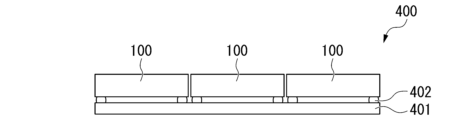
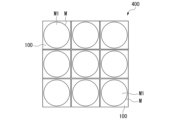
- the mirror array according to [14] wherein the distance between the mirror devices is 0.5 mm or less.
- a MEMS type optical switch device for optical fibers having a mirror array the mirror array having a plurality of mirror devices on a supporting substrate, the mirror devices being the mirror devices according to any one of [1] to [5] or [7] to [13].
- a MEMS type optical switch device for optical fibers having a mirror array the mirror array having a plurality of mirror devices on a supporting substrate, the mirror devices being the mirror device according to [6].
- a mirror is arranged on one side of a housing, and a functional layer including a first actuator and the second actuator is arranged on the other side of the housing. Therefore, the size of the mirror is not restricted by the installation area of the actuator, and a large-area mirror can be provided.
- the terminal portion is arranged on the surface of the functional layer opposite the housing, for example, when constructing a mirror array, the wiring on the supporting substrate side can be arranged directly below the mirror device. As a result, when arranging multiple mirror devices on a supporting substrate, etc., there is no need to provide wiring space on the supporting substrate between the mirror devices, and the mirror devices can be arranged closely together.
- the functional layer that drives the mirror has a first semiconductor layer, a second semiconductor layer, and an interlayer insulating layer, and is provided with a first actuator and a second actuator, and the first actuator and the second actuator each have a first comb-shaped electrode and a second comb-shaped electrode, respectively, so that the actuator can be made thinner and the structure of the actuator can be simplified.
- the orientation of the mirror can be freely changed by the first actuator and the second actuator.
- the functional layer has a first semiconductor layer, a second semiconductor layer, and an interlayer insulating layer, and the first and second comb-shaped electrodes of the first and second actuators are composed of these layers, making it possible to reduce the thickness of the actuators and simplify the structure of the actuators.
- the first movable part is attached to the second movable part via the first torsion beam part, and the second movable part is attached to the wiring part via the second torsion beam part. Therefore, the first movable part can be rotated in a first rotation direction and a second rotation direction, and the orientation of the mirror connected to the first movable part via the operating part can be freely changed.
- the first actuator is composed of a first comb-shaped electrode provided on the first movable part and a second comb-shaped electrode provided on the second movable part
- the first movable part can be rotated in a first rotation direction relative to the second movable part
- the second actuator is composed of a first comb-shaped electrode provided on the second movable part and a second comb-shaped electrode provided on the fixed part
- the second movable part can be rotated in a second rotation direction relative to the fixed part and the wiring part.
- first movable part to be rotated in the first rotation direction and the second rotation direction relative to the housing, and since the rotation amount in the first rotation direction and the second rotation direction can be changed individually by the first actuator and the second actuator, the orientation of the mirror connected to the first movable part can be freely changed.
- the fixed portion is divided into a plurality of divided regions, and a second comb-shaped electrode of the second actuator is provided in each divided region.
- Each divided region is further provided with a first via that electrically connects the first semiconductor layer and the second semiconductor layer that constitute the second comb-shaped electrode of the second actuator, and a first terminal portion.
- the first terminal portion is electrically connected to the first semiconductor layer and the second semiconductor layer that constitute the second comb-shaped electrode of the second actuator, so that a voltage for operating the second actuator can be applied from the first terminal portion arranged on the upper surface side of the functional layer.
- the first semiconductor layer of the second movable part is provided with a buried insulating layer that insulates and separates the second comb-shaped electrode of the first actuator from the first comb-shaped electrode of the second actuator, and is provided with a second via that connects the second semiconductor layer to the first semiconductor layer of the second comb-shaped electrode of the first actuator.
- the second terminal portion provided on the wiring portion is electrically connected to the first semiconductor layer and the second semiconductor layer that constitute the second comb-shaped electrode of the first actuator
- the third terminal portion provided on the wiring portion is electrically connected to the first semiconductor layer that constitutes the first comb-shaped electrode of the second actuator
- the third terminal portion is further electrically connected to the first semiconductor layer that constitutes the first comb-shaped electrode of the first actuator. Therefore, a voltage for operating the first actuator and the second actuator can be applied from the second terminal portion and the third terminal portion arranged on the upper surface side of the functional layer.
- the second terminal portion provided on the wiring portion is electrically connected to the second semiconductor layer constituting the second comb-shaped electrode of the first actuator
- the third terminal portion provided on the wiring portion is electrically connected to the first semiconductor layer constituting the first comb-shaped electrode of the second actuator and the first semiconductor layer constituting the second comb-shaped electrode of the first actuator
- the third terminal portion is further electrically connected to the first semiconductor layer constituting the first comb-shaped electrode of the first actuator. Therefore, a voltage for operating the first actuator and the second actuator can be applied from the second terminal portion and the third terminal portion arranged on the upper surface side of the functional layer.
- the fixed portion is divided into a plurality of divided regions, and a second comb-shaped electrode of the second actuator is provided in each divided region.
- the second semiconductor layer is divided into two regions, and one region of the divided second semiconductor layer constitutes the second comb-shaped electrode of the second actuator together with the first semiconductor layer.
- the other region of the second semiconductor layer is provided with a first via that electrically connects the second semiconductor layer and the first semiconductor layer that constitute the divided region, and a first terminal portion.
- the first terminal portion is electrically connected to the first semiconductor layer that constitutes the second comb-shaped electrode of the second actuator, so that a voltage for operating the second actuator can be applied from the first terminal portion arranged on the upper surface side of the functional layer.
- the first semiconductor layer of the second movable part is provided with a buried insulating layer that insulates and separates the second comb-shaped electrode of the first actuator from the first comb-shaped electrode of the second actuator, and a second via is provided that electrically connects the second semiconductor layer of the second movable part to the first semiconductor layer of the second comb-shaped electrode of the first actuator. Therefore, the first semiconductor layer constituting the second comb-shaped electrode of the first actuator and the first semiconductor layer constituting the first comb-shaped electrode of the second actuator, both formed in the second movable part, can be electrically separated, and the first actuator and the second actuator can be controlled individually.
- the second terminal portion provided on the wiring portion is electrically connected to the second semiconductor layer and the first semiconductor layer that constitute the second comb-shaped electrode of the first actuator
- the third terminal portion provided on the wiring portion is electrically connected to the first semiconductor layer that constitutes the first comb-shaped electrode of the second actuator
- the third terminal portion is further electrically connected to the first semiconductor layer that constitutes the first comb-shaped electrode of the first actuator. Therefore, a voltage for operating the first actuator and the second actuator can be applied from the second terminal portion and the third terminal portion arranged on the upper surface side of the functional layer.
- the mirror array described in the above [14] or [15] a plurality of mirrors can be arranged closely together.
- the mirror array described in [16] or [17] above since the mirror array is bonded to the supporting substrate via the bumps formed on the terminal portions, it is possible to reduce the wiring space on the supporting substrate.
- the distance between the mirror devices is 0.5 mm or less, so that the gap between the mirrors can be made small.
- the MEMS optical switch device described in [20] or [21] above since it is provided with a mirror array that allows a plurality of mirrors to be densely arranged, it is possible to realize a high-density and large-scale optical fiber changeover switch.
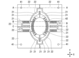
- FIG. 1A is a schematic plan view of a mirror device according to a first embodiment of the present invention.
- FIG. 1B is a schematic plan view showing a second semiconductor layer that constitutes the mirror device.
- FIG. 1C is a schematic plan view showing a first semiconductor layer that constitutes the mirror device.
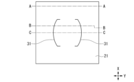
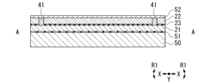
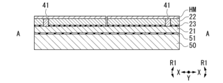
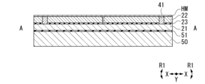
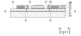
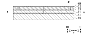
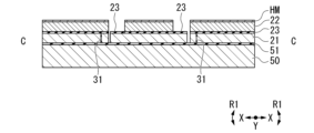
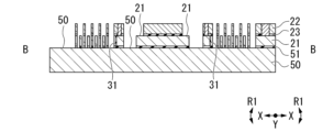
- FIG. 2 is a schematic cross-sectional view corresponding to line AA in FIG. 1A.
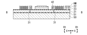
- FIG. 3 is a schematic cross-sectional view corresponding to line BB in FIG. 1A.
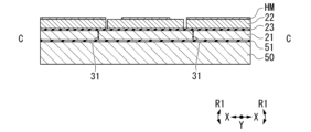
- FIG. 4 is a schematic cross-sectional view corresponding to line CC in FIG. 1A.
- 5 is an enlarged cross-sectional view of the buried insulating layer shown in FIG. 3.
- FIG. 6 is an enlarged cross-sectional view of the buried insulating layer shown in FIG.
- FIG. 7 is a schematic plan view of a mirror device according to a first embodiment of the present invention.
- FIG. 8 is a schematic cross-sectional view corresponding to line DD in FIG.
- FIG. 9 is a diagram for explaining the operation of the mirror device according to the first embodiment of the present invention, and is a schematic cross-sectional view corresponding to line CC in FIG. 1A.
- FIG. 10A is a schematic plan view illustrating a manufacturing method for a mirror device according to the first embodiment of the present invention.
- FIG. 10-2 is a schematic cross-sectional view corresponding to line AA in FIG. 10-1.
- FIG. 10-3 is a schematic cross-sectional view corresponding to line BB in FIG. 10-1.
- FIG. 10-4 is a schematic cross-sectional view corresponding to line CC in FIG. 10-1.
- FIG. 11A is a schematic plan view illustrating a manufacturing method for a mirror device according to the first embodiment of the present invention.
- FIG. 11-2 is a schematic cross-sectional view corresponding to line AA in FIG. 11-1.
- FIG. 11-3 is a schematic cross-sectional view corresponding to line BB in FIG. 11-1.
- FIG. 11-4 is a schematic cross-sectional view corresponding to line CC in FIG. 11-1.
- FIG. 12A is a schematic plan view illustrating a manufacturing method for a mirror device according to the first embodiment of the present invention.
- FIG. 12-2 is a schematic cross-sectional view corresponding to line AA in FIG. 12-1.
- FIG. 12-3 is a schematic cross-sectional view corresponding to line BB in FIG. 12-1.
- FIG. 12-4 is a schematic cross-sectional view corresponding to line CC in FIG. 12-1.
- FIG. 13A is a schematic plan view illustrating a manufacturing method for a mirror device according to the first embodiment of the present invention.
- FIG. 13-2 is a schematic cross-sectional view corresponding to line AA in FIG. 13-1.
- FIG. 13-3 is a schematic cross-sectional view corresponding to line BB in FIG. 13-1.
- FIG. 13-4 is a schematic cross-sectional view corresponding to line CC in FIG. 13-1.
- FIG. 14A is a schematic plan view illustrating a manufacturing method for a mirror device according to the first embodiment of the present invention.
- FIG. 14A is a schematic plan view illustrating a manufacturing method for a mirror device according to the first embodiment of the present invention.
- FIG. 14-2 is a schematic cross-sectional view corresponding to line AA in FIG. 14-1.
- FIG. 14-3 is a schematic cross-sectional view corresponding to line BB in FIG. 14-1.
- FIG. 14-4 is a schematic cross-sectional view corresponding to line CC in FIG. 14-1.
- FIG. 15A is a schematic plan view illustrating a manufacturing method for a mirror device according to the first embodiment of the present invention.
- FIG. 15-2 is a schematic cross-sectional view corresponding to line AA in FIG. 15-1.
- FIG. 15-3 is a schematic cross-sectional view corresponding to line BB in FIG. 15-1.
- FIG. 15-4 is a schematic cross-sectional view corresponding to line CC in FIG. 15-1.
- FIG. 15A is a schematic plan view illustrating a manufacturing method for a mirror device according to the first embodiment of the present invention.
- FIG. 15-2 is a schematic cross-sectional view corresponding to line AA in FIG. 15-1.
- FIG. 16A is a schematic plan view illustrating a manufacturing method for a mirror device according to the first embodiment of the present invention.
- FIG. 16-2 is a schematic cross-sectional view corresponding to line AA in FIG. 16-1.
- FIG. 16-3 is a schematic cross-sectional view corresponding to line BB in FIG. 16-1.
- FIG. 16-4 is a schematic cross-sectional view corresponding to line CC in FIG. 16-1.
- FIG. 17A is a schematic plan view illustrating a manufacturing method for a mirror device according to the first embodiment of the present invention.
- FIG. 17-2 is a schematic cross-sectional view corresponding to line AA in FIG. 17-1.
- FIG. 17-3 is a schematic cross-sectional view corresponding to line BB in FIG. 17-1.
- FIG. 17-4 is a schematic cross-sectional view corresponding to line CC in FIG. 17-1.
- FIG. 18 is a schematic plan view of a mirror device according to a second embodiment of the present invention.
- FIG. 19 is a schematic plan view of a mirror device according to a third embodiment of the present invention.
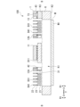
- FIG. 20 is a schematic side view of a mirror array according to the fourth embodiment of the present invention.
- FIG. 21 is a schematic plan view of a mirror array according to a fourth embodiment of the present invention.
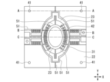
- the mirror device 100 of this embodiment includes at least a housing K, a mirror M, and a functional layer 1 disposed on the housing K to drive the mirror M. More specifically, the mirror device 100 of this embodiment includes a housing K having a cavity K1, a mirror M disposed on one surface K2 of the housing K, a functional layer 1 disposed on the other surface K3 of the housing K, and an operation unit K4 disposed in the cavity K1 of the housing K to connect the functional layer 1 and the mirror M.
- the housing K and the operation unit K4 are made of single crystal silicon and are, for example, cut out from a single crystal silicon substrate.
- the mirror M arranged on one surface K2 of the housing K has a reflecting surface M1 on the side opposite to the side on which the housing K is arranged.
- the functional layer 1 includes a first electrostatic actuator 2 that rotates the mirror M in a first rotation direction R1, a second electrostatic actuator 3 that rotates the mirror M in a second rotation direction R2 that intersects with the first rotation direction R1, and terminals T1 to T3 that are located on the surface 1A opposite the housing K.
- the first rotation direction R1 is a rotation direction with the Y direction as the rotation axis, as shown in Figures 2 to 4
- the second rotation direction R2 is a rotation direction with the X direction as the rotation axis, as shown in Figure 8.
- the X direction and the Y direction are perpendicular to each other on the same plane.
- the functional layer 1 is a multi-layer structure and includes a first semiconductor layer 21, a second semiconductor layer 22, and an interlayer insulating layer 23 disposed between the first semiconductor layer 21 and the second semiconductor layer 22.
- the first semiconductor layer 21 and the second semiconductor layer 22 are made of, for example, silicon layers, and the interlayer insulating layer 23 is made of, for example, a silicon oxide layer.
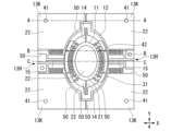
- the functional layer 1 is formed with a first movable portion 11, a second movable portion 12, a fixed portion 13K, a wiring portion 13H, a plurality of terminal portions T1, T2, and T3, a first torsion beam portion 14, and a second torsion beam portion 15.
- Figures 1B and 1C show schematic plan views of the second semiconductor layer 22 and the first semiconductor layer 21.
- the first movable portion 11, the second movable portion 12, the fixed portion 13K, the wiring portion 13H, the multiple terminal portions T1, T2, T3, the first torsion beam portion 14, and the second torsion beam portion 15 are formed in the functional layer 1 by processing the first semiconductor layer 21, the second semiconductor layer 22, and the interlayer insulating layer 23 into desired shapes using microfabrication techniques including photolithography. That is, the first movable portion 11, the second movable portion 12, the fixed portion 13K, the wiring portion 13H, and the second torsion beam portion 15 are composed of the first semiconductor layer 21, and the interlayer insulating layer 23 and the second semiconductor layer 22 that cover at least a part or all of the first semiconductor layer 21.
- the first torsion beam portion 14 is also composed of the first semiconductor layer 21.
- the functional layer 1 includes two first actuators 2 (2A, 2B) and four second actuators 3 (3A to 3D).
- the first actuators 2A, 2B and the second actuators 3A to 3D each have a first comb-shaped electrode D1 made of a first semiconductor layer 21 and a second comb-shaped electrode D2 made of the first semiconductor layer 21, an interlayer insulating layer 23 and a second semiconductor layer 22.
- the first actuators 2A, 2B and the second actuators 3A to 3D are formed together with the first movable portion 11, the second movable portion 12, the fixed portion 13K and the wiring portion 13H by microfabrication techniques including photolithography.
- the first actuators 2A and 2B are symmetrically positioned with respect to each other with respect to the first torsion beam portion 14, and the second actuators 3A, 3B and 3C, 3D are symmetrically positioned with respect to each other with respect to the second torsion beam portion 15.
- the following describes the functional layer 1, in particular the relationship between the first movable part 11, the second movable part 12, and the fixed part 13K and the first actuators 2A, 2B, and the second actuators 3A to 3D, and the relationship between the first comb-shaped electrode D1 and the second comb-shaped electrode D2 constituting each of the actuators 2A, 2B, 3A to 3D, and the first semiconductor layer 21, the interlayer insulating layer 23, and the second semiconductor layer 22.
- the first movable part 11 is located almost in the center of the functional layer 1, and the operation part K4 is joined to this first movable part 11.
- the mirror M is joined to the operation part K4.
- the first movable part 11 is a laminate of the first semiconductor layer 21, the interlayer insulating layer 23, and the second semiconductor layer 22, but in a part of the first movable part 11, the interlayer insulating layer 23 and the second semiconductor layer 22 are not laminated, and the first movable part 11 is composed only of the first semiconductor layer 21.
- the first comb-shaped electrode D1 (D11) constituting the first actuator 2 is provided in the part composed only of the first semiconductor layer 21, the first comb-shaped electrode D1 (D11) constituting the first actuator 2 is provided.
- the first comb-shaped electrode D11 in the first movable part 11 is arranged on both sides of the first movable part 11 in the X direction.
- the first comb-shaped electrode D11 protrudes in the X direction.
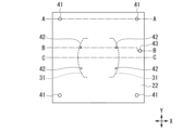
- the second movable part 12 is a ring-shaped member arranged to surround the first movable part 11.
- the second movable part 12 has a ring-shaped part 12A and four electrode parts 12B that protrude outward from the ring-shaped part 12A.
- the ring-shaped part 12A is made of a laminate of a first semiconductor layer 21, an interlayer insulating layer 23, and a second semiconductor layer 22, and is joined to the second torsion beam part 15.
- the electrode parts 12B are made of only the first semiconductor layer 21, and protrude from the ring-shaped part 12A.
- the first semiconductor layer 21 of the ring-shaped part 12A and the first semiconductor layer 21 of the electrode parts 12B are a continuous layer.
- second comb-like electrodes D2 constituting two sets of first actuators 2A, 2B are provided. These second comb-like electrodes D21 are arranged so as to face the two first comb-like electrodes D11 provided on the first movable portion 11, respectively.
- the second comb-like electrodes D21 are composed of a laminate of a first semiconductor layer 21, an interlayer insulating layer 23, and a second semiconductor layer 22.
- the four electrode portions 12B of the second movable portion 12 are provided with the first comb-like electrodes D1 (D31) of the second actuators 3A to 3D.
- the first comb-like electrodes D31 are made only of the first semiconductor layer 21.
- the first comb-like electrodes D31 in the second movable portion 12 are provided so as to protrude from the electrode portions 12B in the Y direction.
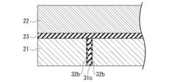
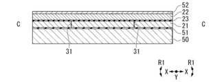
- the first semiconductor layer 21 of the annular portion 12A is provided with a buried insulating layer 31.
- the buried insulating layer 31 is provided to divide the first semiconductor layer 21 into two regions.
- the buried insulating layer 31 is an insulating layer for electrically insulating and isolating the first semiconductor layer 21 constituting the second comb-shaped electrodes D21 of the first actuators 2A and 2B located inside the annular portion 12A from the first semiconductor layer 21 constituting the first comb-shaped electrodes D31 of the second actuators 3A to 3D located in the electrode portion 12B on the outside of the annular portion 12A.
- FIG. 5 and 6 show enlarged cross-sectional views of the buried insulating layer 31.
- FIG. 5 is an enlarged cross-sectional view of the buried insulating layer 31 in FIG. 3.
- FIG. 6 is an enlarged cross-sectional view of the buried insulating layer 31 in FIG. 4.
- the buried insulating layer 31 is formed by forming a wall surface insulating layer 32b and a filling layer 31c inside a trench groove 31a provided in the first semiconductor layer 21.
- the wall surface insulating layer 32b is made of, for example, silicon nitride
- the filling layer 31c is made of, for example, polysilicon.
- the buried insulating layer 31 thus formed surrounds a part of the inner periphery of the annular portion 12A, as shown in FIG. 1A.
- the second comb-shaped electrode D21 of the first actuator 2A, 2B and the second via 42 are arranged in the area surrounded by the buried insulating layer 31.
- the second movable portion 12 is provided with a second via 42 penetrating the second semiconductor layer 22 and the interlayer insulating layer 23.
- the second via 42 is provided to electrically connect the second semiconductor layer 22 of the second movable portion 12 to the first semiconductor layer 21. More specifically, the second via 42 is provided at a position within the region divided by the embedded insulating layer 31 where it is possible to electrically connect the first semiconductor layer 21 constituting the second comb-shaped electrode D21 of the first actuators 2A and 2B to the second semiconductor layer 22.
- the second via 42 is made of, for example, polycrystalline silicon or metal.
- the fixed portion 13K is disposed so as to surround the second movable portion 12, and is joined to the other surface K3 of the housing K.
- the entire functional layer 1 is disposed on the other surface K3 of the housing K.
- the fixed portion 13K is composed of a laminate in which a first semiconductor layer 21, a second semiconductor layer 22, and an interlayer insulating layer 23 are stacked.
- the fixed portion 13K is divided into four divided regions 13A to 13D. That is, as shown in FIG. 1A and FIG.
- the divided regions 13A to 13D are insulated and separated from each other because the first semiconductor layer 21, the second semiconductor layer 22, and the interlayer insulating layer 23 are not continuous between adjacent divided regions, and a lower insulating layer 51 is disposed between the housing K and the first semiconductor layer 21. Additionally, each of the divided regions 13A to 13D of the fixed portion 13K is also insulated and separated from the wiring portion 13H.
- the second comb-like electrodes D2 (D41) of the second actuators 3A to 3D are provided in each divided region 13A to 13D of the fixed portion 13K.
- the second comb-like electrodes D41 are composed of a laminate of a first semiconductor layer 21, an interlayer insulating layer 23, and a second semiconductor layer 22.
- the second comb-like electrodes D41 in the fixed portion 13K protrude in the Y direction, and thus face the first comb-like electrodes D31 provided in the electrode portion 12B of the second movable portion 12.
- the split regions 13A to 13D of the fixed portion 13K are each provided with a first via 41 penetrating the second semiconductor layer 22 and the interlayer insulating layer 23.
- the first via 41 electrically connects the first semiconductor layer 21 constituting the second comb-shaped electrode D41 of the second actuator 3A to 3D to the second semiconductor layer 22 constituting each split region 13A to 13D.
- the first via 41 is exposed on the surface of the second semiconductor layer 22, and the surface of this first via 41 is used as the first terminal portion T1.
- the first terminal portion T1 is located on the first via 41 and is on the same plane as the surface of the second semiconductor layer 22.
- the first via 41 is made of, for example, polycrystalline silicon or metal.
- the first terminal portion T1 is electrically connected to the second semiconductor layer 22 constituting the second comb-shaped electrode D2 (D41) of the second actuator 3A to 3D, and is electrically connected to the first semiconductor layer 21 constituting the second comb-shaped electrode D2 (D41) of the second actuator 3A to 3D through the first via 41.
- the wiring portion 13H is disposed in a position surrounding the second movable portion 12, similar to the fixed portion 13K, and is particularly adjacent to the second movable portion 12.
- the functional layer 1 is disposed on the other surface K3 side of the housing K.
- the wiring portion 13H is composed of a laminate made of a first semiconductor layer 21, an interlayer insulating layer 23 laminated on a portion of the first semiconductor layer 21, and a second semiconductor layer 22.
- the second semiconductor layer 22 constituting the wiring portion 13H is divided into two regions, and the second terminal portion T2 is provided in one of the regions.
- the second terminal portion T2 is electrically insulated from the first semiconductor layer 21 of the wiring portion 13H by the interlayer insulating layer 23.
- a third via 43 is formed in the other region of the divided second semiconductor layer, and a third terminal portion T3 is provided on the third via 43 and the second semiconductor layer 22.
- the third via 43 penetrates the interlayer insulating layer 23 to electrically connect the first semiconductor layer 21 and the second semiconductor layer 22.
- the third terminal portion T3 is electrically connected to the first semiconductor layer 21 of the wiring portion 13H, while being electrically isolated from the second terminal portion T2.
- the second torsion beam portion 15 is a member that connects the second movable portion 12 and the wiring portion 13H, and extends in the rotation axis direction (x direction) of the second rotation direction R2.
- the second torsion beam portion 15 is composed of a laminate of a first semiconductor layer 21, a second semiconductor layer 22, and an interlayer insulating layer 23.
- One end of the second torsion beam portion 15 is connected to the wiring portion 13H.
- the second terminal portion T2 is electrically connected to the second semiconductor layer 22 of the second torsion beam portion 15, and the third terminal portion T3 is electrically connected to the first semiconductor layer 21 of the second torsion beam portion 15.
- the other end of the second torsion beam portion 15 is connected to the second movable portion 12 as described above.
- the first torsion beam portion 14 is a member that connects the first movable portion 11 and the second movable portion 12, and extends in the rotation axis direction (Y direction) of the first rotation direction R1.
- the first torsion beam portion 14 is composed only of the first semiconductor layer 21.
- the second terminal portion T2 is electrically connected to the first semiconductor layer 21 and the second semiconductor layer 22 that constitute the second comb-shaped electrode D2 (D21) of the first actuator 2A, 2B via the second semiconductor layer 22 that constitutes the second torsion beam portion 15, the second semiconductor layer 22 of the second movable portion, and the second via 42.
- the third terminal portion T3 is electrically connected via the first semiconductor layer 21 of the second torsion beam portion 15 to the first semiconductor layer 21 constituting the first comb-shaped electrode D1 (D31) of the second actuator. Furthermore, the third terminal portion T3 is electrically connected to the first semiconductor layer 21 constituting the first comb-tooth electrode D1 (D11) of the first actuator 2A, 2B via the first semiconductor layer 21 of each of the second torsion beam portion 15, the second movable portion 12, and the first torsion beam portion 14.
- the first actuators 2A to 2B are configured by arranging a first comb-like electrode D11 provided on the first movable portion 11 and a second comb-like electrode D21 provided on the second movable portion 12 so as to face each other.
- the second actuators 3A to 3D are configured by arranging a first comb-like electrode D31 provided on the second movable portion 12 and a second comb-like electrode D41 provided on the fixed portion 13K so as to face each other.
- the first comb-like electrodes D11 and D31 of each of the actuators 2A, 2B, 3A to 3D are made of only the first semiconductor layer 21, and the second comb-like electrodes D21 and D41 of each of the actuators 2A, 2B, 3A to 3D are made of the first semiconductor layer 21, the second semiconductor layer 22, and the interlayer insulating layer 23.
- the first comb-like electrodes D11, D31 and the second comb-like electrodes D21, D41 are located at approximately the same height in the thickness direction of the functional layer 1. However, the thickness of the second comb-like electrodes D21, D41 is greater than that of the first comb-like electrodes D11, D31.
- first movable part 11 When the first movable part 11 is rotated in the first rotation direction R1 by the first actuators 2A and 2B, a height displacement occurs between the first movable part 11 and the second movable part 12 in one of the first actuators 2A and 2B.
- the first comb-shaped electrode D11 of the first actuator 2A on the right side of FIG. 2 is displaced upward in FIG. 2. This causes the entire first movable part 11 to tilt, and since the first actuators 2A and 2B are located symmetrically with respect to the first torsion beam part 14, a twist occurs in the first torsion beam part 14 connecting the first movable part 11 and the second movable part 12.
- FIG. 9 shows the state in which the first movable part 11 is rotated in the first rotation direction R1 relative to the second movable part 12 by the first actuator 2A (right side). To obtain rotation in the opposite direction, the first actuator 2B (left side) is driven.
- the second movable part 12 when the second movable part 12 is rotated in the second rotation direction R2 by the second actuators 3A to 3D, a height displacement is generated between the second movable part 12 and the fixed part 13K in either the pair of second actuators 3A and 3C or the pair of second actuators 3B and 3D among the second actuators 3A to 3D.
- the first comb-shaped electrodes D31 of the two second actuators 3A and 3C on the upper side of FIG. 1A are displaced toward the front of the paper in FIG. 1A.
- the second actuators 3B and 3D are used.
- the second movable part 12 is tilted, and since the second actuators 3A to 3D are located symmetrically with respect to the second torsion beam part 15, a twist is generated in the second torsion beam part 15 connecting the second movable part 12 and the wiring part 13H. In this way, the second actuators 3A to 3D make it possible to rotate the second movable part 12 in the second rotation direction R2 relative to the fixed part 13K.
- the first actuators 2A, 2B can rotate the first movable part 11 in the first rotation direction R1 relative to the second movable part 12, and the second actuators 3A-3D can rotate the second movable part 12 in the second rotation direction R2 relative to the fixed part 13K and the wiring part 13H, so that the first movable part 11 can be rotated in the first rotation direction R1 and the second rotation direction R2.
- the first actuators 2A, 2B and the second actuators 3A-3D can change the amount of rotation in the first rotation direction R1 and the second rotation direction R2 individually, so that the orientation of the reflective surface M1 of the mirror M connected to the first movable part 11 can be freely changed relative to the housing K.
- a first driving voltage is applied to the second semiconductor layer 22 from the second terminal T2.
- the first driving voltage applied to the second semiconductor layer 22 from the second terminal T2 reaches the second semiconductor layer 22 of the second movable portion 12 via the second torsion beam portion 15, and is applied directly to the second semiconductor layer 22 constituting the second comb-shaped electrodes D21 of the first actuators 2A and 2B provided in the second movable portion 12.
- the first driving voltage that reaches the second semiconductor layer 22 of the second movable portion 12 is also applied to the first semiconductor layer 21 constituting the second comb-shaped electrodes D21 of the first actuators 2A and 2B via the second via 42.
- the first driving voltage is not applied to the first comb-shaped electrodes D31 of the second actuators 3A to 3D.
- a third drive voltage is applied to the third terminal T3.
- the third drive voltage is a voltage having a different voltage value from the first drive voltage, and may be a ground voltage.
- the third drive voltage applied from the third terminal T3 reaches the first semiconductor layer 21 of the second movable part 12 via the first semiconductor layer 21 of the second torsion beam part 15, and is applied to the first semiconductor layer 21 of the first movable part 11, i.e., the first comb-shaped electrode D1 (D11) of the first actuators 2A and 2B via the first torsion beam part 14. This displaces the first comb-shaped electrode D1 (D11) of the first actuator 2A or 2B.
- the third drive voltage is also applied to the first semiconductor layer 21 constituting the second comb-shaped electrode D41 of the second actuators 3A to 3D.
- the first actuators 2A and 2B can be operated by applying a first drive voltage to the second comb-shaped electrodes D21 of the first actuators 2A and 2B and applying a third drive voltage (e.g., ground voltage) to the first comb-shaped electrodes D11.
- a third drive voltage e.g., ground voltage
- a second drive voltage is applied from the first terminal T1 to the second semiconductor layer 22 of the fixed portion 13K.
- the second drive voltage may be a voltage having the same voltage value as the first drive voltage, or may be a voltage having a different voltage value.
- the second drive voltage is a voltage having a different voltage value from the third drive voltage.
- the second drive voltage applied from the first terminal T1 to the second semiconductor layer 22 is applied as is to the second semiconductor layer 22 constituting the second comb-shaped electrodes D41 of the second actuators 3A to 3D provided in the division regions 13A to 13D.
- the second drive voltage applied to the second semiconductor layer 22 is also applied to the first semiconductor layer 21 constituting the second comb-shaped electrodes D41 of the second actuators 3A to 3D via the first vias 41.
- the third drive voltage (e.g., ground voltage) applied to the third terminal T3 is also applied to the first semiconductor layer 21 constituting the first comb-shaped electrodes D31 of the second actuators 3A to 3D. This displaces the first comb-shaped electrodes D31 of the second actuators 3A to 3D.
- the second actuators 3A to 3D can be operated by applying the second drive voltage to the second comb-shaped electrodes D41 of the second actuators 3A to 3D and applying the third drive voltage (e.g., ground voltage) to the first comb-shaped electrodes D31.
- the third drive voltage e.g., ground voltage
- a substrate is prepared in which a support substrate 50, a lower insulating layer 51, and a first semiconductor layer 21 are laminated.
- This may be prepared by film formation, or an SOI substrate may be used.
- the support substrate 50 is, for example, a silicon substrate
- the lower insulating layer 51 is, for example, a silicon oxide layer
- the first semiconductor layer 21 is, for example, a silicon layer.
- the buried insulating layer 31 is formed in this first semiconductor layer 21.
- the buried insulating layer 31 is formed by forming a trench groove in the first semiconductor layer 21, then forming an insulating film that will become the wall surface insulating layer 32b on the first semiconductor layer 21 and in the trench groove, then forming a polysilicon layer that will become the filling layer 31c on the first semiconductor layer 21 and in the trench groove, and removing the insulating film and polysilicon layer stacked on the first semiconductor layer 21 to form the buried insulating layer 31 as shown in detail in Figures 5 and 6.
- an interlayer insulating layer 23 and a second semiconductor layer 22 are formed on the first semiconductor layer 21.
- the interlayer insulating layer 23 is, for example, a silicon oxide layer
- the second semiconductor layer is, for example, a silicon layer.
- the interlayer insulating layer 23 and the second semiconductor layer 22 may be formed by a normal film forming technique, or may be formed by bonding an SOI substrate.
- a first via 41 and a second via 42 are formed at a predetermined position of the second semiconductor layer 22.
- the first via 41 and the second via 42 are formed by forming a through hole penetrating the second semiconductor layer 22 and the interlayer insulating layer 23, and filling the through hole with, for example, polysilicon or metal.
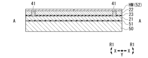
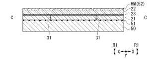
- an upper insulating layer 52 is formed on the second semiconductor layer 22.
- the upper insulating layer 52 is, for example, made of a silicon oxide layer.
- This upper insulating layer 52 becomes a hard mask layer for forming each part of the functional layer 1.
- the upper insulating layer 52 may be referred to as a hard mask layer HM.
- the upper insulating layer 52 is partially etched to a depth of about 1/4 to 1/3 of its film thickness, thereby forming the upper insulating layer 52 into a hard mask layer HM having a cross-sectional shape as shown in Figures 12-2 to 12-4. Note that the illustration of the hard mask layer HM is omitted in Figure 12-1.
- the hard mask layer HM (upper insulating layer 52) is partially etched to a depth of about 1/4 to 1/3 of the original film thickness, so that the upper insulating layer 52 becomes a hard mask layer HM with a cross-sectional shape as shown in Figures 13-2 to 13-4.
- the hard mask layer HM is formed into a relatively thick portion and a relatively thin portion, and further, a portion where the hard mask layer HM does not exist is also formed.
- the relatively thick portion of the hard mask layer HM will ultimately be the portion where the first semiconductor layer 21, the second semiconductor layer 22, and the interlayer insulating layer 23 remain.
- the relatively thin portion of the hard mask layer HM will ultimately be the portion where the first semiconductor layer 21 remains and the second semiconductor layer 22 and the interlayer insulating layer 23 are removed. Furthermore, the portions where the hard mask layer HM does not exist will ultimately be portions where the first semiconductor layer 21, the second semiconductor layer 22, and the interlayer insulating layer 23 are all removed.
- the second semiconductor layer 22 is partially removed by etching using the hard mask layer HM as a mask.
- the portions from which the second semiconductor layer 22 is removed correspond to the portions in Figs. 13-1 to 13-4 where the hard mask layer HM is not present.
- the interlayer insulating layer 23 that is partially exposed by removing the second semiconductor layer 22 is removed by etching. At this time, part of the hard mask layer HM is also removed.
- the hard mask layer HM that remains at this stage corresponds to the relatively thick part in Figs. 13-1 to 13-4.
- the lower insulating layer 51 that is partially exposed by removing the first semiconductor layer 21 is removed by etching. At this time, all remaining parts of the hard mask layer HM are removed. At this stage, the first movable portion 11, the second movable portion 12, the fixed portion 13K, the wiring portion 13H, the first torsion beam portion 14, and the second torsion beam portion 15 of the functional layer 1 are formed.
- a cavity K1 and an operating portion K4 are formed by removing a portion of the single crystal silicon substrate 50. Then, the lower insulating layer 51 exposed by removing the portion of the single crystal silicon substrate 50 is removed to form the functional layer 1. Furthermore, a mirror M is attached to the operating portion K4. Through these steps, the mirror device 100 shown in Figures 1A to 8 is manufactured.
- the above describes one example of a method for manufacturing the mirror device 100.
- the mirror device 100 of this embodiment is not limited to being manufactured by the above manufacturing method.
- a mirror M is arranged on one surface K2 side of the housing K, and a functional layer 1 including the first actuators 2A, 2B and the second actuators 3A to 3D is arranged on the other surface K3 side of the housing K, so that the size of the mirror M is not restricted by the installation area of the actuators 2A to 3D, and a large-area mirror M can be provided. Furthermore, since multiple terminal portions (first terminal portion T1, second terminal portion T2, third terminal portion T3) are arranged on the surface of the functional layer 1 opposite the housing K, for example, when constructing a mirror array, the wiring on the supporting substrate side can be arranged directly below the mirror device 100. As a result, when arranging multiple mirror devices 100 on a supporting substrate, etc., there is no need to provide wiring space on the supporting substrate between the mirror devices 100, and the mirror devices 100 can be arranged closely together.
- the functional layer 1 has the first semiconductor layer 21, the second semiconductor layer 22, and the interlayer insulating layer 23, and the first comb-shaped electrode D1 and the second comb-shaped electrode D2 of the first actuators 2A, 2B and the second actuators 3A to 3D are composed of these layers 21 to 23, so that the actuators 2A to 3D can be made thinner and the structure of the actuators 2A to 3D can be simplified.
- the functional layer 1 that drives the mirror M has a first semiconductor layer 21, a second semiconductor layer 22 and an interlayer insulating layer 23, and is provided with first actuators 2A, 2B and second actuators 3A to 3D, and the first actuators 2A, 2B and the second actuators 3A to 3D each have a first comb-tooth electrode D1 and a second comb-tooth electrode D2, thereby making it possible to reduce the thickness of the actuators, reduce the thickness of the actuators 2A to 3D, and simplify the structure of the actuators 2A to 3D.
- the orientation of the mirror M can be freely changed by the first actuators 2A and 2B and the second actuators 3A to 3D.
- the first movable part 11 is attached to the second movable part 12 via the first torsion beam part 14, and the second movable part 12 is attached to the wiring part 13H via the second torsion beam part 15. Therefore, the first movable part 11 can be rotated in the first rotation direction R1 and the second rotation direction R2, and the orientation of the mirror M connected to the first movable part 11 via the operating part K4 can be freely changed.
- the first actuators 2A, 2B are composed of a first comb-tooth electrode D11 provided on the first movable part 11 and a second comb-tooth electrode D21 provided on the second movable part 12, so that the first movable part 11 can be rotated in a first rotation direction R1 relative to the second movable part 12.
- the second actuators 3A to 3D are composed of a first comb-tooth electrode D31 provided on the second movable part 12 and a second comb-tooth electrode D41 provided on the fixed part 13K, so that the second movable part 12 can be rotated in a second rotation direction R2 relative to the fixed part 13K and the wiring part 13H.
- first movable part 11 rotate in the first rotation direction R1 and the second rotation direction R2 relative to the housing K, and the amount of rotation in the first rotation direction R1 and the second rotation direction R2 can be changed individually by the first actuators 2A, 2B and the second actuators 3A-3D, so that the orientation of the mirror M connected to the first movable part 11 can be freely changed.
- the fixed portion 13K is divided into four divided regions 13A to 13D, and each divided region 13A to 13D is provided with a first via 41 that connects the first semiconductor layer 21 and the second semiconductor layer 22 that constitute the second comb-shaped electrode D41 of the second actuator 3A to 3D, and a first terminal portion T1, so that a voltage for operating the second actuator 3A to 3D can be applied from the upper surface side of the functional layer 1.
- the first semiconductor layer 21 of the second movable portion 12 is provided with a buried insulating layer 31 that insulates and separates the second comb-shaped electrode D21 of the first actuators 2A and 2B from the first comb-shaped electrode D31 of the second actuators 3A to 3D, and is provided with a second via 42 that connects the second semiconductor layer 22 to the first semiconductor layer 21 of the second comb-shaped electrode D21 of the first actuators 2A and 2B.
- the second terminal T2 provided on the wiring portion 13H is electrically connected to the first semiconductor layer 21 and the second semiconductor layer 22 that constitute the second comb-shaped electrode D21 of the first actuators 2A and 2B
- the third terminal T3 provided on the wiring portion 13H is electrically connected to the first semiconductor layer 21 that constitutes the first comb-shaped electrode D31 of the second actuators 3A to 3D
- the third terminal T3 is further electrically connected to the first semiconductor layer 21 that constitutes the first comb-shaped electrode D11 of the first actuators 2A and 2B. Therefore, a voltage for operating the first actuators 2A, 2B and the second actuators 3A to 3D can be applied from the second terminal T2 and the third terminal T3 arranged on the upper surface side of the functional layer 1.
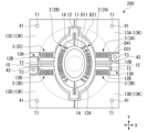
- a mirror device 200 according to a second embodiment of the present invention shows a schematic plan view of the mirror device 200 according to the second embodiment.
- the differences between the mirror device 200 of this embodiment and the mirror device 100 of the first embodiment are as follows.
- the second movable portion 12 is not provided with anything equivalent to the second via 42 and embedded insulating layer 31 of the mirror device 100.
- the rest of the structure is the same as that of the mirror device 100 of the first embodiment.
- the operation when a voltage is applied to the second terminal portion T2 and the third terminal portion T3 differs from that of the first embodiment.
- the second movable portion 12 of the mirror device 200 of this embodiment is a ring-shaped member arranged to surround the first movable portion 11.
- the second movable portion 12 has a ring-shaped portion 12A and four electrode portions 12B that protrude outward from the ring-shaped portion 12A.
- the ring-shaped portion 12A is made of a laminate of a first semiconductor layer 21, an interlayer insulating layer 23, and a second semiconductor layer 22, and is joined to the second torsion beam portion 15.
- the electrode portions 12B are made of only the first semiconductor layer 21.
- the first semiconductor layer 21 of the ring-shaped portion 12A and the first semiconductor layer 21 of the electrode portions 12B are continuous layers.
- second comb-like electrodes D2 constituting two sets of first actuators 2A, 2B are provided. These second comb-like electrodes D21 are arranged so as to face the two first comb-like electrodes D11 provided on the first movable portion 11, respectively.
- the second comb-like electrodes D21 are composed of a laminate of a first semiconductor layer 21, an interlayer insulating layer 23, and a second semiconductor layer 22.
- the four electrode portions 12B of the second movable portion 12 are provided with the first comb-like electrodes D1 (D31) of the second actuators 3A to 3D.
- the first comb-like electrodes D31 are made only of the first semiconductor layer 21.
- the first comb-like electrodes D31 in the second movable portion 12 are provided so as to protrude from the electrode portions 12B in the Y direction.
- the first movable portion 11 and the fixed portion 13K have the same configuration as in the first embodiment. Therefore, the first terminal portion T1 is electrically connected to the second semiconductor layer 22 constituting the second comb-shaped electrode D2 (D41) of the second actuator 3A to 3D, as in the first embodiment, and is electrically connected to the first semiconductor layer 21 constituting the second comb-shaped electrode D2 (D41) of the second actuator 3A to 3D through the first via 41.
- the wiring portion 13H, the first torsion beam portion 14, and the second torsion beam portion 15 are configured in the same manner as in the first embodiment.
- the second terminal portion T2 is electrically connected to the second semiconductor layer 22 constituting the second comb-shaped electrode D2 (D21) of the first actuator 2A, 2B via the second semiconductor layer 22 constituting the second torsion beam portion 15 and the second semiconductor layer 22 of the second movable portion.
- the third terminal portion T3 is electrically connected via the first semiconductor layer 21 of the second torsion beam portion 15 to the first semiconductor layer 21 constituting the first comb-tooth electrode D1 (D31) of the second actuators 3A to 3D and the first semiconductor layer 21 constituting the second comb-tooth electrode D2 (D21) of the first actuators 2A and 2B. Furthermore, the third terminal portion T3 is electrically connected to the first semiconductor layer 21 constituting the first comb-tooth electrode D1 (D11) of the first actuator 2A, 2B via the first semiconductor layer 21 of each of the second torsion beam portion 15, the second movable portion 12, and the first torsion beam portion 14.
- a method of applying voltages to operate the actuators 2A, 2B, and 3A to 3D in the mirror device 200 of this embodiment will be described in more detail.
- a first driving voltage is applied from the second terminal T2 to the second semiconductor layer 22.
- the first driving voltage applied from the second terminal T2 to the second semiconductor layer 22 reaches the second semiconductor layer 22 of the second movable portion 12 via the second torsion beam portion 15, and is applied directly to the second semiconductor layer 22 constituting the second comb-shaped electrodes D21 of the first actuators 2A and 2B provided on the second movable portion 12.
- a third driving voltage is applied to the third terminal T3.
- the third driving voltage is a voltage having a different voltage value from the first driving voltage, and may be a ground voltage.
- the third driving voltage applied from the third terminal T3 reaches the first semiconductor layer 21 of the second movable part 12 via the first semiconductor layer 21 of the second torsion beam part 15, and is applied directly to the first semiconductor layer 21 constituting the second comb-shaped electrode D21 of the first actuators 2A and 2B provided on the second movable part 12.
- this third driving voltage is applied to the first semiconductor layer 21 of the first movable part 11, i.e., the first comb-shaped electrode D1 (D11) of the first actuators 2A and 2B via the first torsion beam part 14. As a result, the first comb-shaped electrode D1 (D11) of the first actuator 2A or 2B is displaced.
- the first actuators 2A and 2B can be operated by applying a first drive voltage to the second semiconductor layer 22 of the second comb-shaped electrode D21 of the first actuators 2A and 2B and applying a third drive voltage (e.g., ground voltage) to the first comb-shaped electrode D11.
- a third drive voltage e.g., ground voltage
- a second drive voltage is applied to the second semiconductor layer 22 from the first terminal T1.
- the second drive voltage may be a voltage having the same voltage value as the first drive voltage, or may be a voltage having a different voltage value.
- the second drive voltage is a voltage having a different voltage value from the third drive voltage.
- the second drive voltage applied to the second semiconductor layer 22 from the first terminal T1 is applied as is to the second semiconductor layer 22 constituting the second comb-shaped electrodes D41 of the second actuators 3A to 3D provided in the division regions 13A to 13D.
- the second drive voltage applied to the second semiconductor layer 22 is also applied to the first semiconductor layer 21 constituting the second comb-shaped electrodes D41 of the second actuators 3A to 3D via the first vias 41.
- the third drive voltage (e.g., ground voltage) applied to the third terminal T3 to drive the first actuators 2A and 2B is also applied to the first semiconductor layer 21 constituting the first comb-shaped electrodes D31 of the second actuators 3A to 3D.
- the first comb-shaped electrodes D31 of the second actuators 3A to 3D are displaced.
- the second actuators 3A to 3D can be operated by applying the second drive voltage to the second comb-shaped electrodes D41 of the second actuators 3A to 3D and applying, for example, a third drive voltage (for example, a ground voltage) to the first comb-shaped electrodes D31. Note that it is sufficient to operate only the second actuators 3A and 3C or the second actuators 3B and 3D, rather than all of the second actuators 3A to 3D.
- the mirror device 200 of this embodiment can freely displace the mirror, similar to the first embodiment.
- the second terminal T2 provided on the wiring portion 13H is electrically connected to the second semiconductor layer 22 constituting the second comb-shaped electrode D2 (D21) of the first actuator 2A, 2B
- the third terminal T3 provided on the wiring portion 12H is electrically connected to the first semiconductor layer 21 constituting the first comb-shaped electrode D1 (D31) of the second actuator 3A to 3D and the first semiconductor layer 21 constituting the second comb-shaped electrode D2 (D21) of the first actuator 2A, 2B
- the third terminal T3 is further electrically connected to the first semiconductor layer 21 constituting the first comb-shaped electrode D1 ((D11)) of the first actuator 2A, 2B. Therefore, a voltage for operating the first actuator 2A, 2B and the second actuator 3A to 3D can be applied from the second terminal T2 and the third terminal T3 arranged on the upper surface side of the functional layer 1.
- a mirror device 300 according to a third embodiment of the present invention shows a schematic plan view of the mirror device 300 according to the third embodiment.
- the differences between the mirror device 300 of this embodiment and the mirror device 100 of the first embodiment are as follows.
- the second semiconductor layer 22 constituting the fixed portion 13K is divided into two regions.
- the rest of the structure is the same as that of the mirror device 100 of the first embodiment.
- the operation when a voltage is applied to the second terminal portion T2 and the third terminal portion T3 differs from that of the first embodiment.
- the fixed portion 13K of the mirror device 200 of this embodiment is disposed so as to surround the second movable portion 12, and is joined to the other surface K3 side of the housing K.
- the entire functional layer 1 is disposed on the other surface K3 side of the housing K.
- the fixed portion 13K is composed of a laminate in which the first semiconductor layer 21, the second semiconductor layer 22, and the interlayer insulating layer 23 are laminated.
- the fixed portion 13K is divided into four divided regions 13A to 13D.
- the divided regions 13A to 13D are insulated and separated from each other because the first semiconductor layer 21, the second semiconductor layer 22, and the interlayer insulating layer 23 are not continuous between the adjacent divided regions, and a lower insulating layer 51 is disposed between the housing K and the first semiconductor layer 21.
- the divided regions 13A to 13D are also insulated and separated from the wiring portion 13H.
- the second comb-like electrode D2 (D41) of the second actuator 3A to 3D is provided in each divided region 13A to 13D.
- This second comb-like electrode D41 is composed of a laminate of a first semiconductor layer 21, an interlayer insulating layer 23, and a second semiconductor layer 22.
- the second comb-like electrode D41 in the fixed portion 13K protrudes in the Y direction, and thus faces the first comb-like electrode D31 provided in the electrode portion 12B of the second movable portion 12.
- the second semiconductor layer 22 constituting the fixed portion 13K is divided into two regions.
- a first via 41 is provided in the other region of the second semiconductor layer 22, penetrating the interlayer insulating layer 23, to electrically connect the second semiconductor layer 22 and the first semiconductor layer 21 constituting that region. Further, a first terminal portion T1 connected to the first via 41 is provided in each divided region 13A to 13D of the fixed portion 13K. The first terminal portion T1 is located in the other region of the second semiconductor layer 22, similar to the first via 41. The first via 41 electrically connects the first terminal portion T1 provided in each divided region 13A to 13D to the first semiconductor layer 21 constituting the second comb-shaped electrode D41 of the second actuator 3A to 3D.
- the first via 41 is made of, for example, polycrystalline silicon or metal.
- the first terminal portion T1 is electrically connected through the first via 41 to the first semiconductor layer 21 that constitutes the second comb-shaped electrode D2 (D41) of the second actuator 3A-3D, but is not electrically connected to the second semiconductor layer 22 that constitutes the second comb-shaped electrode D2 (D41).
- the first movable portion 11, the second movable portion 12, the fixed portion 13K and the wiring portion 13H have the same configuration as in the first embodiment. Therefore, the second terminal portion T2 is electrically connected to the second semiconductor layer 22 and the first semiconductor layer 21 that constitute the second comb-shaped electrode D2 (D21) of the first actuators 2A and 2B, as in the first embodiment.
- the third terminal portion T3 is electrically connected to the first semiconductor layer 21 that constitutes the first comb-shaped electrode D1 (D31) of the second actuators 3A to 3D.
- the third terminal portion T3 is also electrically connected to the first semiconductor layer 21 that constitutes the first comb-shaped electrode D1 (D11) of the first actuators 2A and 2B.
- a method of applying voltages to operate the actuators 2A, 2B, and 3A to 3D in the mirror device 300 of this embodiment will now be described in more detail.
- a first driving voltage is applied to the second semiconductor layer 22 from the second terminal T2.
- the first driving voltage applied to the second semiconductor layer 22 from the second terminal T2 reaches the second semiconductor layer 22 of the second movable portion 12 via the second torsion beam portion 15, and is applied directly to the second semiconductor layer 22 constituting the second comb-shaped electrodes D21 of the first actuators 2A and 2B provided in the second movable portion 12.
- the first driving voltage that reaches the second semiconductor layer 22 of the second movable portion 12 is also applied to the first semiconductor layer 21 constituting the second comb-shaped electrodes D21 of the first actuators 2A and 2B via the second via 42.
- the first driving voltage is not applied to the first comb-shaped electrodes D31 of the second actuators 3A to 3D.
- a second drive voltage is applied to the third terminal T3.
- the second drive voltage is a voltage having a different voltage value from the first drive voltage.
- the second drive voltage applied from the third terminal T3 reaches the first semiconductor layer 21 of the second movable part 12 via the first semiconductor layer 21 of the second torsion beam part 15, and is applied to the first semiconductor layer 21 of the first movable part 11, that is, the first comb-shaped electrode D1 (D11) of the first actuators 2A and 2B via the first torsion beam part 14.
- the second drive voltage is a voltage different from the first drive voltage.
- the first comb-shaped electrode D1 (D11) of the first actuator 2A or 2B is displaced.
- the second voltage is also applied to the first semiconductor layer 21 constituting the second comb-shaped electrode D41 of the second actuators 3A to 3D.
- the first actuators 2A and 2B can be operated by applying a first drive voltage to the second comb-shaped electrodes D21 and a second drive voltage to the first comb-shaped electrodes D11.
- a first drive voltage to the second comb-shaped electrodes D21
- a second drive voltage to the first comb-shaped electrodes D11.
- a third drive voltage is applied from the first terminal T1 to the first via 41 of the fixed portion 13K.
- the third drive voltage is a voltage having a different voltage value from the second drive voltage.
- the third drive voltage applied to the first terminal T1 is applied via the first via 41 to the first semiconductor layer 21 that constitutes the second comb-shaped electrode D41 of the second actuators 3A to 3D.
- the second drive voltage applied to the third terminal T3 to drive the first actuators 2A and 2B is also applied to the first semiconductor layer 21 that constitutes the first comb-shaped electrodes D31 of the second actuators 3A to 3D. This causes the first comb-shaped electrodes D31 of the second actuators 3A to 3D to be displaced.
- the third drive voltage is applied to the second comb-shaped electrodes D41 of the second actuators 3A to 3D, and the second drive voltage is applied to the first comb-shaped electrodes D31, thereby operating the second actuators 3A to 3D.
- the second actuators 3A and 3C, or the second actuators 3B and 3D rather than all of the second actuators 3A to 3D.
- the mirror device 300 of this embodiment can freely displace the mirror, similar to the first embodiment.
- the fixed portion 13K is divided into a plurality of divided regions 13A to 13D, and the second comb-shaped electrodes D2 (D41) of the second actuators 3A to 3D are provided in each of the divided regions 13A to 13D.
- the second semiconductor layer 22 is divided into two regions, and one region of the divided second semiconductor layer 22 is provided with the second comb-shaped electrodes D2 (D41) of the second actuators 3A to 3D together with the first semiconductor layer 21. ), and the other region of the second semiconductor layer 22 is provided with a first via 41 that electrically connects the second semiconductor layer 22 and the first semiconductor layer 21 that constitute the divided region, and a first terminal portion T1.
- the first terminal portion T1 is electrically connected to the first semiconductor layer 21 that constitutes the second comb-shaped electrode D2 (D41) of the second actuators 3A to 3D, so that a voltage for operating the second actuators 3A to 3D can be applied from the first terminal portion T1 arranged on the upper surface side of the functional layer 1.
- the first semiconductor layer 21 of the second movable portion 12 is provided with a buried insulating layer 31 that insulates and separates the second comb-shaped electrode D2 (D21) of the first actuators 2A and 2B from the first comb-shaped electrode D1 (D31) of the second actuators 3A to 3D, and the second via 42 is provided to electrically connect the second semiconductor layer 22 of the second movable portion 12 to the first semiconductor layer 22 of the second comb-shaped electrode D2 (D21) of the first actuators 2A and 2B.
- the first semiconductor layer 21 constituting the second comb-shaped electrode D2 (D21) of the first actuators 2A and 2B and the first semiconductor layer 21 constituting the first comb-shaped electrode D1 (D31) of the second actuators 3A to 3D, which are formed in the second movable portion 12, can be electrically separated, and the first actuators 2A and 2B and the second actuators 3A to 3D can be individually controlled.
- the second terminal portion T2 provided on the wiring portion 13H is electrically connected to the second semiconductor layer 22 and the first semiconductor layer 21 constituting the second comb-shaped electrode D2 (D21) of the first actuator 2A, 2B
- the third terminal portion T3 provided on the wiring portion 13H is electrically connected to the first semiconductor layer 21 constituting the first comb-shaped electrode D1 (D31) of the second actuator 3A to 3D
- the third terminal portion T3 is further electrically connected to the first semiconductor layer 21 constituting the first comb-shaped electrode D1 (D11) of the first actuator 2A, 2B. Therefore, a voltage for operating the first actuator 2A, 2B and the second actuator 3A to 3D can be applied from the second terminal portion T2 and the third terminal portion T3 arranged on the upper surface side of the functional layer 1.
- FIG. 20 and 21 show a mirror array 400 according to a fourth embodiment of the present invention.
- Fig. 20 is a side view of the mirror array 400
- Fig. 21 is a plan view of the mirror array 400.
- This mirror array is composed of a support substrate 401 and a plurality of mirror devices 100 provided on the support substrate 401.
- the mirror device 100 is the mirror device 100 of the first embodiment, but may be the mirror device 200 or 300 of the other embodiments.
- the mirror device 100 is provided with a mirror M.
- the supporting substrate 401 is provided with wiring for driving each mirror device 100, and each wiring is connected to the terminal portions T1 to T3 of each mirror device 100 via bumps 402 shown in FIG. 20. This allows the wiring provided on the supporting substrate 401 to be disposed directly below each mirror device 100. And because the wiring provided on the supporting substrate 401 does not need to be disposed between each mirror device 100, the spacing between each mirror device 100 can be narrowed, for example to 0.5 mm or less. This allows multiple mirrors M to be disposed closely together.
- the mirror array of this embodiment can also be used to configure a MEMS optical switch device.
- the MEMS optical switch device includes a mirror array 400 that allows multiple mirrors M to be densely arranged, making it possible to realize a high-density, large-scale optical fiber changeover switch.
- the present invention is not limited to the above embodiments.
- the mirror M is disposed on one surface K1 of the housing K, but the mirror M can also be disposed on the functional layer 1 side by using the drive mechanism and circuit configuration of the present invention, i.e., the functional layer 1.
- the mirror M may be formed on the surface of the first semiconductor layer 21 or the second semiconductor layer 22 of the first movable part 11, or the mirror M may be bonded to the surface of the first semiconductor layer 21 or the second semiconductor layer 22.
- the structure of the fixed portion in the mirror device 300 of the third embodiment may be applied to the structure of the fixed portion in the mirror device 200 of the second embodiment. That is, in the divided region of the fixed portion in the second embodiment, the second semiconductor layer may be divided into two regions, one of which constitutes the second comb-shaped electrode of the second actuator together with the first semiconductor layer, and the other region may be provided with a first via penetrating the interlayer insulating layer to electrically connect the second semiconductor layer constituting the region and the first semiconductor layer, and a first terminal portion located on the other region of the second semiconductor layer and connected to the first via, and the first terminal portion may be electrically connected to the first semiconductor layer constituting the second comb-shaped electrode of the second actuator via the first via.
- the mirror device, mirror array, and MEMS optical switch device of the present invention can be suitably used in, for example, optical communication technology.
Landscapes
- Physics & Mathematics (AREA)
- General Physics & Mathematics (AREA)
- Optics & Photonics (AREA)
- Engineering & Computer Science (AREA)
- Computer Hardware Design (AREA)
- Microelectronics & Electronic Packaging (AREA)
- Micromachines (AREA)
- Mechanical Light Control Or Optical Switches (AREA)
Abstract
Description
本発明は、ミラーデバイス、ミラーアレイ及びMEMS型光スイッチ装置に関する。 The present invention relates to a mirror device, a mirror array, and a MEMS type optical switch device.
光通信において、光ファイバーの分岐点に、光信号の伝送経路を切り替えるためのMEMS型の光スイッチ装置が備えられている。MEMS型光スイッチ装置の要求事項として、装置内部に、出来るだけ数多くのミラーを密に配設したいという要望がある。 In optical communications, MEMS optical switch devices are installed at branching points of optical fibers to switch the transmission path of optical signals. One of the requirements for MEMS optical switch devices is that as many mirrors as possible be densely arranged inside the device.
MEMS型光スイッチ装置の内部には、複数のミラーが配設されたミラーアレイが備えられている。ミラーアレイは、例えば、複数個のMEMSミラーと呼ばれる静電駆動式ミラーデバイスが支持基材に装着されて構成されている。静電駆動式ミラーデバイスは、例えばシリコンチップ上に、ミラーやこれを駆動する櫛歯電極などが形成されたもので、フォトソリグラフィやエッチングなどの技術を用いて、サブミクロンレベルの精度の加工を行うことで製造されたものである。 The MEMS optical switch device is equipped with a mirror array in which multiple mirrors are arranged. The mirror array is composed, for example, of multiple electrostatically driven mirror devices called MEMS mirrors mounted on a support substrate. The electrostatically driven mirror device is, for example, a silicon chip on which the mirrors and the comb-tooth electrodes that drive them are formed, and is manufactured by processing with submicron-level precision using techniques such as photolithography and etching.
MEMS型光スイッチ装置の内部に数多くのミラーを密に配設したいという要望に応えるためには、第一に、静電駆動式ミラーデバイスに搭載されるミラーのサイズを大きくすること、第二に、複数の静電駆動式ミラーデバイスを支持基材上に配置させる際に、静電駆動式ミラーデバイス同士の間隔を狭くすること、が求められる。これにより、ミラーを密に配置することが可能になる。 In order to meet the demand for densely arranging a large number of mirrors inside a MEMS optical switch device, it is necessary, first, to increase the size of the mirror mounted on the electrostatically driven mirror device, and, second, to narrow the distance between the electrostatically driven mirror devices when arranging multiple electrostatically driven mirror devices on a supporting substrate. This makes it possible to arrange the mirrors densely.
しかし、従来の静電駆動式ミラーデバイスの上面には、ミラーのほか、これを駆動する櫛歯状電極、櫛歯状電極に電力を供給するための配線などの周辺回路を配置する必要がある。そのため、従来の静電駆動式ミラーデバイスは、これらの周辺回路を配置するスペースを確保するために、ミラーのサイズをある程度制限せざるを得ない状況にあった。また、従来の静電駆動式ミラーデバイスを実装する場合、当該デバイスの外部端子と、外部配線とをワイヤーボンディング等で接続する必要がある。その場合、静電駆動式ミラーデバイス間に、外部配線を設置するためのスペースを設ける必要がある。MEMS型光スイッチ装置の内部に複数の静電駆動式ミラーデバイスを配設する場合、外部配線の設置スペースを確保するために、静電駆動式ミラーデバイス同士の間隔を空けざるを得ない状況であった。 However, in addition to the mirror, the top surface of a conventional electrostatically driven mirror device must also be equipped with peripheral circuits such as comb-shaped electrodes that drive the mirror and wiring to supply power to the comb-shaped electrodes. For this reason, conventional electrostatically driven mirror devices have been forced to limit the size of the mirror to some extent in order to secure space for arranging these peripheral circuits. Furthermore, when mounting a conventional electrostatically driven mirror device, the external terminals of the device must be connected to the external wiring by wire bonding or the like. In that case, it is necessary to provide space between the electrostatically driven mirror devices in order to install the external wiring. When arranging multiple electrostatically driven mirror devices inside a MEMS optical switch device, it was necessary to provide a gap between the electrostatically driven mirror devices in order to secure space for installing the external wiring.
本発明は上記事情に鑑みてなされたものであって、搭載するミラーのサイズが大きく、かつ、相互に隣接して支持基材上に配置可能な、ミラーデバイス、ミラーアレイ及びMEMS型光スイッチ装置を提供することを課題とする。 The present invention has been made in consideration of the above circumstances, and aims to provide a mirror device, a mirror array, and a MEMS-type optical switch device that have large mirrors that can be arranged adjacent to each other on a supporting substrate.
上記課題を解決するため、本発明は以下の構成を採用する。
[1] 空洞部を有する筐体と、
前記筐体の一面側に配置されたミラーと、
前記筐体の他面側に配置された機能層と、
前記筐体の前記空洞部内に配置されて、前記機能層と前記ミラーとを連結する操作部と、を備え、
前記機能層には、前記ミラーを第1の回転方向に回動させる静電駆動式の第1アクチュエータと、前記第1の回転方向と交差する第2の回転方向に前記ミラーを回動させる静電駆動式の第2アクチュエータと、前記筐体とは反対側の面に配置された端子部と、が備えられている、ミラーデバイス。
[2] 筐体と、
ミラーと、
前記筐体の上に配置されて前記ミラーを駆動する機能層と、を少なくとも備え、
前記機能層は、第1半導体層と、第2半導体層と,前記第1半導体層と前記第2半導体層との間に配置された層間絶縁層とを有しており、
前記機能層には、前記ミラーを第1の回転方向に回動させる静電駆動式の第1アクチュエータと、前記第1の回転方向と交差する第2の回転方向に前記ミラーを回動させる静電駆動式の第2アクチュエータと、が備えられ、
前記第1アクチュエータおよび前記第2アクチュエータはそれぞれ、前記第1半導体層よりなる第1櫛歯状電極と、前記第1半導体層、前記層間絶縁層および前記第2半導体層よりなる第2櫛歯状電極と、を有する、ミラーデバイス。
[3] 前記機能層は、第1半導体層と、第2半導体層と,前記第1半導体層と前記第2半導体層との間に配置された層間絶縁層とを有しており、
前記第1アクチュエータおよび前記第2アクチュエータはそれぞれ、前記第1半導体層よりなる第1櫛歯状電極と、前記第1半導体層、前記層間絶縁層および前記第2半導体層よりなる第2櫛歯状電極と、を有する、[1]に記載のミラーデバイス。
[4] 前記機能層には、
前記操作部が接合される第1可動部と、
前記第1可動部を囲むように配置された環状の第2可動部と、
前記第2可動部を囲むように配置されて、前記筐体の前記他面側に接合する固定部と、
前記第2可動部に隣接して、前記筐体の前記他面側に接合する配線部と、
前記固定部及び前記配線部に配置される複数の前記端子部と、
前記第1の回転方向の回転軸方向に延在して前記第1可動部と前記第2可動部とを接続する第1ねじり梁部と、
前記第2の回転方向の回転軸方向に延在して前記第2可動部と前記配線部とを接続する第2ねじり梁部と、
が備えられ、
前記第1可動部、前記第2可動部、前記固定部、前記配線部および前記第2ねじり梁部は、前記第1半導体層と、前記第1半導体層の少なくとも一部または全部を覆う前記層間絶縁層および前記第2半導体層と、から構成され、
前記第1ねじり梁部は、前記第1半導体層から構成される、[3]に記載のミラーデバイス。
[5] 前記機能層には、
前記ミラーを直接または間接に固定する第1可動部と、
前記第1可動部を囲むように配置された環状の第2可動部と、
前記第2可動部を囲むように配置されて、前記筐体の前記他面側に接合する固定部と、
前記第2可動部に隣接して、前記筐体の前記他面側に接合する配線部と、
前記固定部及び前記配線部に配置される複数の端子部と、
前記第1の回転方向の回転軸方向に延在して前記第1可動部と前記第2可動部とを接続する第1ねじり梁部と、
前記第2の回転方向の回転軸方向に延在して前記第2可動部と前記配線部とを接続する第2ねじり梁部と、
が備えられ、
前記第1可動部、前記第2可動部、前記固定部、前記配線部および前記第2ねじり梁部は、前記第1半導体層と、前記第1半導体層の少なくとも一部または全部を覆う前記層間絶縁層および前記第2半導体層と、から構成され、
前記第1ねじり梁部は、前記第1半導体層から構成される、[2]に記載のミラーデバイス。
[6] 前記第1アクチュエータの前記第1櫛歯状電極は前記第1可動部に設けられ、前記第2櫛歯状電極は前記第2可動部に設けられ、
前記第2アクチュエータの前記第1櫛歯状電極は前記第2可動部に設けられ、前記第2櫛歯状電極は前記固定部に設けられている、[4]または[5]に記載のミラーデバイス。
[7] 前記固定部は、複数の分割領域に分割されており、
それぞれの前記分割領域には、前記第2アクチュエータの前記第2櫛歯状電極が設けられており、
それぞれの前記分割領域には、当該分割領域を構成する前記第1半導体層と前記第2半導体層とを電気的に接続するために前記層間絶縁層を貫通する第1ビアと、前記第2半導体層上にあって前記第1ビアに接続される第1の端子部と、が備えられ、
前記第1の端子部は、前記第2アクチュエータの前記第2櫛歯状電極を構成する第2半導体層に電気的に接続されるとともに、前記第1ビアを介して前記第2アクチュエータの前記第2櫛歯状電極を構成する第1半導体層に電気的に接続される、[6]に記載のミラーデバイス。
[8] 前記環状の第2可動部には、その内側に、前記第1アクチュエータを構成する前記第2櫛歯状電極が設けられるとともに、その外側に、前記第2アクチュエータを構成する前記第1櫛歯状電極が設けられており、
前記第2可動部の前記第1半導体層には、内側の前記第1アクチュエータの前記第2櫛歯状電極と、外側の前記第2アクチュエータの前記第1櫛歯状電極とを絶縁分離する埋め込み絶縁層が備えられ、
更に、前記第2可動部には、前記第2半導体層と、内側の前記第1アクチュエータの前記第2櫛歯状電極の前記第1半導体層とを電気的に接続するために前記層間絶縁層を貫通する第2ビアが備えられている、[7]に記載のミラーデバイス。
[9] 前記第2ねじり梁部の前記第2半導体層は、前記配線部に設けられた第2の端子部に接続されており、
前記第2ねじり梁部の前記第1半導体層は、前記配線部に設けられた第3の端子部に接続されており、
前記第2の端子部は、前記第2ねじり梁部を構成する前記第2半導体層と前記第2可動部の前記第2ビアとを介して、前記第1アクチュエータの前記第2櫛歯状電極を構成する前記第1半導体層と前記第2半導体層とに電気的に接続されており、
前記第3の端子部は、前記第2ねじり梁部の前記第1半導体層を介して、前記第2アクチュエータの前記第1櫛歯状電極を構成する前記第1半導体層に電気的に接続されており、
更に前記第3の端子部は、前記第2ねじり梁部、前記第2可動部および前記第1ねじり梁部のそれぞれの前記第1半導体層を介して、前記第1アクチュエータの前記第1櫛歯状電極を構成する前記第1半導体層に電気的に接続されている、[8]に記載のミラーデバイス。
[10] 前記環状の第2可動部には、その内側に、前記第1アクチュエータを構成する前記第2櫛歯状電極が設けられるとともに、その外側に、前記第2アクチュエータを構成する前記第1櫛歯状電極が設けられ、
前記第2ねじり梁部の前記第2半導体層は、前記配線部に設けられた第2の端子部に接続されており、
前記第2ねじり梁部の前記第1半導体層は、前記配線部に設けられた第3の端子部に接続されており、
前記第2の端子部は、前記第2ねじり梁部を構成する前記第2半導体層を介して、前記第1アクチュエータの前記第2櫛歯状電極を構成する前記第2半導体層に電気的に接続されており、
前記第3の端子部は、前記第2ねじり梁部の前記第1半導体層を介して、前記第2アクチュエータの前記第1櫛歯状電極を構成する前記第1半導体層と、前記第1アクチュエータの第2櫛歯状電極を構成する前記第1半導体層とに電気的に接続されており、
更に前記第3の端子部は、前記第2ねじり梁部、前記第2可動部および前記第1ねじり梁部のそれぞれの前記第1半導体層を介して、前記第1アクチュエータの前記第1櫛歯状電極を構成する前記第1半導体層に電気的に接続されている、[7]に記載のミラーデバイス。
[11] 前記固定部は、複数の分割領域に分割されており、
それぞれの前記分割領域には、前記第2アクチュエータの前記第2櫛歯状電極が設けられており、
それぞれの前記分割領域では、第2半導体層が2つの領域に分割されており、
前記第2半導体層の一方の領域は、前記第1半導体層とともに、前記第2アクチュエータの前記第2櫛歯状電極を構成しており、
前記第2半導体層の他方の領域には、当該領域を構成する前記第2半導体層と前記第1半導体層とを電気的に接続するために前記層間絶縁層を貫通する第1ビアと、前記第2半導体層の前記他方の領域上にあって前記第1ビアに接続される第1の端子部と、が備えられ、
前記第1の端子部は、前記第1ビアを介して前記第2アクチュエータの前記第2櫛歯状電極を構成する第1半導体層に電気的に接続される、[6]に記載のミラーデバイス。
[12] 前記環状の第2可動部には、その内側に、前記第1アクチュエータを構成する前記第2櫛歯状電極が設けられるとともに、その外側に、前記第2アクチュエータを構成する前記第1櫛歯状電極が設けられており、
前記第2可動部の前記第1半導体層には、内側の前記第1アクチュエータの前記第2櫛歯状電極と、外側の前記第2アクチュエータの前記第1櫛歯状電極とを絶縁分離する埋め込み絶縁層が備えられ、
更に、前記第2可動部には、前記第2半導体層と、内側の前記第1アクチュエータの前記第2櫛歯状電極の前記第1半導体層とを電気的に接続するために前記層間絶縁層を貫通する第2ビアが備えられている、[11]に記載のミラーデバイス。
[13] 前記第2ねじり梁部の前記第2半導体層は、前記配線部に設けられた第2の端子部に電気的に接続されており、
前記第2ねじり梁部の前記第1半導体層は、前記配線部に設けられた第3の端子部に接続されており、
前記第2の端子部は、前記第2ねじり梁部を構成する前記第2半導体層と前記第2可動部の前記第2ビアとを介して、前記第1アクチュエータの前記第2櫛歯状電極を構成する前記第1半導体層と前記第2半導体層とに電気的に接続されており、
前記第3の端子部は、前記第2ねじり梁部の前記第1半導体層を介して、前記第2アクチュエータの前記第1櫛歯状電極を構成する前記第1半導体層に電気的に接続されており、
更に前記第3の端子部は、前記第2ねじり梁部、前記第2可動部および前記第1ねじり梁部のそれぞれの前記第1半導体層を介して、前記第1アクチュエータの前記第1櫛歯状電極を構成する前記第1半導体層に電気的に接続されている、[12]に記載のミラーデバイス。
[14] 支持基材上に、複数のミラーデバイスが備えられており、
前記ミラーデバイスが、[1]乃至[5]または[7]乃至[13]の何れか一項に記載のミラーデバイスである、ミラーアレイ。
[15] 支持基材上に、複数のミラーデバイスが備えられており、
前記ミラーデバイスが、[6]に記載のミラーデバイスである、ミラーアレイ。
[16] 前記ミラーデバイスは、前記端子部に形成されたバンプを介して支持基材に接合されている、[14]に記載のミラーアレイ。
[17] 前記ミラーデバイスは、前記端子部に形成されたバンプを介して支持基材に接合されている、[15]に記載のミラーアレイ。
[18] 前記ミラーデバイス同士の間隔が0.5mm以下である、[14]に記載のミラーアレイ。
[19] 前記ミラーデバイス同士の間隔が0.5mm以下である、[15]に記載のミラーアレイ。
[20] ミラーアレイが備えられた光ファイバー用のMEMS型光スイッチ装置であって、前記ミラーアレイは、支持基材上に、複数のミラーデバイスが備えられており、前記ミラーデバイスが、[1]乃至[5]または[7]乃至[13]の何れか一項に記載のミラーデバイスである、光ファイバー用のMEMS型光スイッチ装置。
[21] ミラーアレイが備えられた光ファイバー用のMEMS型光スイッチ装置であって、前記ミラーアレイは、支持基材上に、複数のミラーデバイスが備えられており、前記ミラーデバイスが、[6]に記載のミラーデバイスである、光ファイバー用のMEMS型光スイッチ装置。
In order to solve the above problems, the present invention employs the following configuration.
[1] A housing having a cavity;
A mirror disposed on one side of the housing;
A functional layer disposed on the other surface side of the housing;
an operation unit disposed in the hollow portion of the housing and connecting the functional layer and the mirror;
A mirror device, wherein the functional layer includes a first electrostatic actuator that rotates the mirror in a first rotation direction, a second electrostatic actuator that rotates the mirror in a second rotation direction intersecting the first rotation direction, and a terminal portion arranged on the surface opposite the housing.
[2] A housing;
Miller and
a functional layer disposed on the housing and configured to drive the mirror;
the functional layer includes a first semiconductor layer, a second semiconductor layer, and an interlayer insulating layer disposed between the first semiconductor layer and the second semiconductor layer,
The functional layer includes a first electrostatic actuator that rotates the mirror in a first rotation direction, and a second electrostatic actuator that rotates the mirror in a second rotation direction that intersects with the first rotation direction,
a mirror device, wherein the first actuator and the second actuator each have a first comb-shaped electrode made of the first semiconductor layer, and a second comb-shaped electrode made of the first semiconductor layer, the interlayer insulating layer, and the second semiconductor layer.
[3] The functional layer includes a first semiconductor layer, a second semiconductor layer, and an interlayer insulating layer disposed between the first semiconductor layer and the second semiconductor layer,
The mirror device described in [1], wherein the first actuator and the second actuator each have a first comb-shaped electrode made of the first semiconductor layer, and a second comb-shaped electrode made of the first semiconductor layer, the interlayer insulating layer, and the second semiconductor layer.
[4] The functional layer includes:
A first movable portion to which the operation portion is joined;
A ring-shaped second movable portion arranged to surround the first movable portion;
a fixed portion disposed so as to surround the second movable portion and joined to the other surface side of the housing;
a wiring portion adjacent to the second movable portion and joined to the other surface side of the housing;
A plurality of the terminal portions disposed on the fixed portion and the wiring portion;
a first torsion beam portion extending in a rotation axis direction in the first rotation direction and connecting the first movable portion and the second movable portion;
a second torsion beam portion extending in a rotation axis direction in the second rotation direction and connecting the second movable portion and the wiring portion;
is provided,
the first movable portion, the second movable portion, the fixed portion, the wiring portion, and the second torsion beam portion are composed of the first semiconductor layer, and the interlayer insulating layer and the second semiconductor layer that cover at least a part or all of the first semiconductor layer,
The mirror device according to [3], wherein the first torsion beam portion is composed of the first semiconductor layer.
[5] The functional layer includes:
A first movable part that directly or indirectly fixes the mirror;
A ring-shaped second movable portion arranged to surround the first movable portion;
a fixed portion disposed so as to surround the second movable portion and joined to the other surface side of the housing;
a wiring portion adjacent to the second movable portion and joined to the other surface side of the housing;
A plurality of terminal portions disposed on the fixed portion and the wiring portion;
a first torsion beam portion extending in a rotation axis direction in the first rotation direction and connecting the first movable portion and the second movable portion;
a second torsion beam portion extending in a rotation axis direction in the second rotation direction and connecting the second movable portion and the wiring portion;
is provided,
the first movable portion, the second movable portion, the fixed portion, the wiring portion, and the second torsion beam portion are composed of the first semiconductor layer, and the interlayer insulating layer and the second semiconductor layer that cover at least a part or all of the first semiconductor layer,
The mirror device according to [2], wherein the first torsion beam portion is composed of the first semiconductor layer.
[6] The first comb electrode of the first actuator is provided on the first movable part, and the second comb electrode is provided on the second movable part,
The mirror device described in [4] or [5], wherein the first comb electrode of the second actuator is provided on the second movable portion, and the second comb electrode is provided on the fixed portion.
[7] The fixed portion is divided into a plurality of divided regions,
the second comb-shaped electrode of the second actuator is provided in each of the divided regions,
Each of the divided regions is provided with a first via penetrating the interlayer insulating layer to electrically connect the first semiconductor layer and the second semiconductor layer that constitute the divided region, and a first terminal portion that is on the second semiconductor layer and connected to the first via;
The mirror device described in [6], wherein the first terminal portion is electrically connected to a second semiconductor layer constituting the second comb-like electrode of the second actuator, and is electrically connected to a first semiconductor layer constituting the second comb-like electrode of the second actuator via the first via.
[8] The second comb electrode constituting the first actuator is provided on an inner side of the annular second movable part, and the first comb electrode constituting the second actuator is provided on an outer side of the annular second movable part,
the first semiconductor layer of the second movable portion is provided with a buried insulating layer that insulates and separates the second comb-shaped electrode of the first actuator on an inner side from the first comb-shaped electrode of the second actuator on an outer side,
The mirror device described in [7], further comprising: a second via penetrating the interlayer insulating layer for electrically connecting the second semiconductor layer to the first semiconductor layer of the second comb-tooth electrode of the first actuator on the inside;
[9] The second semiconductor layer of the second torsion beam portion is connected to a second terminal portion provided on the wiring portion,
the first semiconductor layer of the second torsion beam portion is connected to a third terminal portion provided on the wiring portion,
the second terminal portion is electrically connected to the first semiconductor layer and the second semiconductor layer constituting the second comb-shaped electrode of the first actuator via the second semiconductor layer constituting the second torsion beam portion and the second via of the second movable portion,
the third terminal portion is electrically connected to the first semiconductor layer constituting the first comb-shaped electrode of the second actuator via the first semiconductor layer of the second torsion beam portion,
The mirror device described in [8], further comprising: a first semiconductor layer that constitutes the first comb-tooth electrode of the first actuator, the first terminal portion being electrically connected to the first semiconductor layer via the first semiconductor layers of the second torsion beam portion, the second movable portion, and the first torsion beam portion.
[10] The annular second movable portion is provided on an inner side thereof with the second comb-like electrode constituting the first actuator, and is provided on an outer side thereof with the first comb-like electrode constituting the second actuator,
the second semiconductor layer of the second torsion beam portion is connected to a second terminal portion provided on the wiring portion,
the first semiconductor layer of the second torsion beam portion is connected to a third terminal portion provided on the wiring portion,
the second terminal portion is electrically connected to the second semiconductor layer constituting the second comb-shaped electrode of the first actuator via the second semiconductor layer constituting the second torsion beam portion,
the third terminal portion is electrically connected to the first semiconductor layer constituting the first comb-like electrode of the second actuator and the first semiconductor layer constituting the second comb-like electrode of the first actuator via the first semiconductor layer of the second torsion beam portion,
The mirror device described in [7], further comprising: a first semiconductor layer that constitutes the first comb-tooth electrode of the first actuator, the first terminal portion being electrically connected to the first semiconductor layer via the first semiconductor layers of the second torsion beam portion, the second movable portion, and the first torsion beam portion.
[11] The fixed portion is divided into a plurality of divided regions,
the second comb-shaped electrode of the second actuator is provided in each of the divided regions,
In each of the divided regions, the second semiconductor layer is divided into two regions,
one region of the second semiconductor layer, together with the first semiconductor layer, constitutes the second comb electrode of the second actuator;
the other region of the second semiconductor layer is provided with a first via penetrating the interlayer insulating layer to electrically connect the second semiconductor layer and the first semiconductor layer constituting the other region, and a first terminal portion located on the other region of the second semiconductor layer and connected to the first via;
The mirror device according to [6], wherein the first terminal portion is electrically connected to a first semiconductor layer constituting the second comb-shaped electrode of the second actuator through the first via.
[12] The second comb electrode constituting the first actuator is provided on an inner side of the annular second movable part, and the first comb electrode constituting the second actuator is provided on an outer side of the annular second movable part,
the first semiconductor layer of the second movable portion is provided with a buried insulating layer that insulates and separates the second comb-shaped electrode of the first actuator on an inner side from the first comb-shaped electrode of the second actuator on an outer side,
The mirror device described in [11] further comprises a second via penetrating the interlayer insulating layer to electrically connect the second semiconductor layer to the first semiconductor layer of the second comb-tooth electrode of the first actuator on the inside.
[13] The second semiconductor layer of the second torsion beam portion is electrically connected to a second terminal portion provided on the wiring portion,
the first semiconductor layer of the second torsion beam portion is connected to a third terminal portion provided on the wiring portion,
the second terminal portion is electrically connected to the first semiconductor layer and the second semiconductor layer constituting the second comb-shaped electrode of the first actuator via the second semiconductor layer constituting the second torsion beam portion and the second via of the second movable portion,
the third terminal portion is electrically connected to the first semiconductor layer constituting the first comb-shaped electrode of the second actuator via the first semiconductor layer of the second torsion beam portion,
The mirror device described in [12], further comprising: a first semiconductor layer that constitutes the first comb-shaped electrode of the first actuator, the first terminal portion being electrically connected to the first semiconductor layer via the first semiconductor layers of the second torsion beam portion, the second movable portion, and the first torsion beam portion.
[14] A plurality of mirror devices are provided on a supporting substrate,
A mirror array, wherein the mirror device is the mirror device according to any one of [1] to [5] or [7] to [13].
[15] A plurality of mirror devices are provided on a supporting substrate,
A mirror array, wherein the mirror device is the mirror device according to [6].
[16] The mirror array according to [14], wherein the mirror device is bonded to a supporting substrate via a bump formed on the terminal portion.
[17] The mirror array according to [15], wherein the mirror device is bonded to a supporting substrate via a bump formed on the terminal portion.
[18] The mirror array according to [14], wherein the distance between the mirror devices is 0.5 mm or less.
[19] The mirror array according to [15], wherein the distance between the mirror devices is 0.5 mm or less.
[20] A MEMS type optical switch device for optical fibers having a mirror array, the mirror array having a plurality of mirror devices on a supporting substrate, the mirror devices being the mirror devices according to any one of [1] to [5] or [7] to [13].
[21] A MEMS type optical switch device for optical fibers having a mirror array, the mirror array having a plurality of mirror devices on a supporting substrate, the mirror devices being the mirror device according to [6].
上記[1]に記載のミラーデバイスによれば、筐体の一面側にミラーが配置され、筐体の他面側に第1アクチュエータおよび前記第2アクチュエータを含む機能層が配置されるので、アクチュエータの設置面積にミラーのサイズが制約されず、大面積のミラーを備えることができる。
また、端子部が、機能層の筐体とは反対側の面に配置されているので、例えばミラーアレイを構成する場合に、支持基材側の配線をミラーデバイスの直下に配置させることができ、これにより、複数のミラーデバイスを支持基材等に配設する際にミラーデバイスの間の支持基材上に配線スペースを設ける必要がなく、ミラーデバイスを密に配置することができる。
According to the mirror device described in [1] above, a mirror is arranged on one side of a housing, and a functional layer including a first actuator and the second actuator is arranged on the other side of the housing. Therefore, the size of the mirror is not restricted by the installation area of the actuator, and a large-area mirror can be provided.
In addition, since the terminal portion is arranged on the surface of the functional layer opposite the housing, for example, when constructing a mirror array, the wiring on the supporting substrate side can be arranged directly below the mirror device. As a result, when arranging multiple mirror devices on a supporting substrate, etc., there is no need to provide wiring space on the supporting substrate between the mirror devices, and the mirror devices can be arranged closely together.
上記[2]に記載のミラーデバイスによれば、ミラーを駆動する機能層が、第1半導体層、第2半導体層および層間絶縁層を有するとともに、第1アクチュエータと第2アクチュエータとが備えられ、第1アクチュエータおよび前記第2アクチュエータはそれぞれ、第1櫛歯状電極と第2櫛歯状電極とを有するので、アクチュエータの薄型化が図られるとともに、アクチュエータの構造の簡素化を図ることができる。また、第1アクチュエータおよび第2アクチュエータによって、ミラーの向きを、自在に変更できる。 According to the mirror device described in [2] above, the functional layer that drives the mirror has a first semiconductor layer, a second semiconductor layer, and an interlayer insulating layer, and is provided with a first actuator and a second actuator, and the first actuator and the second actuator each have a first comb-shaped electrode and a second comb-shaped electrode, respectively, so that the actuator can be made thinner and the structure of the actuator can be simplified. In addition, the orientation of the mirror can be freely changed by the first actuator and the second actuator.
上記[3]に記載のミラーデバイスによれば、機能層が、第1半導体層と、第2半導体層と、層間絶縁層とを有しており、第1アクチュエータおよび第2アクチュエータの第1櫛歯状電極および第2櫛歯状電極が、これらの層で構成されるので、アクチュエータの薄型化が図られるとともに、アクチュエータの構造の簡素化を図ることができる。 In the mirror device described in [3] above, the functional layer has a first semiconductor layer, a second semiconductor layer, and an interlayer insulating layer, and the first and second comb-shaped electrodes of the first and second actuators are composed of these layers, making it possible to reduce the thickness of the actuators and simplify the structure of the actuators.
上記[4]および[5]に記載のミラーデバイスによれば、第1可動部が第1ねじり梁部を介して第2可動部に取り付けられ、第2可動部が第2ねじり梁部を介して配線部に取り付けられているので、第1可動部を、第1の回転方向および第2の回転方向に回動させることができ、これにより、操作部を介して第1可動部に接続されるミラーの向きを、自在に変更できる。 According to the mirror devices described in [4] and [5] above, the first movable part is attached to the second movable part via the first torsion beam part, and the second movable part is attached to the wiring part via the second torsion beam part. Therefore, the first movable part can be rotated in a first rotation direction and a second rotation direction, and the orientation of the mirror connected to the first movable part via the operating part can be freely changed.
上記[6]に記載のミラーデバイスによれば、第1アクチュエータが、第1可動部に設けられた第1櫛歯状電極と、第2可動部に設けられた第2櫛歯状電極とにより構成されるので、第2可動部に対して第1可動部を第1の回転方向に回動させることができ、また、第2アクチュエータは、第2可動部に設けられた第1櫛歯状電極と、固定部に設けられた第2櫛歯状電極とにより構成されるので、固定部および配線部に対して第2可動部を第2の回転方向に回動させることができる。これにより、第1可動部を、筐体に対して、第1の回転方向および第2の回転方向に回動させることができ、しかも、第1アクチュエータおよび第2アクチュエータによって第1の回転方向および第2の回転方向の回動量をそれぞれ個別に変更できるので、第1可動部に接続されるミラーの向きを、自在に変更することができる。 According to the mirror device described in [6] above, since the first actuator is composed of a first comb-shaped electrode provided on the first movable part and a second comb-shaped electrode provided on the second movable part, the first movable part can be rotated in a first rotation direction relative to the second movable part, and since the second actuator is composed of a first comb-shaped electrode provided on the second movable part and a second comb-shaped electrode provided on the fixed part, the second movable part can be rotated in a second rotation direction relative to the fixed part and the wiring part. This allows the first movable part to be rotated in the first rotation direction and the second rotation direction relative to the housing, and since the rotation amount in the first rotation direction and the second rotation direction can be changed individually by the first actuator and the second actuator, the orientation of the mirror connected to the first movable part can be freely changed.
上記[7]に記載のミラーデバイスによれば、固定部が複数の分割領域に分割され、各分割領域に、第2アクチュエータの第2櫛歯状電極が設けられ、更に各分割領域には、第2アクチュエータの第2櫛歯状電極を構成する第1半導体層と第2半導体層とを電気的に接続する第1ビアと、第1の端子部とが備えられ、第1の端子部は、第2アクチュエータの第2櫛歯状電極を構成する第1半導体層および第2半導体層に電気的に接続されるので、機能層の上面側に配置された第1の端子部から、第2アクチュエータを動作させるための電圧を印加することができる。 According to the mirror device described in [7] above, the fixed portion is divided into a plurality of divided regions, and a second comb-shaped electrode of the second actuator is provided in each divided region. Each divided region is further provided with a first via that electrically connects the first semiconductor layer and the second semiconductor layer that constitute the second comb-shaped electrode of the second actuator, and a first terminal portion. The first terminal portion is electrically connected to the first semiconductor layer and the second semiconductor layer that constitute the second comb-shaped electrode of the second actuator, so that a voltage for operating the second actuator can be applied from the first terminal portion arranged on the upper surface side of the functional layer.
上記[8]に記載のミラーデバイスによれば、第2可動部の第1半導体層に、第1アクチュエータの第2櫛歯状電極と、第2アクチュエータの第1櫛歯状電極とを絶縁分離する埋め込み絶縁層が備えられるとともに、第2半導体層と、第1アクチュエータの第2櫛歯状電極の第1半導体層とを接続する第2ビアが備えられているので、第1アクチュエータの第2櫛歯状電極を構成する第1半導体層と、第2アクチュエータの第1櫛歯状電極を構成する第1半導体層とを電気的に分離することができ、第1アクチュエータと第2アクチュエータを個別に制御することができる。 According to the mirror device described in [8] above, the first semiconductor layer of the second movable part is provided with a buried insulating layer that insulates and separates the second comb-shaped electrode of the first actuator from the first comb-shaped electrode of the second actuator, and is provided with a second via that connects the second semiconductor layer to the first semiconductor layer of the second comb-shaped electrode of the first actuator. This makes it possible to electrically separate the first semiconductor layer constituting the second comb-shaped electrode of the first actuator from the first semiconductor layer constituting the first comb-shaped electrode of the second actuator, and allows the first actuator and the second actuator to be controlled individually.
上記[9]に記載のミラーデバイスによれば、配線部に備えられた第2の端子部が、第1アクチュエータの第2櫛歯状電極を構成する第1半導体層と第2半導体層とに電気的に接続され、また、配線部に備えられた第3の端子部が、第2アクチュエータの第1櫛歯状電極を構成する第1半導体層に電気的に接続され、更に第3の端子部が、第1アクチュエータの第1櫛歯状電極を構成する第1半導体層に電気的に接続されているので、機能層の上面側に配置された第2の端子部および第3の端子部から、第1アクチュエータおよび第2アクチュエータを動作させるための電圧を印加することができる。 According to the mirror device described in [9] above, the second terminal portion provided on the wiring portion is electrically connected to the first semiconductor layer and the second semiconductor layer that constitute the second comb-shaped electrode of the first actuator, and the third terminal portion provided on the wiring portion is electrically connected to the first semiconductor layer that constitutes the first comb-shaped electrode of the second actuator, and the third terminal portion is further electrically connected to the first semiconductor layer that constitutes the first comb-shaped electrode of the first actuator. Therefore, a voltage for operating the first actuator and the second actuator can be applied from the second terminal portion and the third terminal portion arranged on the upper surface side of the functional layer.
上記[10]に記載のミラーデバイスによれば、配線部に備えられた第2の端子部が、第1アクチュエータの第2櫛歯状電極を構成する第2半導体層に電気的に接続され、また、配線部に備えられた第3の端子部が、第2アクチュエータの第1櫛歯状電極を構成する第1半導体層と、第1アクチュエータの第2櫛歯状電極を構成する第1半導体層とに電気的に接続され、更に第3の端子部が、第1アクチュエータの第1櫛歯状電極を構成する第1半導体層に電気的に接続されているので、機能層の上面側に配置された第2の端子部および第3の端子部から、第1アクチュエータおよび第2アクチュエータを動作させるための電圧を印加することができる。 According to the mirror device described in [10] above, the second terminal portion provided on the wiring portion is electrically connected to the second semiconductor layer constituting the second comb-shaped electrode of the first actuator, and the third terminal portion provided on the wiring portion is electrically connected to the first semiconductor layer constituting the first comb-shaped electrode of the second actuator and the first semiconductor layer constituting the second comb-shaped electrode of the first actuator, and the third terminal portion is further electrically connected to the first semiconductor layer constituting the first comb-shaped electrode of the first actuator. Therefore, a voltage for operating the first actuator and the second actuator can be applied from the second terminal portion and the third terminal portion arranged on the upper surface side of the functional layer.
上記[11]に記載のミラーデバイスによれば、固定部が複数の分割領域に分割され、各分割領域に、第2アクチュエータの第2櫛歯状電極が設けられ、それぞれの分割領域では、第2半導体層が2つの領域に分割されており、この分割された第2半導体層の一方の領域は、第1半導体層とともに、第2アクチュエータの第2櫛歯状電極を構成しており、第2半導体層の他方の領域には、当該分割領域を構成する第2半導体層と第1半導体層とを電気的に接続する第1ビアと、第1の端子部とが備えられ、第1の端子部は、第2アクチュエータの第2櫛歯状電極を構成する第1半導体層に電気的に接続されるので、機能層の上面側に配置された第1の端子部から、第2アクチュエータを動作させるための電圧を印加することができる。 According to the mirror device described in [11] above, the fixed portion is divided into a plurality of divided regions, and a second comb-shaped electrode of the second actuator is provided in each divided region. In each divided region, the second semiconductor layer is divided into two regions, and one region of the divided second semiconductor layer constitutes the second comb-shaped electrode of the second actuator together with the first semiconductor layer. The other region of the second semiconductor layer is provided with a first via that electrically connects the second semiconductor layer and the first semiconductor layer that constitute the divided region, and a first terminal portion. The first terminal portion is electrically connected to the first semiconductor layer that constitutes the second comb-shaped electrode of the second actuator, so that a voltage for operating the second actuator can be applied from the first terminal portion arranged on the upper surface side of the functional layer.
上記[12]に記載のミラーデバイスによれば、第2可動部の第1半導体層に、第1アクチュエータの第2櫛歯状電極と、第2アクチュエータの第1櫛歯状電極とを絶縁分離する埋め込み絶縁層が備えられるとともに、第2可動部の第2半導体層と、第1アクチュエータの第2櫛歯状電極の第1半導体層とを電気的に接続する第2ビアが備えられているので、第2可動部にそれぞれ形成された、第1アクチュエータの第2櫛歯状電極を構成する第1半導体層と、第2アクチュエータの第1櫛歯状電極を構成する第1半導体層とを電気的に分離することができ、第1アクチュエータと第2アクチュエータを個別に制御することができる。 According to the mirror device described in [12] above, the first semiconductor layer of the second movable part is provided with a buried insulating layer that insulates and separates the second comb-shaped electrode of the first actuator from the first comb-shaped electrode of the second actuator, and a second via is provided that electrically connects the second semiconductor layer of the second movable part to the first semiconductor layer of the second comb-shaped electrode of the first actuator. Therefore, the first semiconductor layer constituting the second comb-shaped electrode of the first actuator and the first semiconductor layer constituting the first comb-shaped electrode of the second actuator, both formed in the second movable part, can be electrically separated, and the first actuator and the second actuator can be controlled individually.
上記[13]に記載のミラーデバイスによれば、配線部に備えられた第2の端子部が、第1アクチュエータの第2櫛歯状電極を構成する第2半導体層および第1半導体層とに電気的に接続され、また、配線部に備えられた第3の端子部が、第2アクチュエータの第1櫛歯状電極を構成する第1半導体層に電気的に接続され、更に第3の端子部が、第1アクチュエータの第1櫛歯状電極を構成する第1半導体層に電気的に接続されているので、機能層の上面側に配置された第2の端子部および第3の端子部から、第1アクチュエータおよび第2アクチュエータを動作させるための電圧を印加することができる。 According to the mirror device described in [13] above, the second terminal portion provided on the wiring portion is electrically connected to the second semiconductor layer and the first semiconductor layer that constitute the second comb-shaped electrode of the first actuator, and the third terminal portion provided on the wiring portion is electrically connected to the first semiconductor layer that constitutes the first comb-shaped electrode of the second actuator, and the third terminal portion is further electrically connected to the first semiconductor layer that constitutes the first comb-shaped electrode of the first actuator. Therefore, a voltage for operating the first actuator and the second actuator can be applied from the second terminal portion and the third terminal portion arranged on the upper surface side of the functional layer.
上記[14]または[15]に記載のミラーアレイによれば、複数のミラーを、密に配設することが出来る。
上記[16]または[17]に記載のミラーアレイによれば、端子部に形成されたバンプを介して支持基材に接合されているので、支持基材における配線スペースを縮小することができる。
上記[18]または[19]に記載のミラーアレイによれば、ミラーデバイス同士の間隔が0.5mm以下であるので、ミラー同士の隙間を小さくすることができる。
上記[20]または[21]に記載のMEMS型光スイッチ装置によれば、複数のミラーを密に配設することが可能なミラーアレイを備えるので、光ファイバー切替スイッチの高密度化と大規模化を実現できる。
According to the mirror array described in the above [14] or [15], a plurality of mirrors can be arranged closely together.
According to the mirror array described in [16] or [17] above, since the mirror array is bonded to the supporting substrate via the bumps formed on the terminal portions, it is possible to reduce the wiring space on the supporting substrate.
According to the mirror array described in [18] or [19] above, the distance between the mirror devices is 0.5 mm or less, so that the gap between the mirrors can be made small.
According to the MEMS optical switch device described in [20] or [21] above, since it is provided with a mirror array that allows a plurality of mirrors to be densely arranged, it is possible to realize a high-density and large-scale optical fiber changeover switch.
(第1の実施形態)
本発明の第1の実施形態であるミラーデバイスについて説明する。
図1Aおよび図2~図8に示すように、本実施形態のミラーデバイス100は、筐体Kと、ミラーMと、筐体Kの上に配置されてミラーMを駆動する機能層1とが少なくとも備えられている。より具体的には、本実施形態のミラーデバイス100は、空洞部K1を有する筐体Kと、筐体Kの一面K2側に配置されたミラーMと、筐体Kの他面K3側に配置された機能層1と、筐体Kの空洞部K1内に配置されて、機能層1とミラーMとを連結する操作部K4と、が備えられている。筐体Kおよび操作部K4は、単結晶シリコンよりなり、例えば、単結晶シリコン基板から切り出されたものである。
First Embodiment
A mirror device according to a first embodiment of the present invention will now be described.
1A and 2 to 8, the
筐体Kの一面K2側に配置されたミラーMには、筐体Kが配置された側とは反対側に反射面M1が設けられている。 The mirror M arranged on one surface K2 of the housing K has a reflecting surface M1 on the side opposite to the side on which the housing K is arranged.
機能層1には、ミラーMを第1の回転方向R1に回動させる静電駆動式の第1アクチュエータ2と、第1の回転方向R1と交差する第2の回転方向R2にミラーMを回動させる静電駆動式の第2アクチュエータ3と、筐体Kとは反対側の面1Aに配置された端子部T1~T3と、が備えられている。
The
本実施形態において、第1の回転方向R1とは、図2~図4に示すように、Y方向を回転軸とする回転方向であり、また、第2の回転方向R2とは、図8に示すように、X方向を回転軸とする回転方向である。なお、X方向とY方向は、同一平面内において互いに直交する関係にある。 In this embodiment, the first rotation direction R1 is a rotation direction with the Y direction as the rotation axis, as shown in Figures 2 to 4, and the second rotation direction R2 is a rotation direction with the X direction as the rotation axis, as shown in Figure 8. The X direction and the Y direction are perpendicular to each other on the same plane.
以下、機能層1、第1アクチュエータ2および第2アクチュエータ3について説明する。
図2~図4及び図8に示すように、機能層1は、多層構造体であって、第1半導体層21と、第2半導体層22と、第1半導体層21と第2半導体層22との間に配置された層間絶縁層23とが備えられている。第1半導体層21および第2半導体層22は例えばシリコン層からなり、層間絶縁層23は例えば酸化シリコン層からなる。また、機能層1には、第1可動部11と、第2可動部12と、固定部13Kと、配線部13Hと、複数の端子部T1、T2、T3と、第1ねじり梁部14と、第2ねじり梁部15と、が形成されている。図1B、図1Cには、第2半導体層22および第1半導体層21の平面模式図を示す。
The
As shown in Figures 2 to 4 and 8, the
第1可動部11、第2可動部12、固定部13K、配線部13H、複数の端子部T1、T2、T3、第1ねじり梁部14および第2ねじり梁部15は、フォトリソグラフィ技術を含む微細加工技術によって、第1半導体層21、第2半導体層22および層間絶縁層23を所望の形状に加工することにより、機能層1に形成されたものである。すなわち、第1可動部11、第2可動部12、固定部13K、配線部13Hおよび第2ねじり梁部15は、第1半導体層21と、第1半導体層21の少なくとも一部または全部を覆う層間絶縁層23および第2半導体層22と、から構成される。また、第1ねじり梁部14は、第1半導体層21から構成される。
The first
また、図1Aに示すように、機能層1には、2つの第1アクチュエータ2(2A、2B)と、4つの第2アクチュエータ3(3A~3D)とが内蔵されている。第1アクチュエータ2A、2Bおよび第2アクチュエータ3A~3Dはそれぞれ、第1半導体層21よりなる第1櫛歯状電極D1と、第1半導体層21、層間絶縁層23および第2半導体層22よりなる第2櫛歯状電極D2とを有する。これら、第1アクチュエータ2A、2Bおよび第2アクチュエータ3A~3Dは、フォトリソグラフィ技術を含む微細加工技術によって、第1可動部11、第2可動部12、固定部13Kおよび配線部13Hとともに形成されたものである。また、第1アクチュエータ2A、2Bは、相互に、第1ねじり梁部14を挟む対称の位置にあり、第2アクチュエータ3A、3Bと、3C、3Dとは、第2ねじり梁部15を挟む対称の位置にある。
As shown in FIG. 1A, the
以下、機能層1について、特に、第1可動部11、第2可動部12および固定部13Kと、第1アクチュエータ2A、2Bおよび第2アクチュエータ3A~3Dとの関係、および、各アクチュエータ2A、2B、3A~3Dを構成する第1櫛歯状電極D1および第2櫛歯状電極D2と、第1半導体層21、層間絶縁層23および第2半導体層22との関係について、説明する。
The following describes the
第1可動部11は、機能層1のほぼ中央に位置しており、この第1可動部11には、操作部K4が接合される。操作部K4にはミラーMが接合される。第1可動部11は、第1半導体層21、層間絶縁層23および第2半導体層22の積層体であるが、第1可動部11の一部の領域は、層間絶縁層23および第2半導体層22が積層されず、第1半導体層21のみから構成されている。この第1半導体層21のみから構成される領域に、第1アクチュエータ2を構成する第1櫛歯状電極D1(D11)が設けられている。第1可動部11における第1櫛歯状電極D11は、第1可動部11を平面視した場合に、第1可動部11のX方向の両側に配置されている。また、第1櫛歯状電極D11は、X方向に向けて突出している。
The first
第2可動部12は、第1可動部11を囲むように配置された環状の部材である。第2可動部12は、環状部12Aと、環状部12Aの外側に突出する4つの電極部12Bとを有する。環状部12Aは、第1半導体層21、層間絶縁層23および第2半導体層22の積層体よりなり、第2ねじり梁部15と接合されている。電極部12Bは、第1半導体層21のみからなり、環状部12Aから突出されている。環状部12Aの第1半導体層21と電極部12Bの第1半導体層21は連続した層である。
The second
環状部12Aの内側には、2組の第1アクチュエータ2A、2Bを構成する第2櫛歯状電極D2(D21)が設けられている。この第2櫛歯状電極D21は、第1可動部11に設けられた2つの第1櫛歯状電極D11にそれぞれ対向するように配置されている。第2櫛歯状電極D21は、第1半導体層21、層間絶縁層23および第2半導体層22の積層体で構成されている。
On the inside of the
一方、第2可動部12の4つの電極部12Bには、それぞれ、第2アクチュエータ3A~3Dの第1櫛歯状電極D1(D31)が設けられている。この第1櫛歯状電極D31は、第1半導体層21のみからなる。第2可動部12における第1櫛歯状電極D31は、電極部12BからY方向に向けて突出するように設けられている。
On the other hand, the four
また、環状部12Aの第1半導体層21には、図1A、図1C、図3、図7に示すように、埋め込み絶縁層31が設けられている。埋め込み絶縁層31は、第1半導体層21を2つの領域に分割するために設けられる。すなわち、埋め込み絶縁層31は、環状部12Aの内側にある第1アクチュエータ2A、2Bの第2櫛歯状電極D21を構成する第1半導体層21と、環状部12Aの外側の電極部12Bにある第2アクチュエータ3A~3Dの第1櫛歯状電極D31を構成する第1半導体層21とを、電気的に絶縁分離するための絶縁層である。
Also, as shown in Figures 1A, 1C, 3, and 7, the
図5、図6には、埋め込み絶縁層31の拡大断面図を示す。図5は、図3における埋め込み絶縁層31の拡大断面図である。図6は、図4における埋め込み絶縁層31の拡大断面図である。埋め込み絶縁層31は、第1半導体層21に設けられたトレンチ溝31aの内部に、壁面絶縁層32bおよび充填層31cが形成されてなるものである。壁面絶縁層32bは例えば窒化シリコンからなり、充填層31cは例えばポリシリコンからなる。このようにして形成された埋め込み絶縁層31は、図1Aに示すように、環状部12Aの内周部分の一部を取り囲んでいる。埋め込み絶縁層31によって取り囲まれた領域に、第1アクチュエータ2A、2Bの第2櫛歯状電極D21と、第2ビア42とが配置されている。
5 and 6 show enlarged cross-sectional views of the buried insulating
図1A~図1Cおよび図3に示すように、第2可動部12には、第2半導体層22および層間絶縁層23を貫通する第2ビア42が設けられている。第2ビア42は、第2可動部12の第2半導体層22と第1半導体層21とを電気的に接続するために設けられる。より詳細には、第2ビア42は、埋め込み絶縁層31によって領域分割されたうちの、第1アクチュエータ2A、2Bの第2櫛歯状電極D21を構成する第1半導体層21と、第2半導体層22とを電気的に接続することが可能な位置に設けられている。第2ビア42は、例えば多結晶シリコンまたは金属からなる。
As shown in Figures 1A to 1C and 3, the second
図1Aに示すように、固定部13Kは、第2可動部12を囲むように配置されており、筐体Kの他面K3側に接合される。固定部13Kが筐体Kの他面K3側に接合されることで、機能層1全体が筐体Kの他面K3側に配置されるようになる。固定部13Kは、第1半導体層21、第2半導体層22および層間絶縁層23が積層された積層体で構成される。図1Ani示すように、固定部13Kは、4つの分割領域13A~13Dに分割されている。すなわち、分割領域13A~13Dは、図1Aおよび図2に示すように、隣接する他の分割領域との間で、第1半導体層21、第2半導体層22および層間絶縁層23が連続されておらず、また、筐体Kと第1半導体層21との間には下部絶縁層51が配置されているため、互いに絶縁分離されている。また、固定部13Kの各分割領域13A~13Dは、配線部13Hとも絶縁分離されている。
As shown in FIG. 1A, the fixed
図1Aおよび図3に示すように、固定部13Kの各分割領域13A~13Dには、それぞれ、第2アクチュエータ3A~3Dの第2櫛歯状電極D2(D41)が設けられている。この第2櫛歯状電極D41は、第1半導体層21、層間絶縁層23および第2半導体層22の積層体で構成されている。固定部13Kにおける第2櫛歯状電極D41は、Y方向に向けて突出されており、これにより、第2可動部12の電極部12Bに設けられた第1櫛歯状電極D31と対向している。
As shown in Figures 1A and 3, the second comb-like electrodes D2 (D41) of the
図1A、図1Bおよび図2に示すように、更に固定部13Kの分割領域13A~13Dには、それぞれ、第2半導体層22および層間絶縁層23を貫通する第1ビア41が設けられている。第1ビア41は、第2アクチュエータ3A~3Dの第2櫛歯状電極D41を構成する第1半導体層21と、各分割領域13A~13Dを構成する第2半導体層22とを電気的に接続する。また、固定部13Kの各分割領域13A~13Dにおいては、第2半導体層22の表面に第1ビア41が露出しており、この第1ビア41の表面が第1の端子部T1とされている。すなわち、第1の端子部T1は、第1ビア41上にあり、第2半導体層22の表面と同一面上にある。第1ビア41は、例えば多結晶シリコンまたは金属からなる。
As shown in Figures 1A, 1B and 2, the
以上の構造の特徴によって、次のような電気的な接続構造が実現される。すなわち、第1の端子部T1は、第2アクチュエータ3A~3Dの第2櫛歯状電極D2(D41)を構成する第2半導体層22に電気的に接続されるとともに、第1ビア41を介して第2アクチュエータ3A~3Dの第2櫛歯状電極をD2(D41)構成する第1半導体層21に電気的に接続される。
The above structural features realize the following electrical connection structure. That is, the first terminal portion T1 is electrically connected to the
次に、配線部13H、第1ねじり梁部14および第2ねじり梁部15について説明する。
Next, we will explain the
図1Aに示すように、配線部13Hは、固定部13Kと同様に第2可動部12を囲む位置に配置されており、特に第2可動部12と隣接している。配線部13Hが筐体Kの他面K3側に接合されることで、機能層1が筐体Kの他面K3側に配置されるようになる。配線部13Hは、第1半導体層21と、第1半導体層21の一部の上に積層された層間絶縁層23および第2半導体層22よりなる積層体で構成されている。
As shown in FIG. 1A, the
図1Bに示すように、配線部13Hを構成する第2半導体層22は、2つの領域に分割されており、一方の領域には第2の端子部T2が設けられている。第2の端子部T2は、層間絶縁層23によって、配線部13Hの第1半導体層21とは電気的に絶縁されている。
As shown in FIG. 1B, the
また、分割された第2半導体層の他方の領域には、第3ビア43が形成されるとともに、第3ビア43および第2半導体層22上に第3の端子部T3が設けられている。第3ビア43は層間絶縁層23を貫通して第1半導体層21と第2半導体層22を電気的に接続している。これにより、第3の端子部T3は、配線部13Hの第1半導体層21と電気的に接続される一方、第2の端子部T2とは電気的に分離されている。
Furthermore, a third via 43 is formed in the other region of the divided second semiconductor layer, and a third terminal portion T3 is provided on the third via 43 and the
図1Aに示すように、第2ねじり梁部15は、第2可動部12と配線部13Hとを接続する部材であって、第2の回転方向R2の回転軸方向(x方向)に延在している。図4に示すように、第2ねじり梁部15は、第1半導体層21、第2半導体層22および層間絶縁層23の積層体で構成されている。第2ねじり梁部15の一端は、配線部13Hに接続されている。これにより、第2の端子部T2は、第2ねじり梁部15の第2半導体層22と電気的に接続され、また、第3の端子部T3は、第2ねじり梁部15の第1半導体層21と電気的に接続される。また、第2ねじり梁部15の他端は、上述したように第2可動部12に接続される。
1A, the second
図1Aおよび図1Cに示すように、第1ねじり梁部14は、第1可動部11と第2可動部12とを接続する部材であって、第1の回転方向R1の回転軸方向(Y方向)に延在している。第1ねじり梁部14は、第1半導体層21のみから構成される。
As shown in Figures 1A and 1C, the first
以上の構造の特徴によって、次のような電気的な接続構造が実現される。すなわち、第2の端子部T2は、第2ねじり梁部15を構成する第2半導体層22と第2可動部の第2半導体層22と第2ビア42とを介して、第1アクチュエータ2A、2Bの第2櫛歯状電極D2(D21)を構成する第1半導体層21と第2半導体層22とに電気的に接続される。
The above structural features realize the following electrical connection structure. That is, the second terminal portion T2 is electrically connected to the
また、第3の端子部T3は、第2ねじり梁部15の第1半導体層21を介して、第2アクチュエータの第1櫛歯状電極D1(D31)を構成する第1半導体層21に電気的に接続される。
更に第3の端子部T3は、第2ねじり梁部15、第2可動部12および第1ねじり梁部14のそれぞれの第1半導体層21を介して、第1アクチュエータ2A、2Bの第1櫛歯状電極D1(D11)を構成する第1半導体層21に電気的に接続される。
Furthermore, the third terminal portion T3 is electrically connected via the
Furthermore, the third terminal portion T3 is electrically connected to the
次に、本実施形態のミラーデバイス100の動作を説明する。
第1アクチュエータ2A~2Bは、第1可動部11に設けられた第1櫛歯状電極D11と、第2可動部12に設けられた第2櫛歯状電極D21とが、相互に対向するように配置されることによって構成される。また、第2アクチュエータ3A~3Dは、第2可動部12に設けられた第1櫛歯状電極D31と、固定部13Kに設けられた第2櫛歯状電極D41とが、相互に対向するように配置されることによって構成される。各アクチュエータ2A、2B、3A~3Dの第1櫛歯状電極D11、D31は、第1半導体層21のみからなり、各アクチュエータ2A、2B、3A~3Dの第2櫛歯状電極D21、D41は、第1半導体層21、第2半導体層22および層間絶縁層23からなる。第1櫛歯状電極D11、D31および第2櫛歯状電極D21、D41は、互いに、機能層1の厚み方向においてほぼ同じ高さに位置している。しかし、第2櫛歯状電極D21、D41の厚みは、第1櫛歯状電極D11、D31に比べて大きい。このため、第1の端子部T1、第2の端子部T2および第3の端子部T3から、第1櫛歯状電極D11、D31および第2櫛歯状電極D21、D41にそれぞれ適当な電圧を印加した場合には、各楠歯状電極の電気的なバランスが崩れて、第1櫛歯状電極D11、D31および第2櫛歯状電極D21、D41のそれぞれが、相互に異なる高さに変位するようになる。
Next, the operation of the
The
そして、第1アクチュエータ2A、2Bによって第1可動部11を第1の回転方向R1に回動させる場合は、第1アクチュエータ2A、2Bのいずれか一方において、第1可動部11と第2可動部12との間で高さの変位を生じさせる。例えば、図2の右側の第1アクチュエータ2Aの第1櫛歯状電極D11を、図2において上方向に変位させるようにする。これにより、第1可動部11の全体が傾けられ、しかも、第1アクチュエータ2A、2Bが第1ねじり梁部14を挟んで対称の位置にあるために、第1可動部11および第2可動部12を接続する第1ねじり梁部14にねじれが生じる。このように第1アクチュエータ2Aによって、第2可動部12に対して第1可動部11を第1の回転方向R1に回動させることが可能になる。図9は、第1アクチュエータ2A(右側)によって、第2可動部12に対して第1可動部11が第1の回転方向R1に回動させられた状態を示している。反対方向の回転を得るには、第1アクチュエータ2B(左側)を駆動させればよい。
When the first
同様に、第2アクチュエータ3A~3Dによって第2可動部12を第2の回転方向R2に回動させる場合は、第2アクチュエータ3A~3Dのうち、第2アクチュエータ3Aおよび3Cか、第2アクチュエータ3Bおよび3Dのいずれかの組において、第2可動部12と固定部13Kとの間で高さの変位を生じさせる。例えば、図1Aの上側の2つの第2アクチュエータ3A、3Cの第1櫛歯状電極D31を、図1Aにおいて紙面の手前方向に変位させるようにする。反対方向の回転を得るには、第2アクチュエータ3B、3Dを用いる。これにより、第2可動部12が傾けられ、しかも、第2アクチュエータ3A~3Dが第2ねじり梁部15を挟んで対称の位置にあるために、第2可動部12および配線部13Hを接続する第2ねじり梁部15にねじれが生じる。このように第2アクチュエータ3A~3Dによって、固定部13Kに対して第2可動部12を第2の回転方向R2に回動させることが可能になる。
Similarly, when the second
以上のように、第1アクチュエータ2A、2Bは、第2可動部12に対して第1可動部11を第1の回転方向R1に回動させることができ、また、第2アクチュエータ3A~3Dは、固定部13Kおよび配線部13Hに対して第2可動部12を第2の回転方向R2に回動させることができるので、第1可動部11を、第1の回転方向R1および第2の回転方向R2に回動させることができ、しかも、第1アクチュエータ2A、2Bおよび第2アクチュエータ3A~3Dによって第1の回転方向R1および第2の回転方向R2の回動量をそれぞれ個別に変更できるので、第1可動部11に接続されるミラーMの反射面M1向きを、筐体Kに対して、自在に変更することが可能になる。
As described above, the
次に、各アクチュエータ2A、2B、3A~3Dを作動させるための電圧の印加方法をより具体的に説明する。
第1アクチュエータ2A、2Bを作動させるためには、第2の端子部T2から第1駆動電圧を第2半導体層22に印加する。第2の端子部T2から第2半導体層22に印加された第1駆動電圧は、第2ねじり梁部15を経由して第2可動部12の第2半導体層22に達し、そのまま、第2可動部12に設けられた第1アクチュエータ2A、2Bの第2櫛歯状電極D21を構成する第2半導体層22に印加される。また、第2可動部12の第2半導体層22に達した第1駆動電圧は、第2ビア42を経由して、第1アクチュエータ2A、2Bの第2櫛歯状電極D21を構成する第1半導体層21にも印加される。この際、第2可動部12の第1半導体層21には埋め込み絶縁層31が設けられているため、第1駆動電圧は、第2アクチュエータ3A~3Dの第1櫛歯状電極D31には印加されない。
Next, a method of applying voltages to actuate the
In order to operate the
また、第1アクチュエータ2A、2Bを作動させるために、第3駆動電圧を、第3の端子部T3に印加する。第3駆動電圧は、第1駆動電圧と異なる電圧値を持つ電圧であり、接地電圧でもよい。第3の端子部T3から印加された第3駆動電圧は、第2ねじり梁部15の第1半導体層21を経由して第2可動部12の第1半導体層21に達し、更に第1ねじり梁部14を経由して、第1可動部11の第1半導体層21、すなわち、第1アクチュエータ2A、2Bの第1櫛歯状電極D1(D11)に印加される。これにより、第1アクチュエータ2Aまたは2Bの第1櫛歯状電極D1(D11)が変位される。なお、第3駆動電圧は、第2アクチュエータ3A~3Dの第2櫛歯状電極D41を構成する第1半導体層21にも印加される。
Furthermore, in order to operate the
このようにして、第1アクチュエータ2A、2Bの第2櫛歯状電極D21に第1駆動電圧が印加され、第1櫛歯状電極D11に第3駆動電圧(例えば接地電圧)が印加されることで、第1アクチュエータ2A、2Bを作動させることができる。なお、ミラーMを駆動させる場合、第1アクチュエータ2A、2Bの両方ではなく、いずれか一方を作動させればよい。
In this way, the
次に、第2アクチュエータ3A~3Dを作動させるためには、第1の端子部T1から第2駆動電圧を固定部13Kの第2半導体層22に印加する。第2駆動電圧は、第1駆動電圧と同じ電圧値を持つ電圧でもよく、異なる電圧値を持つ電圧でもよい。また、第2駆動電圧は、第3駆動電圧と異なる電圧値を持つ電圧とする。第1の端子部T1から第2半導体層22に印加された第2駆動電圧は、そのまま、分割領域13A~13Dに設けられた第2アクチュエータ3A~3Dの第2櫛歯状電極D41を構成する第2半導体層22に印加される。また、第2半導体層22に印加された第2駆動電圧は、第1ビア41を経由して、第2アクチュエータ3A~3Dの第2櫛歯状電極D41を構成する第1半導体層21にも印加される。
Next, to operate the
また、上述したように、第3の端子部T3に印加された第3駆動電圧(例えば接地電圧)は、第2アクチュエータ3A~3Dの第1櫛歯状電極D31を構成する第1半導体層21にも印加される。これにより、第2アクチュエータ3A~3Dの第1櫛歯状電極D31が変位される。
As described above, the third drive voltage (e.g., ground voltage) applied to the third terminal T3 is also applied to the
このようにして、第2アクチュエータ3A~3Dの第2櫛歯状電極D41に第2駆動電圧が印加され、第1櫛歯状電極D31に第3駆動電圧(例えば接地電圧)が印加されることで、第2アクチュエータ3A~3Dを作動させることができる。なお、ミラーMを駆動させる場合、第2アクチュエータ3A~3Dの全部ではなく、第2アクチュエータ3Aおよび3Cを作動させるか、第2アクチュエータ3Bおよび3Dを作動させればよい。
In this way, the
次に、図10-1~図17-4を参照して、本実施形態のミラーデバイス100の製造方法を説明する。なお、図10-1、図11-1、図12-1、図13-1、図14-1、図15-1、図16-1および図17-1においては、以下に説明するハードマスク層HMの表記を省略する。
Next, a method for manufacturing the
まず、図10-1~図10-4に示すように、基板として支持基板50と、下部絶縁層51と、第1半導体層21とが積層されたものを用意する。これは成膜によって準備してもよく、SOI基板を用いてもよい。支持基板50は例えばシリコン基板であり、下部絶縁層51は例えば酸化シリコン層であり、第1半導体層21は例えばシリコン層である。
First, as shown in Figures 10-1 to 10-4, a substrate is prepared in which a
この第1半導体層21に、埋め込み絶縁層31を形成する。埋め込み絶縁層31は、第1半導体層21にトレンチ溝を設け、次いで、第1半導体層21上およびトレンチ溝内に壁面絶縁層32bとなる絶縁膜を形成し、次いで、第1半導体層21上およびトレンチ溝内に充填層31cとなるポリシリコン層を形成し、第1半導体層21上に積層された絶縁膜およびポリシリコン層を除去することによって、詳細を図5、図6に示すような、埋め込み絶縁層31を形成する。
The buried insulating
次に、図11-1~図11-4に示すように、第1半導体層21上に、層間絶縁層23および第2半導体層22を形成する。層間絶縁層23は例えば酸化シリコン層であり、第2半導体層は例えばシリコン層である。層間絶縁層23および第2半導体層22は、通常の成膜技術によって形成してもよく、SOI基板を貼り合わせることによって形成してもよい。そして、第2半導体層22の所定の位置に、第1ビア41および第2ビア42を形成する。第1ビア41および第2ビア42は、第2半導体層22および層間絶縁層23を貫通する貫通孔を形成し、その貫通孔に例えばポリシリコンや金属を充填することによって形成する。次いで、第2半導体層22上に、上部絶縁層52を形成する。上部絶縁層52は、例えば、酸化シリコン層よりなる。この上部絶縁層52は、機能層1の各部を形成するためのハードマスク層となる。以下、上部絶縁層52をハードマスク層HMと呼ぶ場合がある。
Next, as shown in Figs. 11-1 to 11-4, an
次に、図12-1~図12-4に示すように、上部絶縁層52に対して、その膜厚の1/4~1/3程度の深さまでのエッチングを、部分的に行うことにより、上部絶縁層52を、図12-2~図12-4に示すような断面形状のハードマスク層HMとする。なお、図12-1では、ハードマスク層HMの記載を省略している。
Next, as shown in Figures 12-1 to 12-4, the upper insulating
次に、図13-1~図13-4に示すように、ハードマスク層HM(上部絶縁層52)に対して、更に、元の膜厚の1/4~1/3程度の深さまでのエッチングを、部分的に行うことにより、上部絶縁層52を、図13-2~図13-4に示すような断面形状のハードマスク層HMとする。図12-1~図12-4および図13-1~図13-4の一連の工程によって、ハードマスク層HMには、膜厚が比較的厚い部分と、膜厚が比較的薄い部分とが形成され、更に、ハードマスク層HMが存在しない部分も形成される。ハードマスク層HMの膜厚が比較的厚い部分は、最終的に、第1半導体層21、第2半導体層22および層間絶縁層23が残存する部分になる。また、ハードマスク層HMの膜厚が比較的薄い部分は、最終的に、第1半導体層21が残存し、第2半導体層22および層間絶縁層23が除かれる部分になる。更に、ハードマスク層HMが存在しない部分は、最終的に、第1半導体層21、第2半導体層22および層間絶縁層23が全て除かれる部分になる。
Next, as shown in Figures 13-1 to 13-4, the hard mask layer HM (upper insulating layer 52) is partially etched to a depth of about 1/4 to 1/3 of the original film thickness, so that the upper insulating
次に、図14-1~図14-4に示すように、ハードマスク層HMをマスクにしてエッチングを行うことにより、第2半導体層22を部分的に除去する。第2半導体層22が除去される部分は、図13-1~図13-4において、ハードマスク層HMが存在しない部分に相当する。
Next, as shown in Figs. 14-1 to 14-4, the
次に、図15-1~図15-4に示すように、第2半導体層22が除去されることによって部分的に露出された層間絶縁層23を、エッチングを行うことにより除去する。この際、ハードマスク層HMの一部も除去される。この段階で残存するハードマスク層HMは、図13-1~図13-4において膜厚が比較的厚い部分に対応する。
Next, as shown in Figs. 15-1 to 15-4, the
次に、図16-1~図16-4に示すように、残存するハードマスク層HMをマスクにして、第1半導体層21の一部および第2半導体層22の一部をエッチングにより除去する。
Next, as shown in Figures 16-1 to 16-4, using the remaining hard mask layer HM as a mask, a portion of the
次に、図17-1~図17-4に示すように、第1半導体層21が除去されることによって部分的に露出された下部絶縁層51を、エッチングを行うことにより除去する。この際、ハードマスク層HMの残存部分が全て除去される。この段階において、機能層1の第1可動部11、第2可動部12、固定部13K、配線部13H、第1ねじり梁部14および第2ねじり梁部15が形成される。
Next, as shown in Figures 17-1 to 17-4, the lower insulating
図17-1~図17-4より後の工程では、単結晶シリコン基板50の一部を除去することによって、空洞部K1および操作部K4を形成する。そして、単結晶シリコン基板50の一部の除去により露出された下部絶縁層51を除去することで、機能層1が形成される。更に、操作部K4にミラーMを取り付ける。このような工程を経ることで、図1A~図8に示すミラーデバイス100が製造される。
In the steps following those shown in Figures 17-1 to 17-4, a cavity K1 and an operating portion K4 are formed by removing a portion of the single
以上、ミラーデバイス100の製造方法の一例を説明した。本実施形態のミラーデバイス100は、上記の製造方法によって製造されたものに限定されるものではない。
The above describes one example of a method for manufacturing the
以上説明したように、本実施形態のミラーデバイス100によれば、筐体Kの一面K2側にミラーMが配置され、筐体Kの他面K3側に第1アクチュエータ2A、2Bおよび第2アクチュエータ3A~3Dを含む機能層1が配置されるので、アクチュエータ2A~3Dの設置面積にミラーMのサイズが制約されず、大面積のミラーMを備えることができる。
また、複数の端子部(第1の端子部T1、第2の端子部T2、第3の端子部T3)が、機能層1の筐体Kとは反対側の面に配置されているので、例えばミラーアレイを構成する場合に、支持基材側の配線をミラーデバイス100の直下に配置させることができ、これにより、複数のミラーデバイス100を支持基材等に配設する際にミラーデバイス100の間の支持基材上に配線スペースを設ける必要がなく、ミラーデバイス100を密に配置することができる。
As described above, according to the
Furthermore, since multiple terminal portions (first terminal portion T1, second terminal portion T2, third terminal portion T3) are arranged on the surface of the
また、本実施形態のミラーデバイス100によれば、機能層1が、第1半導体層21と、第2半導体層22と、層間絶縁層23とを有しており、第1アクチュエータ2A、2Bおよび第2アクチュエータ3A~3Dの第1櫛歯状電極D1および第2櫛歯状電極D2が、これらの層21~23で構成されるので、アクチュエータ2A~3Dの薄型化が図られるとともに、アクチュエータ2A~3Dの構造の簡素化を図ることができる。
Furthermore, according to the
また、本実施形態のミラーデバイス100によれば、ミラーMを駆動する機能層1が、第1半導体層21、第2半導体層22および層間絶縁層23を有するとともに、第1アクチュエータ2A、2Bと第2アクチュエータ3A~3Dとが備えられ、第1アクチュエータ2A、2Bおよび前記第2アクチュエータ3A~3Dはそれぞれ、第1櫛歯状電極D1と第2櫛歯状電極D2とを有するので、アクチュエータの薄型化が図られるとともに、アクチュエータ2A~3Dの薄型化が図られるとともに、アクチュエータ2A~3Dの構造の簡素化を図ることができる。
また、第1アクチュエータ2A、2Bおよび第2アクチュエータ3A~3Dによって、ミラーM向きを、自在に変更できる。
Furthermore, according to the
Moreover, the orientation of the mirror M can be freely changed by the
また、本実施形態のミラーデバイス100によれば、第1可動部11が第1ねじり梁部14を介して第2可動部12に取り付けられ、第2可動部12が第2ねじり梁部15を介して配線部13Hに取り付けられているので、第1可動部11を、第1の回転方向R1および第2の回転方向R2に回動させることができ、これにより、操作部K4を介して第1可動部11に接続されるミラーMの向きを、自在に変更できる。
Furthermore, according to the
また、本実施形態のミラーデバイス100によれば、第1アクチュエータ2A、2Bが、第1可動部11に設けられた第1櫛歯状電極D11と、第2可動部12に設けられた第2櫛歯状電極D21とにより構成されるので、第2可動部12に対して第1可動部11を第1の回転方向R1に回動させることができる。また、第2アクチュエータ3A~3Dは、第2可動部12に設けられた第1櫛歯状電極D31と、固定部13Kに設けられた第2櫛歯状電極D41とにより構成されるので、固定部13Kおよび配線部13Hに対して第2可動部12を第2の回転方向R2に回動させることができる。これにより、第1可動部11を、筐体Kに対して、第1の回転方向R1および第2の回転方向R2に回動させることができ、しかも、第1アクチュエータ2A、2Bおよび第2アクチュエータ3A~3Dによって第1の回転方向R1および第2の回転方向R2の回動量をそれぞれ個別に変更できるので、第1可動部11に接続されるミラーMの向きを、自在に変更することができる。
Furthermore, according to the
また、本実施形態のミラーデバイス100によれば、固定部13Kが4つの分割領域13A~13Dに分割され、各分割領域13A~13Dに、第2アクチュエータ3A~3Dの第2櫛歯状電極D41を構成する第1半導体層21と第2半導体層22とを接続する第1ビア41と、第1の端子部T1とが備えられるので、機能層1の上面側から第2アクチュエータ3A~3Dを動作させるための電圧を印加することができる。
Furthermore, according to the
また、本実施形態のミラーデバイス100によれば、第2可動部12の第1半導体層21に、第1アクチュエータ2A、2Bの第2櫛歯状電極D21と、第2アクチュエータ3A~3Dの第1櫛歯状電極D31とを絶縁分離する埋め込み絶縁層31が備えられるとともに、第2半導体層22と、第1アクチュエータ2A、2Bの第2櫛歯状電極D21の第1半導体層21とを接続する第2ビア42が備えられているので、第1アクチュエータ2A、2Bの第2櫛歯状電極D21を構成する第1半導体層21と、第2アクチュエータ3A~3Dの第1櫛歯状電極D31を構成する第1半導体層21とを電気的に分離することができ、第1アクチュエータ2A、2Bと第2アクチュエータ3A~3Dを個別に制御することができる。
In addition, according to the
また、本実施形態のミラーデバイス100によれば、配線部13Hに備えられた第2の端子部T2が、第1アクチュエータ2A、2Bの第2櫛歯状電極D21を構成する第1半導体層21と第2半導体層22とに電気的に接続され、また、配線部13Hに備えられた第3の端子部T3が、第2アクチュエータ3A~3Dの第1櫛歯状電極D31を構成する第1半導体層21に電気的に接続され、更に第3の端子部T3が、第1アクチュエータ2A、2Bの第1櫛歯状電極D11を構成する第1半導体層21に電気的に接続されているので、機能層1の上面側に配置された第2の端子部T2および第3の端子部T3から、第1アクチュエータ2A、2Bおよび第2アクチュエータ3A~3Dを動作させるための電圧を印加することができる。
In addition, according to the
(第2の実施形態)
次に、本発明の第2の実施形態であるミラーデバイス200を説明する。図18には、第2の実施形態のミラーデバイス200の平面模式図を示す。
本実施形態のミラーデバイス200と、第1の実施形態のミラーデバイス100との相違点は、次の通りである。
Second Embodiment
Next, a description will be given of a
The differences between the
すなわち、図18に示すミラーデバイス200では、その第2可動部12に、ミラーデバイス100の第2ビア42及び埋め込み絶縁層31に相当するものが設けられていない。これ以外の構造は、第1の実施形態のミラーデバイス100と同じである。これにより、第2の端子部T2および第3の端子部T3に電圧を印加した場合の動作が、第1の実施形態とは異なるものとなる。
In other words, in the
すなわち、本実施形態のミラーデバイス200の第2可動部12は、第1可動部11を囲むように配置された環状の部材である。第2可動部12は、環状部12Aと、環状部12Aの外側に突出する4つの電極部12Bとを有する。環状部12Aは、第1半導体層21、層間絶縁層23および第2半導体層22の積層体よりなり、第2ねじり梁部15と接合されている。電極部12Bは、第1半導体層21のみからなる。環状部12Aの第1半導体層21と電極部12Bの第1半導体層21は連続した層である。
In other words, the second
環状部12Aの内側には、2組の第1アクチュエータ2A、2Bを構成する第2櫛歯状電極D2(D21)が設けられている。この第2櫛歯状電極D21は、第1可動部11に設けられた2つの第1櫛歯状電極D11にそれぞれ対向するように配置されている。第2櫛歯状電極D21は、第1半導体層21、層間絶縁層23および第2半導体層22の積層体で構成されている。
On the inside of the
一方、第2可動部12の4つの電極部12Bには、それぞれ、第2アクチュエータ3A~3Dの第1櫛歯状電極D1(D31)が設けられている。この第1櫛歯状電極D31は、第1半導体層21のみからなる。第2可動部12における第1櫛歯状電極D31は、電極部12BからY方向に向けて突出するように設けられている。
On the other hand, the four
第1可動部11および固定部13Kは、第1の実施形態と同様の構成である。このため、第1の端子部T1は、第1の実施形態と同様に、第2アクチュエータ3A~3Dの第2櫛歯状電極D2(D41)を構成する第2半導体層22に電気的に接続されるとともに、第1ビア41を介して第2アクチュエータ3A~3Dの第2櫛歯状電極をD2(D41)構成する第1半導体層21に電気的に接続される。
The first
また、配線部13H、第1ねじり梁部14および第2ねじり梁部15についても、第1の実施形態と同様の構成である。
Furthermore, the
以上の構造の特徴によって、次のような電気的な接続構造が実現される。すなわち、第2の端子部T2は、第2ねじり梁部15を構成する第2半導体層22と第2可動部の第2半導体層22とを介して、第1アクチュエータ2A、2Bの第2櫛歯状電極D2(D21)を構成する第2半導体層22に電気的に接続される。
The above structural features realize the following electrical connection structure. That is, the second terminal portion T2 is electrically connected to the
また、第3の端子部T3は、第2ねじり梁部15の第1半導体層21を介して、第2アクチュエータ3A~3Dの第1櫛歯状電極D1(D31)を構成する第1半導体層21と、第1アクチュエータ2A、2Bの第2櫛歯状電極D2(D21)を構成する第1半導体層21とに、電気的に接続される。
更に第3の端子部T3は、第2ねじり梁部15、第2可動部12および第1ねじり梁部14のそれぞれの第1半導体層21を介して、第1アクチュエータ2A、2Bの第1櫛歯状電極D1(D11)を構成する第1半導体層21に電気的に接続される。
In addition, the third terminal portion T3 is electrically connected via the
Furthermore, the third terminal portion T3 is electrically connected to the
以下、本実施形態のミラーデバイス200における、各アクチュエータ2A、2B、3A~3Dを作動させるための電圧の印加方法をより具体的に説明する。
第1アクチュエータ2A、2Bを作動させるためには、第2の端子部T2から第1駆動電圧を第2半導体層22に印加する。第2の端子部T2から第2半導体層22に印加された第1駆動電圧は、第2ねじり梁部15を経由して第2可動部12の第2半導体層22に達し、そのまま、第2可動部12に設けられた第1アクチュエータ2A、2Bの第2櫛歯状電極D21を構成する第2半導体層22に印加される。
Hereinafter, a method of applying voltages to operate the
In order to operate the
また、第1アクチュエータ2A、2Bを作動させるために、第3駆動電圧を、第3の端子部T3に印加する。第3駆動電圧は、第1駆動電圧と異なる電圧値を持つ電圧であり、接地電圧でもよい。第3の端子部T3から印加された第3駆動電圧は、第2ねじり梁部15の第1半導体層21を経由して第2可動部12の第1半導体層21に達し、そのまま、第2可動部12に設けられた第1アクチュエータ2A、2Bの第2櫛歯状電極D21を構成する第1半導体層21に印加される。更に、この第3駆動電圧は、第1ねじり梁部14を経由して、第1可動部11の第1半導体層21、すなわち、第1アクチュエータ2A、2Bの第1櫛歯状電極D1(D11)に印加される。その結果、第1アクチュエータ2Aまたは2Bの第1櫛歯状電極D1(D11)が変位される。
Furthermore, in order to operate the
このようにして、第1アクチュエータ2A、2Bの第2櫛歯状電極D21の第2半導体層22に第1駆動電圧が印加され、第1櫛歯状電極D11に第3駆動電圧(例えば接地電圧)が印加されることで、第1アクチュエータ2A、2Bを作動させることができる。なお、ミラーMを駆動させる場合、第1アクチュエータ2A、2Bの両方ではなく、いずれか一方を作動させればよい。
In this way, the
第2アクチュエータ3A~3Dを作動させるためには、第1の端子部T1から第2駆動電圧を第2半導体層22に印加する。第2駆動電圧は、第1駆動電圧と同じ電圧値を持つ電圧でもよく、異なる電圧値を持つ電圧でもよい。また、第2駆動電圧は、第3駆動電圧と異なる電圧値を持つ電圧とする。第1の端子部T1から第2半導体層22に印加された第2駆動電圧は、そのまま、分割領域13A~13Dに設けられた第2アクチュエータ3A~3Dの第2櫛歯状電極D41を構成する第2半導体層22に印加される。また、第2半導体層22に印加された第2駆動電圧は、第1ビア41を経由して、第2アクチュエータ3A~3Dの第2櫛歯状電極D41を構成する第1半導体層21にも印加される。
To operate the
また、第1アクチュエータ2A、2Bを駆動させるために第3の端子T3に印加された第3駆動電圧(例えば接地電圧)は、第2アクチュエータ3A~3Dの第1櫛歯状電極D31を構成する第1半導体層21にも印加される。その結果、第2アクチュエータ3A~3Dの第1櫛歯状電極D31が変位される。
The third drive voltage (e.g., ground voltage) applied to the third terminal T3 to drive the
このようにして、第2アクチュエータ3A~3Dの第2櫛歯状電極D41に第2駆動電圧が印加され、第1櫛歯状電極D31に例えば第3駆動電圧(例えば接地電圧)が印加されることで、第2アクチュエータ3A~3Dを作動させることができる。なお、第2アクチュエータ3A~3Dの全部ではなく、第2アクチュエータ3Aおよび3Cを作動させるか、第2アクチュエータ3Bおよび3Dを作動させればよい。
In this way, the
これにより、本実施形態のミラーデバイス200は、第1の実施形態の場合と同様に、ミラーを自由に変位させることができる。
As a result, the
以上説明したように、本実施形態のミラーデバイス200によれば、配線部13Hに備えられた第2の端子部T2が、第1アクチュエータ2A、2Bの第2櫛歯状電極D2(D21)を構成する第2半導体層22に電気的に接続され、また、配線部12Hに備えられた第3の端子部T3が、第2アクチュエータ3A~3Dの第1櫛歯状電極D1(D31)を構成する第1半導体層21と、第1アクチュエータ2A、2Bの第2櫛歯状電極D2(D21)を構成する第1半導体層21とに電気的に接続され、更に第3の端子部T3が、第1アクチュエータ2A、2Bの第1櫛歯状電極D1((D11)を構成する第1半導体層21に電気的に接続されているので、機能層1の上面側に配置された第2の端子部T2および第3の端子部T3から、第1アクチュエータ2A、2Bおよび第2アクチュエータ3A~3Dを動作させるための電圧を印加することができる。
As described above, according to the
(第3の実施形態)
次に、本発明の第3の実施形態であるミラーデバイス300を説明する。図19には、第3の実施形態のミラーデバイス300の平面模式図を示す。
本実施形態のミラーデバイス300と、第1の実施形態のミラーデバイス100との相違点は、次の通りである。
Third Embodiment
Next, a description will be given of a
The differences between the
すなわち、図19に示すミラーデバイス200では、固定部13Kを構成する第2半導体層22が、2つの領域に分割されている。これ以外の構造は、第1の実施形態のミラーデバイス100と同じである。これにより、第2の端子部T2および第3の端子部T3に電圧を印加した場合の動作が、第1の実施形態と異なるものとなる。
In other words, in the
すなわち、本実施形態のミラーデバイス200の固定部13Kは、第2可動部12を囲むように配置されており、筐体Kの他面K3側に接合される。固定部13Kが筐体Kの他面K3側に接合されることで、機能層1全体が筐体Kの他面K3側に配置されるようになる。固定部13Kは、第1半導体層21、第2半導体層22および層間絶縁層23が積層された積層体で構成される。固定部13Kは、4つの分割領域13A~13Dに分割されている。分割領域13A~13Dは、隣接する他の分割領域との間で、第1半導体層21、第2半導体層22および層間絶縁層23が連続されておらず、また、筐体Kと第1半導体層21との間には下部絶縁層51が配置されているため、互いに絶縁分離されている。分割領域13A~13Dは、配線部13Hとも絶縁分離されている。
In other words, the fixed
各分割領域13A~13Dには、それぞれ、第2アクチュエータ3A~3Dの第2櫛歯状電極D2(D41)が設けられている。この第2櫛歯状電極D41は、第1半導体層21、層間絶縁層23および第2半導体層22の積層体で構成されている。固定部13Kにおける第2櫛歯状電極D41は、Y方向に向けて突出されており、これにより、第2可動部12の電極部12Bに設けられた第1櫛歯状電極D31と対向している。
The second comb-like electrode D2 (D41) of the
固定部13Kを構成する第2半導体層22は、2つの領域に分割されている。第2半導体層22の一方の領域は、第1半導体層21とともに、第2アクチュエータ3A~3Dの第2櫛歯状電極D2(D41)を構成している。
The
また、第2半導体層22の他方の領域には、当該領域を構成する第2半導体層22と第1半導体層21とを電気的に接続するために層間絶縁層23を貫通する第1ビア41が設けられている。また、固定部13Kの各分割領域13A~13Dには、第1ビア41に接続される第1の端子部T1が備えられている。第1の端子部T1は、第1ビア41と同様に、第2半導体層22の他方方の領域にある。第1ビア41は、各分割領域13A~13Dに備えられる第1の端子部T1と、第2アクチュエータ3A~3Dの第2櫛歯状電極D41を構成する第1半導体層21とを電気的に接続する。第1ビア41は、例えば多結晶シリコンまたは金属からなる。
Furthermore, a first via 41 is provided in the other region of the
以上の構造の特徴によって、次のような電気的な接続構造が実現される。すなわち、第1の端子部T1は、第1ビア41を介して、第2アクチュエータ3A~3Dの第2櫛歯状電極をD2(D41)構成する第1半導体層21に電気的に接続されるが、第2櫛歯状電極をD2(D41)構成する第2半導体層22には電気的に接続されない。
The above structural features realize the following electrical connection structure. That is, the first terminal portion T1 is electrically connected through the first via 41 to the
第1可動部11、第2可動部12、固定部13Kおよび配線部13Hは、第1の実施形態と同様の構成である。このため、第2の端子部T2は、第1の実施形態と同様に、第1アクチュエータ2A、2Bの第2櫛歯状電極D2(D21)を構成する第2半導体層22および第1半導体層21に電気的に接続される。また、第3の端字部T3は、第2アクチュエータ3A~3Dの第1櫛歯状電極D1(D31)を構成する第1半導体層21に電気的に接続される。また、第3の端子部T3は、第1アクチュエータ2A、2Bの第1櫛歯状電極をD1(D11)構成する第1半導体層21に電気的に接続される。
The first
以下、本実施形態のミラーデバイス300における、各アクチュエータ2A、2B、3A~3Dを作動させるための電圧の印加方法をより具体的に説明する。
第1アクチュエータ2A、2Bを作動させるためには、第2の端子部T2から第1駆動電圧を第2半導体層22に印加する。第2の端子部T2から第2半導体層22に印加された第1駆動電圧は、第2ねじり梁部15を経由して第2可動部12の第2半導体層22に達し、そのまま、第2可動部12に設けられた第1アクチュエータ2A、2Bの第2櫛歯状電極D21を構成する第2半導体層22に印加される。また、第2可動部12の第2半導体層22に達した第1駆動電圧は、第2ビア42を経由して、第1アクチュエータ2A、2Bの第2櫛歯状電極D21を構成する第1半導体層21にも印加される。この際、第2可動部12の第1半導体層21には埋め込み絶縁層31が設けられているため、第1駆動電圧は、第2アクチュエータ3A~3Dの第1櫛歯状電極D31には印加されない。
A method of applying voltages to operate the
In order to operate the
また、第1アクチュエータ2A、2Bを作動させるために、第2駆動電圧を、第3の端子部T3に印加する。第2駆動電圧は、第1駆動電圧と異なる電圧値を持つ電圧である。第3の端子部T3から印加された第2駆動電圧は、第2ねじり梁部15の第1半導体層21を経由して第2可動部12の第1半導体層21に達し、更に第1ねじり梁部14を経由して、第1可動部11の第1半導体層21、すなわち、第1アクチュエータ2A、2Bの第1櫛歯状電極D1(D11)に印加される。第2駆動電圧は、第1駆動電圧とは異なる電圧である。これにより、第1アクチュエータ2Aまたは2Bの第1櫛歯状電極D1(D11)が変位される。なお、第2電圧は、第2アクチュエータ3A~3Dの第2櫛歯状電極D41を構成する第1半導体層21にも印加される。
In addition, to operate the
このようにして、第1アクチュエータ2A、2Bの第2櫛歯状電極D21に第1駆動電圧が印加され、第1櫛歯状電極D11に第2駆動電圧が印加されることで、第1アクチュエータ2A、2Bを作動させることができる。なお、ミラーMを駆動させる場合、第1アクチュエータ2A、2Bの両方ではなく、いずれか一方を作動させればよい。
In this way, the
第2アクチュエータ3A~3Dを作動させるためには、第1の端子部T1から第3駆動電圧を固定部13Kの第1ビア41に印加する。第3駆動電圧は、第2駆動電圧と異なる電圧値を持つ電圧である。第1の端子部T1に印加された第3駆動電圧は、第1ビア41を経由して、第2アクチュエータ3A~3Dの第2櫛歯状電極D41を構成する第1半導体層21に印加される。
To operate the
また、上述したように、第1アクチュエータ2A、2Bを駆動するために第3の端子T3に印加された第2駆動電圧は、第2アクチュエータ3A~3Dの第1櫛歯状電極D31を構成する第1半導体層21にも印加される。これにより、第2アクチュエータ3A~3Dの第1櫛歯状電極D31が変位される。
As described above, the second drive voltage applied to the third terminal T3 to drive the
このようにして、第2アクチュエータ3A~3Dの第2櫛歯状電極D41に第3駆動電圧が印加され、第1櫛歯状電極D31に第2駆動電圧が印加されることで、第2アクチュエータ3A~3Dを作動させることができる。なお、ミラーMを駆動させる場合、第2アクチュエータ3A~3Dの全部ではなく、第2アクチュエータ3Aおよび3Cを作動させるか、第2アクチュエータ3Bおよび3Dを作動させればよい。
In this way, the third drive voltage is applied to the second comb-shaped electrodes D41 of the
これにより、本実施形態のミラーデバイス300は、第1の実施形態の場合と同様に、ミラーを自由に変位させることができる。
As a result, the
以上説明したように、本実施形態のミラーデバイス300によれば、固定部13Kが複数の分割領域13A~13Dに分割され、各分割領域13A~13Dに、第2アクチュエータ3A~3Dの第2櫛歯状電極D2(D41)が設けられ、それぞれの分割領域13A~13Dでは、第2半導体層22が2つの領域に分割されており、この分割された第2半導体層22の一方の領域は、第1半導体層21とともに、第2アクチュエータ3A~3Dの第2櫛歯状電極D2(D41)を構成しており、第2半導体層22の他方の領域には、当該分割領域を構成する第2半導体層22と第1半導体層21とを電気的に接続する第1ビア41と、第1の端子部T1とが備えられ、第1の端子部T1は、第2アクチュエータ3A~3Dの第2櫛歯状電極D2(D41)を構成する第1半導体層21に電気的に接続されるので、機能層1の上面側に配置された第1の端子部T1から、第2アクチュエータ3A~3Dを動作させるための電圧を印加することができる。
As described above, according to the
また、本実施形態のミラーデバイス300によれば、第2可動部12の第1半導体層21に、第1アクチュエータ2A、2Bの第2櫛歯状電極D2(D21)と、第2アクチュエータ3A~3Dの第1櫛歯状電極D1(D31)とを絶縁分離する埋め込み絶縁層31が備えられるとともに、第2可動部12の第2半導体層22と、第1アクチュエータ2A、2Bの第2櫛歯状電極D2(D21)の第1半導体層22とを電気的に接続する第2ビア42が備えられているので、第2可動部12にそれぞれ形成された、第1アクチュエータ2A、2Bの第2櫛歯状電極D2(D21)を構成する第1半導体層21と、第2アクチュエータ3A~3Dの第1櫛歯状電極D1(D31)を構成する第1半導体層21とを電気的に分離することができ、第1アクチュエータ2A、2Bと第2アクチュエータ3A~3Dを個別に制御することができる。
In addition, according to the
更に、本実施形態のミラーデバイス300によれば、配線部13Hに備えられた第2の端子部T2が、第1アクチュエータ2A,2Bの第2櫛歯状電極D2(D21)を構成する第2半導体層22および第1半導体層21とに電気的に接続され、また、配線部13Hに備えられた第3の端子部T3が、第2アクチュエータ3A~3Dの第1櫛歯状電極D1(D31)を構成する第1半導体層21に電気的に接続され、更に第3の端子部T3が、第1アクチュエータ2A、2Bの第1櫛歯状電極D1(D11)を構成する第1半導体層21に電気的に接続されているので、機能層1の上面側に配置された第2の端子部T2および第3の端子部T3から、第1アクチュエータ2A、2Bおよび第2アクチュエータ3A~3Dを動作させるための電圧を印加することができる。
Furthermore, according to the
(第4の実施形態)
図20および図21には、本発明の第4の実施形態であるミラーアレイ400を示す。図20はミラーアレイ400の側面図であり、図21はミラーアレイ400の平面図である。このミラーアレイは、支持基材401と、支持基材401上に備えられた複数のミラーデバイス100とから構成される。ミラーデバイス100は、第1の実施形態のミラーデバイス100であるが、他の実施形態のミラーデバイス200、300でもよい。ミラーデバイス100には、ミラーMが備えられている。
(Fourth embodiment)
20 and 21 show a
支持基材401には、各ミラーデバイス100を駆動するための配線が設けられており、各配線は、図20に示すバンプ402を介して、各ミラーデバイス100の端子部T1~T3に接続されている。これにより、支持基材401に設けられる配線は、各ミラーデバイス100の真下に配設することができる。そして、支持基材401に設けられる配線は、各ミラーデバイス100の間に配設する必要がないため、各ミラーデバイス100の間隔を狭くすることができ、例えば、0.5mm以下とすることができる。これにより、複数のミラーMを密に配設できる。
The supporting substrate 401 is provided with wiring for driving each
また、本実施形態のミラーアレイは、MEMS型光スイッチ装置を構成することもできる。MEMS型光スイッチ装置は、複数のミラーMを密に配設することが可能なミラーアレイ400を備えるので、光ファイバー切替スイッチの高密度化と大規模化を実現できる。
The mirror array of this embodiment can also be used to configure a MEMS optical switch device. The MEMS optical switch device includes a
以上、本発明の実施形態について説明したが、本発明は上記の実施形態に限定されるものではなく、例えば、ミラーMは筐体Kの一面K1側に配置されるが、本発明の駆動機構と回路構成、すなわち機能層1を用いて、機能層1側にミラーMを配置することもできる。また、第1可動部11の第1半導体層21または第2半導体層22の表面にミラーMを形成してもよいし、第1半導体層21または第2半導体層22の表面にミラーMを接合してもよい。
Although the embodiments of the present invention have been described above, the present invention is not limited to the above embodiments. For example, the mirror M is disposed on one surface K1 of the housing K, but the mirror M can also be disposed on the
また、第3の実施形態のミラーデバイス300における固定部の構造を、第2の実施形態のミラーデバイス200の固定部の構造に適用してもよい。すなわち、第2の実施形態の固定部の分割領域において、第2半導体層を2つの領域に分割させ、その一方の領域は、前記第1半導体層とともに、前記第2アクチュエータの前記第2櫛歯状電極を構成させ、他方の領域には、当該領域を構成する第2半導体層と第1半導体層とを電気的に接続するために層間絶縁層を貫通する第1ビアと、第2半導体層の前記他方の領域上にあって第1ビアに接続される第1の端子部と、を備えさせ、第1の端子部を、第1ビアを介して第2アクチュエータの第2櫛歯状電極を構成する第1半導体層に電気的に接続させてもよい。
The structure of the fixed portion in the
本発明のミラーデバイス、ミラーアレイ、MEMS型光スイッチ装置は、例えば、光通信技術において好適に用いることができる。 The mirror device, mirror array, and MEMS optical switch device of the present invention can be suitably used in, for example, optical communication technology.
1…機能層、2、2A、2B…第1アクチュエータ、3、3A、3B、3C、3D…第2アクチュエータ、11…第1可動部、12…第2可動部、13A、13B、13C、13D…分割領域、13K…固定部、13H…配線部、14…第1ねじり梁部、15…第2ねじり梁部、21…第1半導体層、22…第2半導体層、23…層間絶縁層、31…埋め込み絶縁層、41…第1ビア、42…第2ビア、100、200、300…ミラーデバイス、400…ミラーアレイ、D1、D11、D31…第1櫛歯状電極、D2、D21、D41…第2櫛歯状電極、K…筐体、K1…空洞部、K2…筐体の一面、K3…筐体の他面、K4…操作部、M…ミラー、R1…第1の回転方向、R2…第2の回転方向、T1…第1の端子部(端子部)、T2…第2の端子部(端子部)、T3…第3の端子部(端子部)。 1...functional layer, 2, 2A, 2B...first actuator, 3, 3A, 3B, 3C, 3D...second actuator, 11...first movable part, 12...second movable part, 13A, 13B, 13C, 13D...division area, 13K...fixed part, 13H...wiring part, 14...first torsion beam part, 15...second torsion beam part, 21...first semiconductor layer, 22...second semiconductor layer, 23...interlayer insulating layer, 31...buried insulating layer, 41...first via, 42...second via , 100, 200, 300...mirror device, 400...mirror array, D1, D11, D31...first comb-shaped electrode, D2, D21, D41...second comb-shaped electrode, K...housing, K1...cavity, K2...one side of the housing, K3...other side of the housing, K4...operation section, M...mirror, R1...first rotation direction, R2...second rotation direction, T1...first terminal section (terminal section), T2...second terminal section (terminal section), T3...third terminal section (terminal section).
Claims (21)
前記筐体の一面側に配置されたミラーと、
前記筐体の他面側に配置された機能層と、
前記筐体の前記空洞部内に配置されて、前記機能層と前記ミラーとを連結する操作部と、を備え、
前記機能層には、前記ミラーを第1の回転方向に回動させる静電駆動式の第1アクチュエータと、前記第1の回転方向と交差する第2の回転方向に前記ミラーを回動させる静電駆動式の第2アクチュエータと、前記筐体とは反対側の面に配置された端子部と、が備えられている、ミラーデバイス。 A housing having a cavity;
A mirror disposed on one side of the housing;
A functional layer disposed on the other surface side of the housing;
an operation unit disposed in the hollow portion of the housing and connecting the functional layer and the mirror;
A mirror device, wherein the functional layer includes a first electrostatic actuator that rotates the mirror in a first rotation direction, a second electrostatic actuator that rotates the mirror in a second rotation direction intersecting the first rotation direction, and a terminal portion arranged on the surface opposite the housing.
ミラーと、
前記筐体の上に配置されて前記ミラーを駆動する機能層と、を少なくとも備え、
前記機能層は、第1半導体層と、第2半導体層と,前記第1半導体層と前記第2半導体層との間に配置された層間絶縁層とを有しており、
前記機能層には、前記ミラーを第1の回転方向に回動させる静電駆動式の第1アクチュエータと、前記第1の回転方向と交差する第2の回転方向に前記ミラーを回動させる静電駆動式の第2アクチュエータと、が備えられ、
前記第1アクチュエータおよび前記第2アクチュエータはそれぞれ、前記第1半導体層よりなる第1櫛歯状電極と、前記第1半導体層、前記層間絶縁層および前記第2半導体層よりなる第2櫛歯状電極と、を有する、ミラーデバイス。 A housing and
Miller and
a functional layer disposed on the housing and configured to drive the mirror;
the functional layer includes a first semiconductor layer, a second semiconductor layer, and an interlayer insulating layer disposed between the first semiconductor layer and the second semiconductor layer,
The functional layer includes a first electrostatic actuator that rotates the mirror in a first rotation direction, and a second electrostatic actuator that rotates the mirror in a second rotation direction that intersects with the first rotation direction,
a mirror device, wherein the first actuator and the second actuator each have a first comb-shaped electrode made of the first semiconductor layer, and a second comb-shaped electrode made of the first semiconductor layer, the interlayer insulating layer, and the second semiconductor layer.
前記第1アクチュエータおよび前記第2アクチュエータはそれぞれ、前記第1半導体層よりなる第1櫛歯状電極と、前記第1半導体層、前記層間絶縁層および前記第2半導体層よりなる第2櫛歯状電極と、を有する、請求項1に記載のミラーデバイス。 the functional layer includes a first semiconductor layer, a second semiconductor layer, and an interlayer insulating layer disposed between the first semiconductor layer and the second semiconductor layer,
2. The mirror device of claim 1, wherein the first actuator and the second actuator each have a first comb-shaped electrode made of the first semiconductor layer and a second comb-shaped electrode made of the first semiconductor layer, the interlayer insulating layer, and the second semiconductor layer.
前記操作部が接合される第1可動部と、
前記第1可動部を囲むように配置された環状の第2可動部と、
前記第2可動部を囲むように配置されて、前記筐体の前記他面側に接合する固定部と、
前記第2可動部に隣接して、前記筐体の前記他面側に接合する配線部と、
前記固定部及び前記配線部に配置される複数の前記端子部と、
前記第1の回転方向の回転軸方向に延在して前記第1可動部と前記第2可動部とを接続する第1ねじり梁部と、
前記第2の回転方向の回転軸方向に延在して前記第2可動部と前記配線部とを接続する第2ねじり梁部と、
が備えられ、
前記第1可動部、前記第2可動部、前記固定部、前記配線部および前記第2ねじり梁部は、前記第1半導体層と、前記第1半導体層の少なくとも一部または全部を覆う前記層間絶縁層および前記第2半導体層と、から構成され、
前記第1ねじり梁部は、前記第1半導体層から構成される、請求項3に記載のミラーデバイス。 The functional layer includes:
A first movable portion to which the operation portion is joined;
A ring-shaped second movable portion arranged to surround the first movable portion;
a fixed portion disposed so as to surround the second movable portion and joined to the other surface side of the housing;
a wiring portion adjacent to the second movable portion and joined to the other surface side of the housing;
A plurality of the terminal portions disposed on the fixed portion and the wiring portion;
a first torsion beam portion extending in a rotation axis direction in the first rotation direction and connecting the first movable portion and the second movable portion;
a second torsion beam portion extending in a rotation axis direction in the second rotation direction and connecting the second movable portion and the wiring portion;
is provided,
the first movable portion, the second movable portion, the fixed portion, the wiring portion, and the second torsion beam portion are composed of the first semiconductor layer, and the interlayer insulating layer and the second semiconductor layer that cover at least a part or all of the first semiconductor layer,
The mirror device according to claim 3 , wherein the first torsion beam portion is formed from the first semiconductor layer.
前記ミラーを直接または間接に固定する第1可動部と、
前記第1可動部を囲むように配置された環状の第2可動部と、
前記第2可動部を囲むように配置されて、前記筐体の前記他面側に接合する固定部と、
前記第2可動部に隣接して、前記筐体の前記他面側に接合する配線部と、
前記固定部及び前記配線部に配置される複数の端子部と、
前記第1の回転方向の回転軸方向に延在して前記第1可動部と前記第2可動部とを接続する第1ねじり梁部と、
前記第2の回転方向の回転軸方向に延在して前記第2可動部と前記配線部とを接続する第2ねじり梁部と、
が備えられ、
前記第1可動部、前記第2可動部、前記固定部、前記配線部および前記第2ねじり梁部は、前記第1半導体層と、前記第1半導体層の少なくとも一部または全部を覆う前記層間絶縁層および前記第2半導体層と、から構成され、
前記第1ねじり梁部は、前記第1半導体層から構成される、請求項2に記載のミラーデバイス。 The functional layer includes:
A first movable part that directly or indirectly fixes the mirror;
A ring-shaped second movable portion arranged to surround the first movable portion;
a fixed portion disposed so as to surround the second movable portion and joined to the other surface side of the housing;
a wiring portion adjacent to the second movable portion and joined to the other surface side of the housing;
A plurality of terminal portions disposed on the fixed portion and the wiring portion;
a first torsion beam portion extending in a rotation axis direction in the first rotation direction and connecting the first movable portion and the second movable portion;
a second torsion beam portion extending in a rotation axis direction in the second rotation direction and connecting the second movable portion and the wiring portion;
is provided,
the first movable portion, the second movable portion, the fixed portion, the wiring portion, and the second torsion beam portion are composed of the first semiconductor layer, and the interlayer insulating layer and the second semiconductor layer that cover at least a part or all of the first semiconductor layer,
The mirror device according to claim 2 , wherein the first torsion beam portion is formed from the first semiconductor layer.
前記第2アクチュエータの前記第1櫛歯状電極は前記第2可動部に設けられ、前記第2櫛歯状電極は前記固定部に設けられている、請求項4または請求項5に記載のミラーデバイス。 the first comb electrode of the first actuator is provided on the first movable portion, and the second comb electrode is provided on the second movable portion,
6. The mirror device according to claim 4, wherein the first comb electrode of the second actuator is provided on the second movable portion, and the second comb electrode is provided on the fixed portion.
それぞれの前記分割領域には、前記第2アクチュエータの前記第2櫛歯状電極が設けられており、
それぞれの前記分割領域には、当該分割領域を構成する前記第1半導体層と前記第2半導体層とを電気的に接続するために前記層間絶縁層を貫通する第1ビアと、前記第2半導体層上にあって前記第1ビアに接続される第1の端子部と、が備えられ、
前記第1の端子部は、前記第2アクチュエータの前記第2櫛歯状電極を構成する第2半導体層に電気的に接続されるとともに、前記第1ビアを介して前記第2アクチュエータの前記第2櫛歯状電極を構成する第1半導体層に電気的に接続される、請求項6に記載のミラーデバイス。 The fixed portion is divided into a plurality of divided regions,
the second comb-shaped electrode of the second actuator is provided in each of the divided regions,
Each of the divided regions is provided with a first via penetrating the interlayer insulating layer to electrically connect the first semiconductor layer and the second semiconductor layer that constitute the divided region, and a first terminal portion that is on the second semiconductor layer and connected to the first via;
The mirror device described in claim 6, wherein the first terminal portion is electrically connected to a second semiconductor layer constituting the second comb-like electrode of the second actuator, and is electrically connected to a first semiconductor layer constituting the second comb-like electrode of the second actuator through the first via.
前記第2可動部の前記第1半導体層には、内側の前記第1アクチュエータの前記第2櫛歯状電極と、外側の前記第2アクチュエータの前記第1櫛歯状電極とを絶縁分離する埋め込み絶縁層が備えられ、
更に、前記第2可動部には、前記第2半導体層と、内側の前記第1アクチュエータの前記第2櫛歯状電極の前記第1半導体層とを電気的に接続するために前記層間絶縁層を貫通する第2ビアが備えられている、請求項7に記載のミラーデバイス。 the second comb-like electrode constituting the first actuator is provided on an inner side of the annular second movable portion, and the first comb-like electrode constituting the second actuator is provided on an outer side of the annular second movable portion,
the first semiconductor layer of the second movable portion is provided with a buried insulating layer that insulates and separates the second comb-shaped electrode of the first actuator on an inner side from the first comb-shaped electrode of the second actuator on an outer side,
The mirror device of claim 7, further comprising a second via penetrating the interlayer insulating layer to electrically connect the second semiconductor layer to the first semiconductor layer of the second comb-tooth electrode of the first actuator on the inside.
前記第2ねじり梁部の前記第1半導体層は、前記配線部に設けられた第3の端子部に接続されており、
前記第2の端子部は、前記第2ねじり梁部を構成する前記第2半導体層と前記第2可動部の前記第2ビアとを介して、前記第1アクチュエータの前記第2櫛歯状電極を構成する前記第1半導体層と前記第2半導体層とに電気的に接続されており、
前記第3の端子部は、前記第2ねじり梁部の前記第1半導体層を介して、前記第2アクチュエータの前記第1櫛歯状電極を構成する前記第1半導体層に電気的に接続されており、
更に前記第3の端子部は、前記第2ねじり梁部、前記第2可動部および前記第1ねじり梁部のそれぞれの前記第1半導体層を介して、前記第1アクチュエータの前記第1櫛歯状電極を構成する前記第1半導体層に電気的に接続されている、請求項8に記載のミラーデバイス。 the second semiconductor layer of the second torsion beam portion is connected to a second terminal portion provided on the wiring portion,
the first semiconductor layer of the second torsion beam portion is connected to a third terminal portion provided on the wiring portion,
the second terminal portion is electrically connected to the first semiconductor layer and the second semiconductor layer constituting the second comb-shaped electrode of the first actuator via the second semiconductor layer constituting the second torsion beam portion and the second via of the second movable portion,
the third terminal portion is electrically connected to the first semiconductor layer constituting the first comb-shaped electrode of the second actuator via the first semiconductor layer of the second torsion beam portion,
The mirror device of claim 8, further comprising: a first semiconductor layer that constitutes the first comb-tooth electrode of the first actuator, the first terminal portion being electrically connected to the first semiconductor layer via the first semiconductor layers of the second torsion beam portion, the second movable portion, and the first torsion beam portion.
前記第2ねじり梁部の前記第2半導体層は、前記配線部に設けられた第2の端子部に接続されており、
前記第2ねじり梁部の前記第1半導体層は、前記配線部に設けられた第3の端子部に接続されており、
前記第2の端子部は、前記第2ねじり梁部を構成する前記第2半導体層を介して、前記第1アクチュエータの前記第2櫛歯状電極を構成する前記第2半導体層に電気的に接続されており、
前記第3の端子部は、前記第2ねじり梁部の前記第1半導体層を介して、前記第2アクチュエータの前記第1櫛歯状電極を構成する前記第1半導体層と、前記第1アクチュエータの第2櫛歯状電極を構成する前記第1半導体層とに電気的に接続されており、
更に前記第3の端子部は、前記第2ねじり梁部、前記第2可動部および前記第1ねじり梁部のそれぞれの前記第1半導体層を介して、前記第1アクチュエータの前記第1櫛歯状電極を構成する前記第1半導体層に電気的に接続されている、請求項7に記載のミラーデバイス。 the second comb-like electrode constituting the first actuator is provided on an inner side of the annular second movable portion, and the first comb-like electrode constituting the second actuator is provided on an outer side of the annular second movable portion;
the second semiconductor layer of the second torsion beam portion is connected to a second terminal portion provided on the wiring portion,
the first semiconductor layer of the second torsion beam portion is connected to a third terminal portion provided on the wiring portion,
the second terminal portion is electrically connected to the second semiconductor layer constituting the second comb-shaped electrode of the first actuator via the second semiconductor layer constituting the second torsion beam portion,
the third terminal portion is electrically connected to the first semiconductor layer constituting the first comb-like electrode of the second actuator and the first semiconductor layer constituting the second comb-like electrode of the first actuator via the first semiconductor layer of the second torsion beam portion,
The mirror device of claim 7, further comprising: a first semiconductor layer that constitutes the first comb-tooth electrode of the first actuator, the first terminal portion being electrically connected to the first semiconductor layer via the first semiconductor layers of the second torsion beam portion, the second movable portion, and the first torsion beam portion.
それぞれの前記分割領域には、前記第2アクチュエータの前記第2櫛歯状電極が設けられており、
それぞれの前記分割領域では、第2半導体層が2つの領域に分割されており、
前記第2半導体層の一方の領域は、前記第1半導体層とともに、前記第2アクチュエータの前記第2櫛歯状電極を構成しており、
前記第2半導体層の他方の領域には、当該領域を構成する前記第2半導体層と前記第1半導体層とを電気的に接続するために前記層間絶縁層を貫通する第1ビアと、前記第2半導体層の前記他方の領域上にあって前記第1ビアに接続される第1の端子部と、が備えられ、
前記第1の端子部は、前記第1ビアを介して前記第2アクチュエータの前記第2櫛歯状電極を構成する第1半導体層に電気的に接続される、請求項6に記載のミラーデバイス。 The fixed portion is divided into a plurality of divided regions,
the second comb-shaped electrode of the second actuator is provided in each of the divided regions,
In each of the divided regions, the second semiconductor layer is divided into two regions,
one region of the second semiconductor layer, together with the first semiconductor layer, constitutes the second comb electrode of the second actuator;
the other region of the second semiconductor layer is provided with a first via penetrating the interlayer insulating layer to electrically connect the second semiconductor layer and the first semiconductor layer constituting the other region, and a first terminal portion located on the other region of the second semiconductor layer and connected to the first via;
The mirror device according to claim 6 , wherein the first terminal portion is electrically connected to a first semiconductor layer constituting the second comb-shaped electrode of the second actuator through the first via.
前記第2可動部の前記第1半導体層には、内側の前記第1アクチュエータの前記第2櫛歯状電極と、外側の前記第2アクチュエータの前記第1櫛歯状電極とを絶縁分離する埋め込み絶縁層が備えられ、
更に、前記第2可動部には、前記第2半導体層と、内側の前記第1アクチュエータの前記第2櫛歯状電極の前記第1半導体層とを電気的に接続するために前記層間絶縁層を貫通する第2ビアが備えられている、請求項11に記載のミラーデバイス。 the second comb-like electrode constituting the first actuator is provided on an inner side of the annular second movable portion, and the first comb-like electrode constituting the second actuator is provided on an outer side of the annular second movable portion,
the first semiconductor layer of the second movable portion is provided with a buried insulating layer that insulates and separates the second comb-shaped electrode of the first actuator on an inner side from the first comb-shaped electrode of the second actuator on an outer side,
The mirror device of claim 11, further comprising a second via penetrating the interlayer insulating layer to electrically connect the second semiconductor layer to the first semiconductor layer of the second comb-tooth electrode of the first actuator on the inside.
前記第2ねじり梁部の前記第1半導体層は、前記配線部に設けられた第3の端子部に接続されており、
前記第2の端子部は、前記第2ねじり梁部を構成する前記第2半導体層と前記第2可動部の前記第2ビアとを介して、前記第1アクチュエータの前記第2櫛歯状電極を構成する前記第1半導体層と前記第2半導体層とに電気的に接続されており、
前記第3の端子部は、前記第2ねじり梁部の前記第1半導体層を介して、前記第2アクチュエータの前記第1櫛歯状電極を構成する前記第1半導体層に電気的に接続されており、
更に前記第3の端子部は、前記第2ねじり梁部、前記第2可動部および前記第1ねじり梁部のそれぞれの前記第1半導体層を介して、前記第1アクチュエータの前記第1櫛歯状電極を構成する前記第1半導体層に電気的に接続されている請求項12に記載のミラーデバイス。 the second semiconductor layer of the second torsion beam portion is electrically connected to a second terminal portion provided on the wiring portion,
the first semiconductor layer of the second torsion beam portion is connected to a third terminal portion provided on the wiring portion,
the second terminal portion is electrically connected to the first semiconductor layer and the second semiconductor layer constituting the second comb-shaped electrode of the first actuator via the second semiconductor layer constituting the second torsion beam portion and the second via of the second movable portion,
the third terminal portion is electrically connected to the first semiconductor layer constituting the first comb-shaped electrode of the second actuator via the first semiconductor layer of the second torsion beam portion,
The mirror device according to claim 12, further comprising: a first semiconductor layer that constitutes the first comb-tooth electrode of the first actuator, the first terminal portion being electrically connected to the first semiconductor layer via the first semiconductor layers of the second torsion beam portion, the second movable portion, and the first torsion beam portion.
前記ミラーデバイスが、請求項1乃至請求項5または請求項7乃至請求項13の何れか一項に記載のミラーデバイスである、ミラーアレイ。 A plurality of mirror devices are provided on a support substrate;
A mirror array, wherein the mirror device is a mirror device according to any one of claims 1 to 5 or claims 7 to 13.
前記ミラーデバイスが、請求項6に記載のミラーデバイスである、ミラーアレイ。 A plurality of mirror devices are provided on a support substrate;
A mirror array, wherein the mirror device is the mirror device according to claim 6.
Priority Applications (1)
| Application Number | Priority Date | Filing Date | Title |
|---|---|---|---|
| PCT/JP2023/020989 WO2024252517A1 (en) | 2023-06-06 | 2023-06-06 | Mirror device, mirror array, and mems type optical switch device |
Applications Claiming Priority (1)
| Application Number | Priority Date | Filing Date | Title |
|---|---|---|---|
| PCT/JP2023/020989 WO2024252517A1 (en) | 2023-06-06 | 2023-06-06 | Mirror device, mirror array, and mems type optical switch device |
Publications (1)
| Publication Number | Publication Date |
|---|---|
| WO2024252517A1 true WO2024252517A1 (en) | 2024-12-12 |
Family
ID=93795411
Family Applications (1)
| Application Number | Title | Priority Date | Filing Date |
|---|---|---|---|
| PCT/JP2023/020989 Ceased WO2024252517A1 (en) | 2023-06-06 | 2023-06-06 | Mirror device, mirror array, and mems type optical switch device |
Country Status (1)
| Country | Link |
|---|---|
| WO (1) | WO2024252517A1 (en) |
Citations (4)
| Publication number | Priority date | Publication date | Assignee | Title |
|---|---|---|---|---|
| JP2008055516A (en) * | 2006-08-29 | 2008-03-13 | Fujitsu Ltd | Micro oscillating device |
| JP2008096672A (en) * | 2006-10-11 | 2008-04-24 | Nippon Telegr & Teleph Corp <Ntt> | Light switch |
| JP2014123020A (en) * | 2012-12-21 | 2014-07-03 | Seiko Epson Corp | Actuator, optical scanner, image display apparatus and head-mounted display |
| CN108152801A (en) * | 2017-11-10 | 2018-06-12 | 无锡英菲感知技术有限公司 | A kind of controllable micro mirror of dynamic deformation |
-
2023
- 2023-06-06 WO PCT/JP2023/020989 patent/WO2024252517A1/en not_active Ceased
Patent Citations (4)
| Publication number | Priority date | Publication date | Assignee | Title |
|---|---|---|---|---|
| JP2008055516A (en) * | 2006-08-29 | 2008-03-13 | Fujitsu Ltd | Micro oscillating device |
| JP2008096672A (en) * | 2006-10-11 | 2008-04-24 | Nippon Telegr & Teleph Corp <Ntt> | Light switch |
| JP2014123020A (en) * | 2012-12-21 | 2014-07-03 | Seiko Epson Corp | Actuator, optical scanner, image display apparatus and head-mounted display |
| CN108152801A (en) * | 2017-11-10 | 2018-06-12 | 无锡英菲感知技术有限公司 | A kind of controllable micro mirror of dynamic deformation |
Similar Documents
| Publication | Publication Date | Title |
|---|---|---|
| US9036229B2 (en) | MEMS device with independent rotation in two axes of rotation | |
| KR100486716B1 (en) | 2-dimensional actuator and manufacturing method thereof | |
| US7508111B2 (en) | Biaxial actuators with comb electrodes having separated vertical positions | |
| JP5221037B2 (en) | Mirror device | |
| US20030073261A1 (en) | Self-aligned vertical combdrive actuator and method of fabrication | |
| CA2682795C (en) | Micromirror element and micromirror array | |
| US8472098B2 (en) | Manufacturing method for stress compensated X-Y gimbaled MEMS mirror array | |
| JP2003029172A (en) | Optical switch | |
| KR20090098801A (en) | Micromirror actuators with encapsulation potential and methods for their preparation | |
| US20090059344A1 (en) | Micromirror device | |
| JP4019847B2 (en) | Functional device | |
| WO2024252517A1 (en) | Mirror device, mirror array, and mems type optical switch device | |
| US6819809B2 (en) | Optical switch using micro-electromechanical system | |
| JP6052901B2 (en) | Micromirror element and mirror array | |
| CN119291920A (en) | A stacked structure micromirror chip and array system, and manufacturing method | |
| KR20030067359A (en) | Micro mirror | |
| JP5416184B2 (en) | Micro mirror element | |
| JP5285030B2 (en) | Micromirror element, mirror array and manufacturing method thereof | |
| KR20020090762A (en) | micro mirror and method for fabricating micro mirror |
Legal Events
| Date | Code | Title | Description |
|---|---|---|---|
| 121 | Ep: the epo has been informed by wipo that ep was designated in this application |
Ref document number: 23940622 Country of ref document: EP Kind code of ref document: A1 |
|
| NENP | Non-entry into the national phase |
Ref country code: DE |