WO2024252517A1 - Dispositif miroir, réseau de miroirs et dispositif de commutation optique de type mems - Google Patents
Dispositif miroir, réseau de miroirs et dispositif de commutation optique de type mems Download PDFInfo
- Publication number
- WO2024252517A1 WO2024252517A1 PCT/JP2023/020989 JP2023020989W WO2024252517A1 WO 2024252517 A1 WO2024252517 A1 WO 2024252517A1 JP 2023020989 W JP2023020989 W JP 2023020989W WO 2024252517 A1 WO2024252517 A1 WO 2024252517A1
- Authority
- WO
- WIPO (PCT)
- Prior art keywords
- semiconductor layer
- comb
- actuator
- mirror
- torsion beam
- Prior art date
- Legal status (The legal status is an assumption and is not a legal conclusion. Google has not performed a legal analysis and makes no representation as to the accuracy of the status listed.)
- Ceased
Links
Images


Classifications
-
- B—PERFORMING OPERATIONS; TRANSPORTING
- B81—MICROSTRUCTURAL TECHNOLOGY
- B81B—MICROSTRUCTURAL DEVICES OR SYSTEMS, e.g. MICROMECHANICAL DEVICES
- B81B3/00—Devices comprising flexible or deformable elements, e.g. comprising elastic tongues or membranes
-
- G—PHYSICS
- G02—OPTICS
- G02B—OPTICAL ELEMENTS, SYSTEMS OR APPARATUS
- G02B26/00—Optical devices or arrangements for the control of light using movable or deformable optical elements
- G02B26/08—Optical devices or arrangements for the control of light using movable or deformable optical elements for controlling the direction of light
-
- G—PHYSICS
- G02—OPTICS
- G02B—OPTICAL ELEMENTS, SYSTEMS OR APPARATUS
- G02B6/00—Light guides; Structural details of arrangements comprising light guides and other optical elements, e.g. couplings
- G02B6/24—Coupling light guides
- G02B6/26—Optical coupling means
- G02B6/35—Optical coupling means having switching means
Definitions
- the present invention relates to a mirror device, a mirror array, and a MEMS type optical switch device.
- MEMS optical switch devices are installed at branching points of optical fibers to switch the transmission path of optical signals.
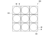
- One of the requirements for MEMS optical switch devices is that as many mirrors as possible be densely arranged inside the device.
- the MEMS optical switch device is equipped with a mirror array in which multiple mirrors are arranged.
- the mirror array is composed, for example, of multiple electrostatically driven mirror devices called MEMS mirrors mounted on a support substrate.
- the electrostatically driven mirror device is, for example, a silicon chip on which the mirrors and the comb-tooth electrodes that drive them are formed, and is manufactured by processing with submicron-level precision using techniques such as photolithography and etching.
- the top surface of a conventional electrostatically driven mirror device must also be equipped with peripheral circuits such as comb-shaped electrodes that drive the mirror and wiring to supply power to the comb-shaped electrodes.
- peripheral circuits such as comb-shaped electrodes that drive the mirror and wiring to supply power to the comb-shaped electrodes.
- conventional electrostatically driven mirror devices have been forced to limit the size of the mirror to some extent in order to secure space for arranging these peripheral circuits.
- the external terminals of the device must be connected to the external wiring by wire bonding or the like. In that case, it is necessary to provide space between the electrostatically driven mirror devices in order to install the external wiring.
- the present invention has been made in consideration of the above circumstances, and aims to provide a mirror device, a mirror array, and a MEMS-type optical switch device that have large mirrors that can be arranged adjacent to each other on a supporting substrate.
- the present invention employs the following configuration.
- a housing having a cavity A mirror disposed on one side of the housing; A functional layer disposed on the other surface side of the housing; an operation unit disposed in the hollow portion of the housing and connecting the functional layer and the mirror; A mirror device, wherein the functional layer includes a first electrostatic actuator that rotates the mirror in a first rotation direction, a second electrostatic actuator that rotates the mirror in a second rotation direction intersecting the first rotation direction, and a terminal portion arranged on the surface opposite the housing.
- the functional layer includes a first electrostatic actuator that rotates the mirror in a first rotation direction, and a second electrostatic actuator that rotates the mirror in a second rotation direction that intersects with the first rotation direction, a mirror device, wherein the first actuator and the second actuator each have a first comb-shaped electrode made of the first semiconductor layer, and a second comb-shaped electrode made of the first semiconductor layer, the interlayer insulating layer, and the second semiconductor layer.
- the functional layer includes a first semiconductor layer, a second semiconductor layer, and an interlayer insulating layer disposed between the first semiconductor layer and the second semiconductor layer,
- the mirror device described in [1] wherein the first actuator and the second actuator each have a first comb-shaped electrode made of the first semiconductor layer, and a second comb-shaped electrode made of the first semiconductor layer, the interlayer insulating layer, and the second semiconductor layer.
- the functional layer includes: A first movable portion to which the operation portion is joined; A ring-shaped second movable portion arranged to surround the first movable portion; a fixed portion disposed so as to surround the second movable portion and joined to the other surface side of the housing; a wiring portion adjacent to the second movable portion and joined to the other surface side of the housing; A plurality of the terminal portions disposed on the fixed portion and the wiring portion; a first torsion beam portion extending in a rotation axis direction in the first rotation direction and connecting the first movable portion and the second movable portion; a second torsion beam portion extending in a rotation axis direction in the second rotation direction and connecting the second movable portion and the wiring portion; is provided, the first movable portion, the second movable portion, the fixed portion, the wiring portion, and the second torsion beam portion are composed of the first semiconductor layer, and the interlayer insulating layer and the second semiconductor layer that cover at least a part or all of the first semiconductor layer,
- the functional layer includes: A first movable part that directly or indirectly fixes the mirror; A ring-shaped second movable portion arranged to surround the first movable portion; a fixed portion disposed so as to surround the second movable portion and joined to the other surface side of the housing; a wiring portion adjacent to the second movable portion and joined to the other surface side of the housing; A plurality of terminal portions disposed on the fixed portion and the wiring portion; a first torsion beam portion extending in a rotation axis direction in the first rotation direction and connecting the first movable portion and the second movable portion; a second torsion beam portion extending in a rotation axis direction in the second rotation direction and connecting the second movable portion and the wiring portion; is provided, the first movable portion, the second movable portion, the fixed portion, the wiring portion, and the second torsion beam portion are composed of the first semiconductor layer, and the interlayer insulating layer and the second semiconductor layer that cover at least a part or all of the first semiconductor layer,
- the first comb electrode of the first actuator is provided on the first movable part, and the second comb electrode is provided on the second movable part,
- the fixed portion is divided into a plurality of divided regions, the second comb-shaped electrode of the second actuator is provided in each of the divided regions, Each of the divided regions is provided with a first via penetrating the interlayer insulating layer to electrically connect the first semiconductor layer and the second semiconductor layer that constitute the divided region, and a first terminal portion that is on the second semiconductor layer and connected to the first via;
- the mirror device described in [6] wherein the first terminal portion is electrically connected to a second semiconductor layer constituting the second comb-like electrode of the second actuator, and is electrically connected to a first semiconductor layer constituting the second comb-like electrode of the second actuator via the first via.
- the second comb electrode constituting the first actuator is provided on an inner side of the annular second movable part, and the first comb electrode constituting the second actuator is provided on an outer side of the annular second movable part, the first semiconductor layer of the second movable portion is provided with a buried insulating layer that insulates and separates the second comb-shaped electrode of the first actuator on an inner side from the first comb-shaped electrode of the second actuator on an outer side,
- the second semiconductor layer of the second torsion beam portion is connected to a second terminal portion provided on the wiring portion, the first semiconductor layer of the second torsion beam portion is connected to a third terminal portion provided on the wiring portion, the second terminal portion is electrically connected to the first semiconductor layer and the second semiconductor layer constituting the second comb
- the annular second movable portion is provided on an inner side thereof with the second comb-like electrode constituting the first actuator, and is provided on an outer side thereof with the first comb-like electrode constituting the second actuator, the second semiconductor layer of the second torsion beam portion is connected to a second terminal portion provided on the wiring portion, the first semiconductor layer of the second torsion beam portion is connected to a third terminal portion provided on the wiring portion, the second terminal portion is electrically connected to the second semiconductor layer constituting the second comb-shaped electrode of the first actuator via the second semiconductor layer constituting the second torsion beam portion, the third terminal portion is electrically connected to the first semiconductor layer constituting the first comb-like electrode of the second actuator and the first semiconductor layer constituting the second comb-like electrode of the first actuator via the first semiconductor layer of the second torsion beam portion,
- the fixed portion is divided into a plurality of divided regions, the second comb-shaped electrode of the second actuator is provided in each of the divided regions,
- the second semiconductor layer is divided into two regions, one region of the second semiconductor layer, together with the first semiconductor layer, constitutes the second comb electrode of the second actuator;
- the other region of the second semiconductor layer is provided with a first via penetrating the interlayer insulating layer to electrically connect the second semiconductor layer and the first semiconductor layer constituting the other region, and a first terminal portion located on the other region of the second semiconductor layer and connected to the first via;
- the mirror device according to [6] wherein the first terminal portion is electrically connected to a first semiconductor layer constituting the second comb-shaped electrode of the second actuator through the first via.
- the second comb electrode constituting the first actuator is provided on an inner side of the annular second movable part, and the first comb electrode constituting the second actuator is provided on an outer side of the annular second movable part, the first semiconductor layer of the second movable portion is provided with a buried insulating layer that insulates and separates the second comb-shaped electrode of the first actuator on an inner side from the first comb-shaped electrode of the second actuator on an outer side,
- the mirror device described in [11] further comprises a second via penetrating the interlayer insulating layer to electrically connect the second semiconductor layer to the first semiconductor layer of the second comb-tooth electrode of the first actuator on the inside.
- the second semiconductor layer of the second torsion beam portion is electrically connected to a second terminal portion provided on the wiring portion, the first semiconductor layer of the second torsion beam portion is connected to a third terminal portion provided on the wiring portion, the second terminal portion is electrically connected to the first semiconductor layer and the second semiconductor layer constituting the second comb-shaped electrode of the first actuator via the second semiconductor layer constituting the second torsion beam portion and the second via of the second movable portion, the third terminal portion is electrically connected to the first semiconductor layer constituting the first comb-shaped electrode of the second actuator via the first semiconductor layer of the second torsion beam portion,
- a plurality of mirror devices are provided on a supporting substrate, A mirror array, wherein the mirror device is the mirror device according to any one of [1] to [5] or [7] to [13].
- a plurality of mirror devices are provided on a supporting substrate, A mirror array, wherein the mirror device is the mirror device according to [6].
- the mirror array according to [14] wherein the mirror device is bonded to a supporting substrate via a bump formed on the terminal portion.
- the mirror array according to [15], wherein the mirror device is bonded to a supporting substrate via a bump formed on the terminal portion.
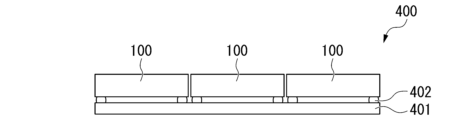
- the mirror array according to [14] wherein the distance between the mirror devices is 0.5 mm or less.
- a MEMS type optical switch device for optical fibers having a mirror array the mirror array having a plurality of mirror devices on a supporting substrate, the mirror devices being the mirror devices according to any one of [1] to [5] or [7] to [13].
- a MEMS type optical switch device for optical fibers having a mirror array the mirror array having a plurality of mirror devices on a supporting substrate, the mirror devices being the mirror device according to [6].
- a mirror is arranged on one side of a housing, and a functional layer including a first actuator and the second actuator is arranged on the other side of the housing. Therefore, the size of the mirror is not restricted by the installation area of the actuator, and a large-area mirror can be provided.
- the terminal portion is arranged on the surface of the functional layer opposite the housing, for example, when constructing a mirror array, the wiring on the supporting substrate side can be arranged directly below the mirror device. As a result, when arranging multiple mirror devices on a supporting substrate, etc., there is no need to provide wiring space on the supporting substrate between the mirror devices, and the mirror devices can be arranged closely together.
- the functional layer that drives the mirror has a first semiconductor layer, a second semiconductor layer, and an interlayer insulating layer, and is provided with a first actuator and a second actuator, and the first actuator and the second actuator each have a first comb-shaped electrode and a second comb-shaped electrode, respectively, so that the actuator can be made thinner and the structure of the actuator can be simplified.
- the orientation of the mirror can be freely changed by the first actuator and the second actuator.
- the functional layer has a first semiconductor layer, a second semiconductor layer, and an interlayer insulating layer, and the first and second comb-shaped electrodes of the first and second actuators are composed of these layers, making it possible to reduce the thickness of the actuators and simplify the structure of the actuators.
- the first movable part is attached to the second movable part via the first torsion beam part, and the second movable part is attached to the wiring part via the second torsion beam part. Therefore, the first movable part can be rotated in a first rotation direction and a second rotation direction, and the orientation of the mirror connected to the first movable part via the operating part can be freely changed.
- the first actuator is composed of a first comb-shaped electrode provided on the first movable part and a second comb-shaped electrode provided on the second movable part
- the first movable part can be rotated in a first rotation direction relative to the second movable part
- the second actuator is composed of a first comb-shaped electrode provided on the second movable part and a second comb-shaped electrode provided on the fixed part
- the second movable part can be rotated in a second rotation direction relative to the fixed part and the wiring part.
- first movable part to be rotated in the first rotation direction and the second rotation direction relative to the housing, and since the rotation amount in the first rotation direction and the second rotation direction can be changed individually by the first actuator and the second actuator, the orientation of the mirror connected to the first movable part can be freely changed.
- the fixed portion is divided into a plurality of divided regions, and a second comb-shaped electrode of the second actuator is provided in each divided region.
- Each divided region is further provided with a first via that electrically connects the first semiconductor layer and the second semiconductor layer that constitute the second comb-shaped electrode of the second actuator, and a first terminal portion.
- the first terminal portion is electrically connected to the first semiconductor layer and the second semiconductor layer that constitute the second comb-shaped electrode of the second actuator, so that a voltage for operating the second actuator can be applied from the first terminal portion arranged on the upper surface side of the functional layer.
- the first semiconductor layer of the second movable part is provided with a buried insulating layer that insulates and separates the second comb-shaped electrode of the first actuator from the first comb-shaped electrode of the second actuator, and is provided with a second via that connects the second semiconductor layer to the first semiconductor layer of the second comb-shaped electrode of the first actuator.
- the second terminal portion provided on the wiring portion is electrically connected to the first semiconductor layer and the second semiconductor layer that constitute the second comb-shaped electrode of the first actuator
- the third terminal portion provided on the wiring portion is electrically connected to the first semiconductor layer that constitutes the first comb-shaped electrode of the second actuator
- the third terminal portion is further electrically connected to the first semiconductor layer that constitutes the first comb-shaped electrode of the first actuator. Therefore, a voltage for operating the first actuator and the second actuator can be applied from the second terminal portion and the third terminal portion arranged on the upper surface side of the functional layer.
- the second terminal portion provided on the wiring portion is electrically connected to the second semiconductor layer constituting the second comb-shaped electrode of the first actuator
- the third terminal portion provided on the wiring portion is electrically connected to the first semiconductor layer constituting the first comb-shaped electrode of the second actuator and the first semiconductor layer constituting the second comb-shaped electrode of the first actuator
- the third terminal portion is further electrically connected to the first semiconductor layer constituting the first comb-shaped electrode of the first actuator. Therefore, a voltage for operating the first actuator and the second actuator can be applied from the second terminal portion and the third terminal portion arranged on the upper surface side of the functional layer.
- the fixed portion is divided into a plurality of divided regions, and a second comb-shaped electrode of the second actuator is provided in each divided region.
- the second semiconductor layer is divided into two regions, and one region of the divided second semiconductor layer constitutes the second comb-shaped electrode of the second actuator together with the first semiconductor layer.
- the other region of the second semiconductor layer is provided with a first via that electrically connects the second semiconductor layer and the first semiconductor layer that constitute the divided region, and a first terminal portion.
- the first terminal portion is electrically connected to the first semiconductor layer that constitutes the second comb-shaped electrode of the second actuator, so that a voltage for operating the second actuator can be applied from the first terminal portion arranged on the upper surface side of the functional layer.
- the first semiconductor layer of the second movable part is provided with a buried insulating layer that insulates and separates the second comb-shaped electrode of the first actuator from the first comb-shaped electrode of the second actuator, and a second via is provided that electrically connects the second semiconductor layer of the second movable part to the first semiconductor layer of the second comb-shaped electrode of the first actuator. Therefore, the first semiconductor layer constituting the second comb-shaped electrode of the first actuator and the first semiconductor layer constituting the first comb-shaped electrode of the second actuator, both formed in the second movable part, can be electrically separated, and the first actuator and the second actuator can be controlled individually.
- the second terminal portion provided on the wiring portion is electrically connected to the second semiconductor layer and the first semiconductor layer that constitute the second comb-shaped electrode of the first actuator
- the third terminal portion provided on the wiring portion is electrically connected to the first semiconductor layer that constitutes the first comb-shaped electrode of the second actuator
- the third terminal portion is further electrically connected to the first semiconductor layer that constitutes the first comb-shaped electrode of the first actuator. Therefore, a voltage for operating the first actuator and the second actuator can be applied from the second terminal portion and the third terminal portion arranged on the upper surface side of the functional layer.
- the mirror array described in the above [14] or [15] a plurality of mirrors can be arranged closely together.
- the mirror array described in [16] or [17] above since the mirror array is bonded to the supporting substrate via the bumps formed on the terminal portions, it is possible to reduce the wiring space on the supporting substrate.
- the distance between the mirror devices is 0.5 mm or less, so that the gap between the mirrors can be made small.
- the MEMS optical switch device described in [20] or [21] above since it is provided with a mirror array that allows a plurality of mirrors to be densely arranged, it is possible to realize a high-density and large-scale optical fiber changeover switch.
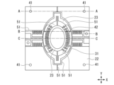
- FIG. 1A is a schematic plan view of a mirror device according to a first embodiment of the present invention.
- FIG. 1B is a schematic plan view showing a second semiconductor layer that constitutes the mirror device.
- FIG. 1C is a schematic plan view showing a first semiconductor layer that constitutes the mirror device.
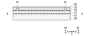
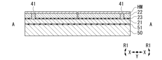
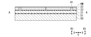
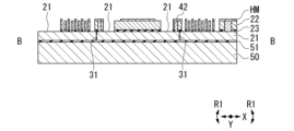
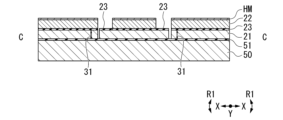
- FIG. 2 is a schematic cross-sectional view corresponding to line AA in FIG. 1A.
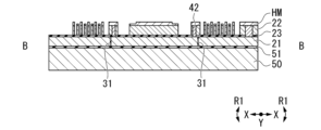
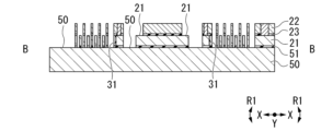
- FIG. 3 is a schematic cross-sectional view corresponding to line BB in FIG. 1A.
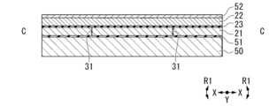
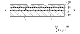
- FIG. 4 is a schematic cross-sectional view corresponding to line CC in FIG. 1A.
- 5 is an enlarged cross-sectional view of the buried insulating layer shown in FIG. 3.
- FIG. 6 is an enlarged cross-sectional view of the buried insulating layer shown in FIG.
- FIG. 7 is a schematic plan view of a mirror device according to a first embodiment of the present invention.
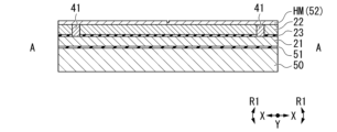
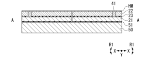
- FIG. 8 is a schematic cross-sectional view corresponding to line DD in FIG.
- FIG. 9 is a diagram for explaining the operation of the mirror device according to the first embodiment of the present invention, and is a schematic cross-sectional view corresponding to line CC in FIG. 1A.
- FIG. 10A is a schematic plan view illustrating a manufacturing method for a mirror device according to the first embodiment of the present invention.
- FIG. 10-2 is a schematic cross-sectional view corresponding to line AA in FIG. 10-1.
- FIG. 10-3 is a schematic cross-sectional view corresponding to line BB in FIG. 10-1.
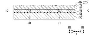
- FIG. 10-4 is a schematic cross-sectional view corresponding to line CC in FIG. 10-1.
- FIG. 11A is a schematic plan view illustrating a manufacturing method for a mirror device according to the first embodiment of the present invention.
- FIG. 11-2 is a schematic cross-sectional view corresponding to line AA in FIG. 11-1.
- FIG. 11-3 is a schematic cross-sectional view corresponding to line BB in FIG. 11-1.
- FIG. 11-4 is a schematic cross-sectional view corresponding to line CC in FIG. 11-1.
- FIG. 12A is a schematic plan view illustrating a manufacturing method for a mirror device according to the first embodiment of the present invention.
- FIG. 12-2 is a schematic cross-sectional view corresponding to line AA in FIG. 12-1.
- FIG. 12-3 is a schematic cross-sectional view corresponding to line BB in FIG. 12-1.
- FIG. 12-4 is a schematic cross-sectional view corresponding to line CC in FIG. 12-1.
- FIG. 13A is a schematic plan view illustrating a manufacturing method for a mirror device according to the first embodiment of the present invention.
- FIG. 13-2 is a schematic cross-sectional view corresponding to line AA in FIG. 13-1.
- FIG. 13-3 is a schematic cross-sectional view corresponding to line BB in FIG. 13-1.
- FIG. 13-4 is a schematic cross-sectional view corresponding to line CC in FIG. 13-1.
- FIG. 14A is a schematic plan view illustrating a manufacturing method for a mirror device according to the first embodiment of the present invention.
- FIG. 14A is a schematic plan view illustrating a manufacturing method for a mirror device according to the first embodiment of the present invention.
- FIG. 14-2 is a schematic cross-sectional view corresponding to line AA in FIG. 14-1.
- FIG. 14-3 is a schematic cross-sectional view corresponding to line BB in FIG. 14-1.
- FIG. 14-4 is a schematic cross-sectional view corresponding to line CC in FIG. 14-1.
- FIG. 15A is a schematic plan view illustrating a manufacturing method for a mirror device according to the first embodiment of the present invention.
- FIG. 15-2 is a schematic cross-sectional view corresponding to line AA in FIG. 15-1.
- FIG. 15-3 is a schematic cross-sectional view corresponding to line BB in FIG. 15-1.
- FIG. 15-4 is a schematic cross-sectional view corresponding to line CC in FIG. 15-1.
- FIG. 15A is a schematic plan view illustrating a manufacturing method for a mirror device according to the first embodiment of the present invention.
- FIG. 15-2 is a schematic cross-sectional view corresponding to line AA in FIG. 15-1.
- FIG. 16A is a schematic plan view illustrating a manufacturing method for a mirror device according to the first embodiment of the present invention.
- FIG. 16-2 is a schematic cross-sectional view corresponding to line AA in FIG. 16-1.
- FIG. 16-3 is a schematic cross-sectional view corresponding to line BB in FIG. 16-1.
- FIG. 16-4 is a schematic cross-sectional view corresponding to line CC in FIG. 16-1.
- FIG. 17A is a schematic plan view illustrating a manufacturing method for a mirror device according to the first embodiment of the present invention.
- FIG. 17-2 is a schematic cross-sectional view corresponding to line AA in FIG. 17-1.
- FIG. 17-3 is a schematic cross-sectional view corresponding to line BB in FIG. 17-1.
- FIG. 17-4 is a schematic cross-sectional view corresponding to line CC in FIG. 17-1.
- FIG. 18 is a schematic plan view of a mirror device according to a second embodiment of the present invention.
- FIG. 19 is a schematic plan view of a mirror device according to a third embodiment of the present invention.
- FIG. 20 is a schematic side view of a mirror array according to the fourth embodiment of the present invention.
- FIG. 21 is a schematic plan view of a mirror array according to a fourth embodiment of the present invention.
- the mirror device 100 of this embodiment includes at least a housing K, a mirror M, and a functional layer 1 disposed on the housing K to drive the mirror M. More specifically, the mirror device 100 of this embodiment includes a housing K having a cavity K1, a mirror M disposed on one surface K2 of the housing K, a functional layer 1 disposed on the other surface K3 of the housing K, and an operation unit K4 disposed in the cavity K1 of the housing K to connect the functional layer 1 and the mirror M.
- the housing K and the operation unit K4 are made of single crystal silicon and are, for example, cut out from a single crystal silicon substrate.
- the mirror M arranged on one surface K2 of the housing K has a reflecting surface M1 on the side opposite to the side on which the housing K is arranged.
- the functional layer 1 includes a first electrostatic actuator 2 that rotates the mirror M in a first rotation direction R1, a second electrostatic actuator 3 that rotates the mirror M in a second rotation direction R2 that intersects with the first rotation direction R1, and terminals T1 to T3 that are located on the surface 1A opposite the housing K.
- the first rotation direction R1 is a rotation direction with the Y direction as the rotation axis, as shown in Figures 2 to 4
- the second rotation direction R2 is a rotation direction with the X direction as the rotation axis, as shown in Figure 8.
- the X direction and the Y direction are perpendicular to each other on the same plane.
- the functional layer 1 is a multi-layer structure and includes a first semiconductor layer 21, a second semiconductor layer 22, and an interlayer insulating layer 23 disposed between the first semiconductor layer 21 and the second semiconductor layer 22.
- the first semiconductor layer 21 and the second semiconductor layer 22 are made of, for example, silicon layers, and the interlayer insulating layer 23 is made of, for example, a silicon oxide layer.
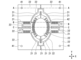
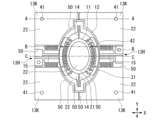
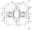
- the functional layer 1 is formed with a first movable portion 11, a second movable portion 12, a fixed portion 13K, a wiring portion 13H, a plurality of terminal portions T1, T2, and T3, a first torsion beam portion 14, and a second torsion beam portion 15.
- Figures 1B and 1C show schematic plan views of the second semiconductor layer 22 and the first semiconductor layer 21.
- the first movable portion 11, the second movable portion 12, the fixed portion 13K, the wiring portion 13H, the multiple terminal portions T1, T2, T3, the first torsion beam portion 14, and the second torsion beam portion 15 are formed in the functional layer 1 by processing the first semiconductor layer 21, the second semiconductor layer 22, and the interlayer insulating layer 23 into desired shapes using microfabrication techniques including photolithography. That is, the first movable portion 11, the second movable portion 12, the fixed portion 13K, the wiring portion 13H, and the second torsion beam portion 15 are composed of the first semiconductor layer 21, and the interlayer insulating layer 23 and the second semiconductor layer 22 that cover at least a part or all of the first semiconductor layer 21.
- the first torsion beam portion 14 is also composed of the first semiconductor layer 21.
- the functional layer 1 includes two first actuators 2 (2A, 2B) and four second actuators 3 (3A to 3D).
- the first actuators 2A, 2B and the second actuators 3A to 3D each have a first comb-shaped electrode D1 made of a first semiconductor layer 21 and a second comb-shaped electrode D2 made of the first semiconductor layer 21, an interlayer insulating layer 23 and a second semiconductor layer 22.
- the first actuators 2A, 2B and the second actuators 3A to 3D are formed together with the first movable portion 11, the second movable portion 12, the fixed portion 13K and the wiring portion 13H by microfabrication techniques including photolithography.
- the first actuators 2A and 2B are symmetrically positioned with respect to each other with respect to the first torsion beam portion 14, and the second actuators 3A, 3B and 3C, 3D are symmetrically positioned with respect to each other with respect to the second torsion beam portion 15.
- the following describes the functional layer 1, in particular the relationship between the first movable part 11, the second movable part 12, and the fixed part 13K and the first actuators 2A, 2B, and the second actuators 3A to 3D, and the relationship between the first comb-shaped electrode D1 and the second comb-shaped electrode D2 constituting each of the actuators 2A, 2B, 3A to 3D, and the first semiconductor layer 21, the interlayer insulating layer 23, and the second semiconductor layer 22.
- the first movable part 11 is located almost in the center of the functional layer 1, and the operation part K4 is joined to this first movable part 11.
- the mirror M is joined to the operation part K4.
- the first movable part 11 is a laminate of the first semiconductor layer 21, the interlayer insulating layer 23, and the second semiconductor layer 22, but in a part of the first movable part 11, the interlayer insulating layer 23 and the second semiconductor layer 22 are not laminated, and the first movable part 11 is composed only of the first semiconductor layer 21.
- the first comb-shaped electrode D1 (D11) constituting the first actuator 2 is provided in the part composed only of the first semiconductor layer 21, the first comb-shaped electrode D1 (D11) constituting the first actuator 2 is provided.
- the first comb-shaped electrode D11 in the first movable part 11 is arranged on both sides of the first movable part 11 in the X direction.
- the first comb-shaped electrode D11 protrudes in the X direction.
- the second movable part 12 is a ring-shaped member arranged to surround the first movable part 11.
- the second movable part 12 has a ring-shaped part 12A and four electrode parts 12B that protrude outward from the ring-shaped part 12A.
- the ring-shaped part 12A is made of a laminate of a first semiconductor layer 21, an interlayer insulating layer 23, and a second semiconductor layer 22, and is joined to the second torsion beam part 15.
- the electrode parts 12B are made of only the first semiconductor layer 21, and protrude from the ring-shaped part 12A.
- the first semiconductor layer 21 of the ring-shaped part 12A and the first semiconductor layer 21 of the electrode parts 12B are a continuous layer.
- second comb-like electrodes D2 constituting two sets of first actuators 2A, 2B are provided. These second comb-like electrodes D21 are arranged so as to face the two first comb-like electrodes D11 provided on the first movable portion 11, respectively.
- the second comb-like electrodes D21 are composed of a laminate of a first semiconductor layer 21, an interlayer insulating layer 23, and a second semiconductor layer 22.
- the four electrode portions 12B of the second movable portion 12 are provided with the first comb-like electrodes D1 (D31) of the second actuators 3A to 3D.
- the first comb-like electrodes D31 are made only of the first semiconductor layer 21.
- the first comb-like electrodes D31 in the second movable portion 12 are provided so as to protrude from the electrode portions 12B in the Y direction.
- the first semiconductor layer 21 of the annular portion 12A is provided with a buried insulating layer 31.
- the buried insulating layer 31 is provided to divide the first semiconductor layer 21 into two regions.
- the buried insulating layer 31 is an insulating layer for electrically insulating and isolating the first semiconductor layer 21 constituting the second comb-shaped electrodes D21 of the first actuators 2A and 2B located inside the annular portion 12A from the first semiconductor layer 21 constituting the first comb-shaped electrodes D31 of the second actuators 3A to 3D located in the electrode portion 12B on the outside of the annular portion 12A.
- FIG. 5 and 6 show enlarged cross-sectional views of the buried insulating layer 31.
- FIG. 5 is an enlarged cross-sectional view of the buried insulating layer 31 in FIG. 3.
- FIG. 6 is an enlarged cross-sectional view of the buried insulating layer 31 in FIG. 4.
- the buried insulating layer 31 is formed by forming a wall surface insulating layer 32b and a filling layer 31c inside a trench groove 31a provided in the first semiconductor layer 21.
- the wall surface insulating layer 32b is made of, for example, silicon nitride
- the filling layer 31c is made of, for example, polysilicon.
- the buried insulating layer 31 thus formed surrounds a part of the inner periphery of the annular portion 12A, as shown in FIG. 1A.
- the second comb-shaped electrode D21 of the first actuator 2A, 2B and the second via 42 are arranged in the area surrounded by the buried insulating layer 31.
- the second movable portion 12 is provided with a second via 42 penetrating the second semiconductor layer 22 and the interlayer insulating layer 23.
- the second via 42 is provided to electrically connect the second semiconductor layer 22 of the second movable portion 12 to the first semiconductor layer 21. More specifically, the second via 42 is provided at a position within the region divided by the embedded insulating layer 31 where it is possible to electrically connect the first semiconductor layer 21 constituting the second comb-shaped electrode D21 of the first actuators 2A and 2B to the second semiconductor layer 22.
- the second via 42 is made of, for example, polycrystalline silicon or metal.
- the fixed portion 13K is disposed so as to surround the second movable portion 12, and is joined to the other surface K3 of the housing K.
- the entire functional layer 1 is disposed on the other surface K3 of the housing K.
- the fixed portion 13K is composed of a laminate in which a first semiconductor layer 21, a second semiconductor layer 22, and an interlayer insulating layer 23 are stacked.
- the fixed portion 13K is divided into four divided regions 13A to 13D. That is, as shown in FIG. 1A and FIG.
- the divided regions 13A to 13D are insulated and separated from each other because the first semiconductor layer 21, the second semiconductor layer 22, and the interlayer insulating layer 23 are not continuous between adjacent divided regions, and a lower insulating layer 51 is disposed between the housing K and the first semiconductor layer 21. Additionally, each of the divided regions 13A to 13D of the fixed portion 13K is also insulated and separated from the wiring portion 13H.
- the second comb-like electrodes D2 (D41) of the second actuators 3A to 3D are provided in each divided region 13A to 13D of the fixed portion 13K.
- the second comb-like electrodes D41 are composed of a laminate of a first semiconductor layer 21, an interlayer insulating layer 23, and a second semiconductor layer 22.
- the second comb-like electrodes D41 in the fixed portion 13K protrude in the Y direction, and thus face the first comb-like electrodes D31 provided in the electrode portion 12B of the second movable portion 12.
- the split regions 13A to 13D of the fixed portion 13K are each provided with a first via 41 penetrating the second semiconductor layer 22 and the interlayer insulating layer 23.
- the first via 41 electrically connects the first semiconductor layer 21 constituting the second comb-shaped electrode D41 of the second actuator 3A to 3D to the second semiconductor layer 22 constituting each split region 13A to 13D.
- the first via 41 is exposed on the surface of the second semiconductor layer 22, and the surface of this first via 41 is used as the first terminal portion T1.
- the first terminal portion T1 is located on the first via 41 and is on the same plane as the surface of the second semiconductor layer 22.
- the first via 41 is made of, for example, polycrystalline silicon or metal.
- the first terminal portion T1 is electrically connected to the second semiconductor layer 22 constituting the second comb-shaped electrode D2 (D41) of the second actuator 3A to 3D, and is electrically connected to the first semiconductor layer 21 constituting the second comb-shaped electrode D2 (D41) of the second actuator 3A to 3D through the first via 41.
- the wiring portion 13H is disposed in a position surrounding the second movable portion 12, similar to the fixed portion 13K, and is particularly adjacent to the second movable portion 12.
- the functional layer 1 is disposed on the other surface K3 side of the housing K.
- the wiring portion 13H is composed of a laminate made of a first semiconductor layer 21, an interlayer insulating layer 23 laminated on a portion of the first semiconductor layer 21, and a second semiconductor layer 22.
- the second semiconductor layer 22 constituting the wiring portion 13H is divided into two regions, and the second terminal portion T2 is provided in one of the regions.
- the second terminal portion T2 is electrically insulated from the first semiconductor layer 21 of the wiring portion 13H by the interlayer insulating layer 23.
- a third via 43 is formed in the other region of the divided second semiconductor layer, and a third terminal portion T3 is provided on the third via 43 and the second semiconductor layer 22.
- the third via 43 penetrates the interlayer insulating layer 23 to electrically connect the first semiconductor layer 21 and the second semiconductor layer 22.
- the third terminal portion T3 is electrically connected to the first semiconductor layer 21 of the wiring portion 13H, while being electrically isolated from the second terminal portion T2.
- the second torsion beam portion 15 is a member that connects the second movable portion 12 and the wiring portion 13H, and extends in the rotation axis direction (x direction) of the second rotation direction R2.
- the second torsion beam portion 15 is composed of a laminate of a first semiconductor layer 21, a second semiconductor layer 22, and an interlayer insulating layer 23.
- One end of the second torsion beam portion 15 is connected to the wiring portion 13H.
- the second terminal portion T2 is electrically connected to the second semiconductor layer 22 of the second torsion beam portion 15, and the third terminal portion T3 is electrically connected to the first semiconductor layer 21 of the second torsion beam portion 15.
- the other end of the second torsion beam portion 15 is connected to the second movable portion 12 as described above.
- the first torsion beam portion 14 is a member that connects the first movable portion 11 and the second movable portion 12, and extends in the rotation axis direction (Y direction) of the first rotation direction R1.
- the first torsion beam portion 14 is composed only of the first semiconductor layer 21.
- the second terminal portion T2 is electrically connected to the first semiconductor layer 21 and the second semiconductor layer 22 that constitute the second comb-shaped electrode D2 (D21) of the first actuator 2A, 2B via the second semiconductor layer 22 that constitutes the second torsion beam portion 15, the second semiconductor layer 22 of the second movable portion, and the second via 42.
- the third terminal portion T3 is electrically connected via the first semiconductor layer 21 of the second torsion beam portion 15 to the first semiconductor layer 21 constituting the first comb-shaped electrode D1 (D31) of the second actuator. Furthermore, the third terminal portion T3 is electrically connected to the first semiconductor layer 21 constituting the first comb-tooth electrode D1 (D11) of the first actuator 2A, 2B via the first semiconductor layer 21 of each of the second torsion beam portion 15, the second movable portion 12, and the first torsion beam portion 14.
- the first actuators 2A to 2B are configured by arranging a first comb-like electrode D11 provided on the first movable portion 11 and a second comb-like electrode D21 provided on the second movable portion 12 so as to face each other.
- the second actuators 3A to 3D are configured by arranging a first comb-like electrode D31 provided on the second movable portion 12 and a second comb-like electrode D41 provided on the fixed portion 13K so as to face each other.
- the first comb-like electrodes D11 and D31 of each of the actuators 2A, 2B, 3A to 3D are made of only the first semiconductor layer 21, and the second comb-like electrodes D21 and D41 of each of the actuators 2A, 2B, 3A to 3D are made of the first semiconductor layer 21, the second semiconductor layer 22, and the interlayer insulating layer 23.
- the first comb-like electrodes D11, D31 and the second comb-like electrodes D21, D41 are located at approximately the same height in the thickness direction of the functional layer 1. However, the thickness of the second comb-like electrodes D21, D41 is greater than that of the first comb-like electrodes D11, D31.
- first movable part 11 When the first movable part 11 is rotated in the first rotation direction R1 by the first actuators 2A and 2B, a height displacement occurs between the first movable part 11 and the second movable part 12 in one of the first actuators 2A and 2B.
- the first comb-shaped electrode D11 of the first actuator 2A on the right side of FIG. 2 is displaced upward in FIG. 2. This causes the entire first movable part 11 to tilt, and since the first actuators 2A and 2B are located symmetrically with respect to the first torsion beam part 14, a twist occurs in the first torsion beam part 14 connecting the first movable part 11 and the second movable part 12.
- FIG. 9 shows the state in which the first movable part 11 is rotated in the first rotation direction R1 relative to the second movable part 12 by the first actuator 2A (right side). To obtain rotation in the opposite direction, the first actuator 2B (left side) is driven.
- the second movable part 12 when the second movable part 12 is rotated in the second rotation direction R2 by the second actuators 3A to 3D, a height displacement is generated between the second movable part 12 and the fixed part 13K in either the pair of second actuators 3A and 3C or the pair of second actuators 3B and 3D among the second actuators 3A to 3D.
- the first comb-shaped electrodes D31 of the two second actuators 3A and 3C on the upper side of FIG. 1A are displaced toward the front of the paper in FIG. 1A.
- the second actuators 3B and 3D are used.
- the second movable part 12 is tilted, and since the second actuators 3A to 3D are located symmetrically with respect to the second torsion beam part 15, a twist is generated in the second torsion beam part 15 connecting the second movable part 12 and the wiring part 13H. In this way, the second actuators 3A to 3D make it possible to rotate the second movable part 12 in the second rotation direction R2 relative to the fixed part 13K.
- the first actuators 2A, 2B can rotate the first movable part 11 in the first rotation direction R1 relative to the second movable part 12, and the second actuators 3A-3D can rotate the second movable part 12 in the second rotation direction R2 relative to the fixed part 13K and the wiring part 13H, so that the first movable part 11 can be rotated in the first rotation direction R1 and the second rotation direction R2.
- the first actuators 2A, 2B and the second actuators 3A-3D can change the amount of rotation in the first rotation direction R1 and the second rotation direction R2 individually, so that the orientation of the reflective surface M1 of the mirror M connected to the first movable part 11 can be freely changed relative to the housing K.
- a first driving voltage is applied to the second semiconductor layer 22 from the second terminal T2.
- the first driving voltage applied to the second semiconductor layer 22 from the second terminal T2 reaches the second semiconductor layer 22 of the second movable portion 12 via the second torsion beam portion 15, and is applied directly to the second semiconductor layer 22 constituting the second comb-shaped electrodes D21 of the first actuators 2A and 2B provided in the second movable portion 12.
- the first driving voltage that reaches the second semiconductor layer 22 of the second movable portion 12 is also applied to the first semiconductor layer 21 constituting the second comb-shaped electrodes D21 of the first actuators 2A and 2B via the second via 42.
- the first driving voltage is not applied to the first comb-shaped electrodes D31 of the second actuators 3A to 3D.
- a third drive voltage is applied to the third terminal T3.
- the third drive voltage is a voltage having a different voltage value from the first drive voltage, and may be a ground voltage.
- the third drive voltage applied from the third terminal T3 reaches the first semiconductor layer 21 of the second movable part 12 via the first semiconductor layer 21 of the second torsion beam part 15, and is applied to the first semiconductor layer 21 of the first movable part 11, i.e., the first comb-shaped electrode D1 (D11) of the first actuators 2A and 2B via the first torsion beam part 14. This displaces the first comb-shaped electrode D1 (D11) of the first actuator 2A or 2B.
- the third drive voltage is also applied to the first semiconductor layer 21 constituting the second comb-shaped electrode D41 of the second actuators 3A to 3D.
- the first actuators 2A and 2B can be operated by applying a first drive voltage to the second comb-shaped electrodes D21 of the first actuators 2A and 2B and applying a third drive voltage (e.g., ground voltage) to the first comb-shaped electrodes D11.
- a third drive voltage e.g., ground voltage
- a second drive voltage is applied from the first terminal T1 to the second semiconductor layer 22 of the fixed portion 13K.
- the second drive voltage may be a voltage having the same voltage value as the first drive voltage, or may be a voltage having a different voltage value.
- the second drive voltage is a voltage having a different voltage value from the third drive voltage.
- the second drive voltage applied from the first terminal T1 to the second semiconductor layer 22 is applied as is to the second semiconductor layer 22 constituting the second comb-shaped electrodes D41 of the second actuators 3A to 3D provided in the division regions 13A to 13D.
- the second drive voltage applied to the second semiconductor layer 22 is also applied to the first semiconductor layer 21 constituting the second comb-shaped electrodes D41 of the second actuators 3A to 3D via the first vias 41.
- the third drive voltage (e.g., ground voltage) applied to the third terminal T3 is also applied to the first semiconductor layer 21 constituting the first comb-shaped electrodes D31 of the second actuators 3A to 3D. This displaces the first comb-shaped electrodes D31 of the second actuators 3A to 3D.
- the second actuators 3A to 3D can be operated by applying the second drive voltage to the second comb-shaped electrodes D41 of the second actuators 3A to 3D and applying the third drive voltage (e.g., ground voltage) to the first comb-shaped electrodes D31.
- the third drive voltage e.g., ground voltage
- a substrate is prepared in which a support substrate 50, a lower insulating layer 51, and a first semiconductor layer 21 are laminated.
- This may be prepared by film formation, or an SOI substrate may be used.
- the support substrate 50 is, for example, a silicon substrate
- the lower insulating layer 51 is, for example, a silicon oxide layer
- the first semiconductor layer 21 is, for example, a silicon layer.
- the buried insulating layer 31 is formed in this first semiconductor layer 21.
- the buried insulating layer 31 is formed by forming a trench groove in the first semiconductor layer 21, then forming an insulating film that will become the wall surface insulating layer 32b on the first semiconductor layer 21 and in the trench groove, then forming a polysilicon layer that will become the filling layer 31c on the first semiconductor layer 21 and in the trench groove, and removing the insulating film and polysilicon layer stacked on the first semiconductor layer 21 to form the buried insulating layer 31 as shown in detail in Figures 5 and 6.
- an interlayer insulating layer 23 and a second semiconductor layer 22 are formed on the first semiconductor layer 21.
- the interlayer insulating layer 23 is, for example, a silicon oxide layer
- the second semiconductor layer is, for example, a silicon layer.
- the interlayer insulating layer 23 and the second semiconductor layer 22 may be formed by a normal film forming technique, or may be formed by bonding an SOI substrate.
- a first via 41 and a second via 42 are formed at a predetermined position of the second semiconductor layer 22.
- the first via 41 and the second via 42 are formed by forming a through hole penetrating the second semiconductor layer 22 and the interlayer insulating layer 23, and filling the through hole with, for example, polysilicon or metal.
- an upper insulating layer 52 is formed on the second semiconductor layer 22.
- the upper insulating layer 52 is, for example, made of a silicon oxide layer.
- This upper insulating layer 52 becomes a hard mask layer for forming each part of the functional layer 1.
- the upper insulating layer 52 may be referred to as a hard mask layer HM.
- the upper insulating layer 52 is partially etched to a depth of about 1/4 to 1/3 of its film thickness, thereby forming the upper insulating layer 52 into a hard mask layer HM having a cross-sectional shape as shown in Figures 12-2 to 12-4. Note that the illustration of the hard mask layer HM is omitted in Figure 12-1.
- the hard mask layer HM (upper insulating layer 52) is partially etched to a depth of about 1/4 to 1/3 of the original film thickness, so that the upper insulating layer 52 becomes a hard mask layer HM with a cross-sectional shape as shown in Figures 13-2 to 13-4.
- the hard mask layer HM is formed into a relatively thick portion and a relatively thin portion, and further, a portion where the hard mask layer HM does not exist is also formed.
- the relatively thick portion of the hard mask layer HM will ultimately be the portion where the first semiconductor layer 21, the second semiconductor layer 22, and the interlayer insulating layer 23 remain.
- the relatively thin portion of the hard mask layer HM will ultimately be the portion where the first semiconductor layer 21 remains and the second semiconductor layer 22 and the interlayer insulating layer 23 are removed. Furthermore, the portions where the hard mask layer HM does not exist will ultimately be portions where the first semiconductor layer 21, the second semiconductor layer 22, and the interlayer insulating layer 23 are all removed.
- the second semiconductor layer 22 is partially removed by etching using the hard mask layer HM as a mask.
- the portions from which the second semiconductor layer 22 is removed correspond to the portions in Figs. 13-1 to 13-4 where the hard mask layer HM is not present.
- the interlayer insulating layer 23 that is partially exposed by removing the second semiconductor layer 22 is removed by etching. At this time, part of the hard mask layer HM is also removed.
- the hard mask layer HM that remains at this stage corresponds to the relatively thick part in Figs. 13-1 to 13-4.
- the lower insulating layer 51 that is partially exposed by removing the first semiconductor layer 21 is removed by etching. At this time, all remaining parts of the hard mask layer HM are removed. At this stage, the first movable portion 11, the second movable portion 12, the fixed portion 13K, the wiring portion 13H, the first torsion beam portion 14, and the second torsion beam portion 15 of the functional layer 1 are formed.
- a cavity K1 and an operating portion K4 are formed by removing a portion of the single crystal silicon substrate 50. Then, the lower insulating layer 51 exposed by removing the portion of the single crystal silicon substrate 50 is removed to form the functional layer 1. Furthermore, a mirror M is attached to the operating portion K4. Through these steps, the mirror device 100 shown in Figures 1A to 8 is manufactured.
- the above describes one example of a method for manufacturing the mirror device 100.
- the mirror device 100 of this embodiment is not limited to being manufactured by the above manufacturing method.
- a mirror M is arranged on one surface K2 side of the housing K, and a functional layer 1 including the first actuators 2A, 2B and the second actuators 3A to 3D is arranged on the other surface K3 side of the housing K, so that the size of the mirror M is not restricted by the installation area of the actuators 2A to 3D, and a large-area mirror M can be provided. Furthermore, since multiple terminal portions (first terminal portion T1, second terminal portion T2, third terminal portion T3) are arranged on the surface of the functional layer 1 opposite the housing K, for example, when constructing a mirror array, the wiring on the supporting substrate side can be arranged directly below the mirror device 100. As a result, when arranging multiple mirror devices 100 on a supporting substrate, etc., there is no need to provide wiring space on the supporting substrate between the mirror devices 100, and the mirror devices 100 can be arranged closely together.
- the functional layer 1 has the first semiconductor layer 21, the second semiconductor layer 22, and the interlayer insulating layer 23, and the first comb-shaped electrode D1 and the second comb-shaped electrode D2 of the first actuators 2A, 2B and the second actuators 3A to 3D are composed of these layers 21 to 23, so that the actuators 2A to 3D can be made thinner and the structure of the actuators 2A to 3D can be simplified.
- the functional layer 1 that drives the mirror M has a first semiconductor layer 21, a second semiconductor layer 22 and an interlayer insulating layer 23, and is provided with first actuators 2A, 2B and second actuators 3A to 3D, and the first actuators 2A, 2B and the second actuators 3A to 3D each have a first comb-tooth electrode D1 and a second comb-tooth electrode D2, thereby making it possible to reduce the thickness of the actuators, reduce the thickness of the actuators 2A to 3D, and simplify the structure of the actuators 2A to 3D.
- the orientation of the mirror M can be freely changed by the first actuators 2A and 2B and the second actuators 3A to 3D.
- the first movable part 11 is attached to the second movable part 12 via the first torsion beam part 14, and the second movable part 12 is attached to the wiring part 13H via the second torsion beam part 15. Therefore, the first movable part 11 can be rotated in the first rotation direction R1 and the second rotation direction R2, and the orientation of the mirror M connected to the first movable part 11 via the operating part K4 can be freely changed.
- the first actuators 2A, 2B are composed of a first comb-tooth electrode D11 provided on the first movable part 11 and a second comb-tooth electrode D21 provided on the second movable part 12, so that the first movable part 11 can be rotated in a first rotation direction R1 relative to the second movable part 12.
- the second actuators 3A to 3D are composed of a first comb-tooth electrode D31 provided on the second movable part 12 and a second comb-tooth electrode D41 provided on the fixed part 13K, so that the second movable part 12 can be rotated in a second rotation direction R2 relative to the fixed part 13K and the wiring part 13H.
- first movable part 11 rotate in the first rotation direction R1 and the second rotation direction R2 relative to the housing K, and the amount of rotation in the first rotation direction R1 and the second rotation direction R2 can be changed individually by the first actuators 2A, 2B and the second actuators 3A-3D, so that the orientation of the mirror M connected to the first movable part 11 can be freely changed.
- the fixed portion 13K is divided into four divided regions 13A to 13D, and each divided region 13A to 13D is provided with a first via 41 that connects the first semiconductor layer 21 and the second semiconductor layer 22 that constitute the second comb-shaped electrode D41 of the second actuator 3A to 3D, and a first terminal portion T1, so that a voltage for operating the second actuator 3A to 3D can be applied from the upper surface side of the functional layer 1.
- the first semiconductor layer 21 of the second movable portion 12 is provided with a buried insulating layer 31 that insulates and separates the second comb-shaped electrode D21 of the first actuators 2A and 2B from the first comb-shaped electrode D31 of the second actuators 3A to 3D, and is provided with a second via 42 that connects the second semiconductor layer 22 to the first semiconductor layer 21 of the second comb-shaped electrode D21 of the first actuators 2A and 2B.
- the second terminal T2 provided on the wiring portion 13H is electrically connected to the first semiconductor layer 21 and the second semiconductor layer 22 that constitute the second comb-shaped electrode D21 of the first actuators 2A and 2B
- the third terminal T3 provided on the wiring portion 13H is electrically connected to the first semiconductor layer 21 that constitutes the first comb-shaped electrode D31 of the second actuators 3A to 3D
- the third terminal T3 is further electrically connected to the first semiconductor layer 21 that constitutes the first comb-shaped electrode D11 of the first actuators 2A and 2B. Therefore, a voltage for operating the first actuators 2A, 2B and the second actuators 3A to 3D can be applied from the second terminal T2 and the third terminal T3 arranged on the upper surface side of the functional layer 1.
- a mirror device 200 according to a second embodiment of the present invention shows a schematic plan view of the mirror device 200 according to the second embodiment.
- the differences between the mirror device 200 of this embodiment and the mirror device 100 of the first embodiment are as follows.
- the second movable portion 12 is not provided with anything equivalent to the second via 42 and embedded insulating layer 31 of the mirror device 100.
- the rest of the structure is the same as that of the mirror device 100 of the first embodiment.
- the operation when a voltage is applied to the second terminal portion T2 and the third terminal portion T3 differs from that of the first embodiment.
- the second movable portion 12 of the mirror device 200 of this embodiment is a ring-shaped member arranged to surround the first movable portion 11.
- the second movable portion 12 has a ring-shaped portion 12A and four electrode portions 12B that protrude outward from the ring-shaped portion 12A.
- the ring-shaped portion 12A is made of a laminate of a first semiconductor layer 21, an interlayer insulating layer 23, and a second semiconductor layer 22, and is joined to the second torsion beam portion 15.
- the electrode portions 12B are made of only the first semiconductor layer 21.
- the first semiconductor layer 21 of the ring-shaped portion 12A and the first semiconductor layer 21 of the electrode portions 12B are continuous layers.
- second comb-like electrodes D2 constituting two sets of first actuators 2A, 2B are provided. These second comb-like electrodes D21 are arranged so as to face the two first comb-like electrodes D11 provided on the first movable portion 11, respectively.
- the second comb-like electrodes D21 are composed of a laminate of a first semiconductor layer 21, an interlayer insulating layer 23, and a second semiconductor layer 22.
- the four electrode portions 12B of the second movable portion 12 are provided with the first comb-like electrodes D1 (D31) of the second actuators 3A to 3D.
- the first comb-like electrodes D31 are made only of the first semiconductor layer 21.
- the first comb-like electrodes D31 in the second movable portion 12 are provided so as to protrude from the electrode portions 12B in the Y direction.
- the first movable portion 11 and the fixed portion 13K have the same configuration as in the first embodiment. Therefore, the first terminal portion T1 is electrically connected to the second semiconductor layer 22 constituting the second comb-shaped electrode D2 (D41) of the second actuator 3A to 3D, as in the first embodiment, and is electrically connected to the first semiconductor layer 21 constituting the second comb-shaped electrode D2 (D41) of the second actuator 3A to 3D through the first via 41.
- the wiring portion 13H, the first torsion beam portion 14, and the second torsion beam portion 15 are configured in the same manner as in the first embodiment.
- the second terminal portion T2 is electrically connected to the second semiconductor layer 22 constituting the second comb-shaped electrode D2 (D21) of the first actuator 2A, 2B via the second semiconductor layer 22 constituting the second torsion beam portion 15 and the second semiconductor layer 22 of the second movable portion.
- the third terminal portion T3 is electrically connected via the first semiconductor layer 21 of the second torsion beam portion 15 to the first semiconductor layer 21 constituting the first comb-tooth electrode D1 (D31) of the second actuators 3A to 3D and the first semiconductor layer 21 constituting the second comb-tooth electrode D2 (D21) of the first actuators 2A and 2B. Furthermore, the third terminal portion T3 is electrically connected to the first semiconductor layer 21 constituting the first comb-tooth electrode D1 (D11) of the first actuator 2A, 2B via the first semiconductor layer 21 of each of the second torsion beam portion 15, the second movable portion 12, and the first torsion beam portion 14.
- a method of applying voltages to operate the actuators 2A, 2B, and 3A to 3D in the mirror device 200 of this embodiment will be described in more detail.
- a first driving voltage is applied from the second terminal T2 to the second semiconductor layer 22.
- the first driving voltage applied from the second terminal T2 to the second semiconductor layer 22 reaches the second semiconductor layer 22 of the second movable portion 12 via the second torsion beam portion 15, and is applied directly to the second semiconductor layer 22 constituting the second comb-shaped electrodes D21 of the first actuators 2A and 2B provided on the second movable portion 12.
- a third driving voltage is applied to the third terminal T3.
- the third driving voltage is a voltage having a different voltage value from the first driving voltage, and may be a ground voltage.
- the third driving voltage applied from the third terminal T3 reaches the first semiconductor layer 21 of the second movable part 12 via the first semiconductor layer 21 of the second torsion beam part 15, and is applied directly to the first semiconductor layer 21 constituting the second comb-shaped electrode D21 of the first actuators 2A and 2B provided on the second movable part 12.
- this third driving voltage is applied to the first semiconductor layer 21 of the first movable part 11, i.e., the first comb-shaped electrode D1 (D11) of the first actuators 2A and 2B via the first torsion beam part 14. As a result, the first comb-shaped electrode D1 (D11) of the first actuator 2A or 2B is displaced.
- the first actuators 2A and 2B can be operated by applying a first drive voltage to the second semiconductor layer 22 of the second comb-shaped electrode D21 of the first actuators 2A and 2B and applying a third drive voltage (e.g., ground voltage) to the first comb-shaped electrode D11.
- a third drive voltage e.g., ground voltage
- a second drive voltage is applied to the second semiconductor layer 22 from the first terminal T1.
- the second drive voltage may be a voltage having the same voltage value as the first drive voltage, or may be a voltage having a different voltage value.
- the second drive voltage is a voltage having a different voltage value from the third drive voltage.
- the second drive voltage applied to the second semiconductor layer 22 from the first terminal T1 is applied as is to the second semiconductor layer 22 constituting the second comb-shaped electrodes D41 of the second actuators 3A to 3D provided in the division regions 13A to 13D.
- the second drive voltage applied to the second semiconductor layer 22 is also applied to the first semiconductor layer 21 constituting the second comb-shaped electrodes D41 of the second actuators 3A to 3D via the first vias 41.
- the third drive voltage (e.g., ground voltage) applied to the third terminal T3 to drive the first actuators 2A and 2B is also applied to the first semiconductor layer 21 constituting the first comb-shaped electrodes D31 of the second actuators 3A to 3D.
- the first comb-shaped electrodes D31 of the second actuators 3A to 3D are displaced.
- the second actuators 3A to 3D can be operated by applying the second drive voltage to the second comb-shaped electrodes D41 of the second actuators 3A to 3D and applying, for example, a third drive voltage (for example, a ground voltage) to the first comb-shaped electrodes D31. Note that it is sufficient to operate only the second actuators 3A and 3C or the second actuators 3B and 3D, rather than all of the second actuators 3A to 3D.
- the mirror device 200 of this embodiment can freely displace the mirror, similar to the first embodiment.
- the second terminal T2 provided on the wiring portion 13H is electrically connected to the second semiconductor layer 22 constituting the second comb-shaped electrode D2 (D21) of the first actuator 2A, 2B
- the third terminal T3 provided on the wiring portion 12H is electrically connected to the first semiconductor layer 21 constituting the first comb-shaped electrode D1 (D31) of the second actuator 3A to 3D and the first semiconductor layer 21 constituting the second comb-shaped electrode D2 (D21) of the first actuator 2A, 2B
- the third terminal T3 is further electrically connected to the first semiconductor layer 21 constituting the first comb-shaped electrode D1 ((D11)) of the first actuator 2A, 2B. Therefore, a voltage for operating the first actuator 2A, 2B and the second actuator 3A to 3D can be applied from the second terminal T2 and the third terminal T3 arranged on the upper surface side of the functional layer 1.
- a mirror device 300 according to a third embodiment of the present invention shows a schematic plan view of the mirror device 300 according to the third embodiment.
- the differences between the mirror device 300 of this embodiment and the mirror device 100 of the first embodiment are as follows.
- the second semiconductor layer 22 constituting the fixed portion 13K is divided into two regions.
- the rest of the structure is the same as that of the mirror device 100 of the first embodiment.
- the operation when a voltage is applied to the second terminal portion T2 and the third terminal portion T3 differs from that of the first embodiment.
- the fixed portion 13K of the mirror device 200 of this embodiment is disposed so as to surround the second movable portion 12, and is joined to the other surface K3 side of the housing K.
- the entire functional layer 1 is disposed on the other surface K3 side of the housing K.
- the fixed portion 13K is composed of a laminate in which the first semiconductor layer 21, the second semiconductor layer 22, and the interlayer insulating layer 23 are laminated.
- the fixed portion 13K is divided into four divided regions 13A to 13D.
- the divided regions 13A to 13D are insulated and separated from each other because the first semiconductor layer 21, the second semiconductor layer 22, and the interlayer insulating layer 23 are not continuous between the adjacent divided regions, and a lower insulating layer 51 is disposed between the housing K and the first semiconductor layer 21.
- the divided regions 13A to 13D are also insulated and separated from the wiring portion 13H.
- the second comb-like electrode D2 (D41) of the second actuator 3A to 3D is provided in each divided region 13A to 13D.
- This second comb-like electrode D41 is composed of a laminate of a first semiconductor layer 21, an interlayer insulating layer 23, and a second semiconductor layer 22.
- the second comb-like electrode D41 in the fixed portion 13K protrudes in the Y direction, and thus faces the first comb-like electrode D31 provided in the electrode portion 12B of the second movable portion 12.
- the second semiconductor layer 22 constituting the fixed portion 13K is divided into two regions.
- a first via 41 is provided in the other region of the second semiconductor layer 22, penetrating the interlayer insulating layer 23, to electrically connect the second semiconductor layer 22 and the first semiconductor layer 21 constituting that region. Further, a first terminal portion T1 connected to the first via 41 is provided in each divided region 13A to 13D of the fixed portion 13K. The first terminal portion T1 is located in the other region of the second semiconductor layer 22, similar to the first via 41. The first via 41 electrically connects the first terminal portion T1 provided in each divided region 13A to 13D to the first semiconductor layer 21 constituting the second comb-shaped electrode D41 of the second actuator 3A to 3D.
- the first via 41 is made of, for example, polycrystalline silicon or metal.
- the first terminal portion T1 is electrically connected through the first via 41 to the first semiconductor layer 21 that constitutes the second comb-shaped electrode D2 (D41) of the second actuator 3A-3D, but is not electrically connected to the second semiconductor layer 22 that constitutes the second comb-shaped electrode D2 (D41).
- the first movable portion 11, the second movable portion 12, the fixed portion 13K and the wiring portion 13H have the same configuration as in the first embodiment. Therefore, the second terminal portion T2 is electrically connected to the second semiconductor layer 22 and the first semiconductor layer 21 that constitute the second comb-shaped electrode D2 (D21) of the first actuators 2A and 2B, as in the first embodiment.
- the third terminal portion T3 is electrically connected to the first semiconductor layer 21 that constitutes the first comb-shaped electrode D1 (D31) of the second actuators 3A to 3D.
- the third terminal portion T3 is also electrically connected to the first semiconductor layer 21 that constitutes the first comb-shaped electrode D1 (D11) of the first actuators 2A and 2B.
- a method of applying voltages to operate the actuators 2A, 2B, and 3A to 3D in the mirror device 300 of this embodiment will now be described in more detail.
- a first driving voltage is applied to the second semiconductor layer 22 from the second terminal T2.
- the first driving voltage applied to the second semiconductor layer 22 from the second terminal T2 reaches the second semiconductor layer 22 of the second movable portion 12 via the second torsion beam portion 15, and is applied directly to the second semiconductor layer 22 constituting the second comb-shaped electrodes D21 of the first actuators 2A and 2B provided in the second movable portion 12.
- the first driving voltage that reaches the second semiconductor layer 22 of the second movable portion 12 is also applied to the first semiconductor layer 21 constituting the second comb-shaped electrodes D21 of the first actuators 2A and 2B via the second via 42.
- the first driving voltage is not applied to the first comb-shaped electrodes D31 of the second actuators 3A to 3D.
- a second drive voltage is applied to the third terminal T3.
- the second drive voltage is a voltage having a different voltage value from the first drive voltage.
- the second drive voltage applied from the third terminal T3 reaches the first semiconductor layer 21 of the second movable part 12 via the first semiconductor layer 21 of the second torsion beam part 15, and is applied to the first semiconductor layer 21 of the first movable part 11, that is, the first comb-shaped electrode D1 (D11) of the first actuators 2A and 2B via the first torsion beam part 14.
- the second drive voltage is a voltage different from the first drive voltage.
- the first comb-shaped electrode D1 (D11) of the first actuator 2A or 2B is displaced.
- the second voltage is also applied to the first semiconductor layer 21 constituting the second comb-shaped electrode D41 of the second actuators 3A to 3D.
- the first actuators 2A and 2B can be operated by applying a first drive voltage to the second comb-shaped electrodes D21 and a second drive voltage to the first comb-shaped electrodes D11.
- a first drive voltage to the second comb-shaped electrodes D21
- a second drive voltage to the first comb-shaped electrodes D11.
- a third drive voltage is applied from the first terminal T1 to the first via 41 of the fixed portion 13K.
- the third drive voltage is a voltage having a different voltage value from the second drive voltage.
- the third drive voltage applied to the first terminal T1 is applied via the first via 41 to the first semiconductor layer 21 that constitutes the second comb-shaped electrode D41 of the second actuators 3A to 3D.
- the second drive voltage applied to the third terminal T3 to drive the first actuators 2A and 2B is also applied to the first semiconductor layer 21 that constitutes the first comb-shaped electrodes D31 of the second actuators 3A to 3D. This causes the first comb-shaped electrodes D31 of the second actuators 3A to 3D to be displaced.
- the third drive voltage is applied to the second comb-shaped electrodes D41 of the second actuators 3A to 3D, and the second drive voltage is applied to the first comb-shaped electrodes D31, thereby operating the second actuators 3A to 3D.
- the second actuators 3A and 3C, or the second actuators 3B and 3D rather than all of the second actuators 3A to 3D.
- the mirror device 300 of this embodiment can freely displace the mirror, similar to the first embodiment.
- the fixed portion 13K is divided into a plurality of divided regions 13A to 13D, and the second comb-shaped electrodes D2 (D41) of the second actuators 3A to 3D are provided in each of the divided regions 13A to 13D.
- the second semiconductor layer 22 is divided into two regions, and one region of the divided second semiconductor layer 22 is provided with the second comb-shaped electrodes D2 (D41) of the second actuators 3A to 3D together with the first semiconductor layer 21. ), and the other region of the second semiconductor layer 22 is provided with a first via 41 that electrically connects the second semiconductor layer 22 and the first semiconductor layer 21 that constitute the divided region, and a first terminal portion T1.
- the first terminal portion T1 is electrically connected to the first semiconductor layer 21 that constitutes the second comb-shaped electrode D2 (D41) of the second actuators 3A to 3D, so that a voltage for operating the second actuators 3A to 3D can be applied from the first terminal portion T1 arranged on the upper surface side of the functional layer 1.
- the first semiconductor layer 21 of the second movable portion 12 is provided with a buried insulating layer 31 that insulates and separates the second comb-shaped electrode D2 (D21) of the first actuators 2A and 2B from the first comb-shaped electrode D1 (D31) of the second actuators 3A to 3D, and the second via 42 is provided to electrically connect the second semiconductor layer 22 of the second movable portion 12 to the first semiconductor layer 22 of the second comb-shaped electrode D2 (D21) of the first actuators 2A and 2B.
- the first semiconductor layer 21 constituting the second comb-shaped electrode D2 (D21) of the first actuators 2A and 2B and the first semiconductor layer 21 constituting the first comb-shaped electrode D1 (D31) of the second actuators 3A to 3D, which are formed in the second movable portion 12, can be electrically separated, and the first actuators 2A and 2B and the second actuators 3A to 3D can be individually controlled.
- the second terminal portion T2 provided on the wiring portion 13H is electrically connected to the second semiconductor layer 22 and the first semiconductor layer 21 constituting the second comb-shaped electrode D2 (D21) of the first actuator 2A, 2B
- the third terminal portion T3 provided on the wiring portion 13H is electrically connected to the first semiconductor layer 21 constituting the first comb-shaped electrode D1 (D31) of the second actuator 3A to 3D
- the third terminal portion T3 is further electrically connected to the first semiconductor layer 21 constituting the first comb-shaped electrode D1 (D11) of the first actuator 2A, 2B. Therefore, a voltage for operating the first actuator 2A, 2B and the second actuator 3A to 3D can be applied from the second terminal portion T2 and the third terminal portion T3 arranged on the upper surface side of the functional layer 1.
- FIG. 20 and 21 show a mirror array 400 according to a fourth embodiment of the present invention.
- Fig. 20 is a side view of the mirror array 400
- Fig. 21 is a plan view of the mirror array 400.
- This mirror array is composed of a support substrate 401 and a plurality of mirror devices 100 provided on the support substrate 401.
- the mirror device 100 is the mirror device 100 of the first embodiment, but may be the mirror device 200 or 300 of the other embodiments.
- the mirror device 100 is provided with a mirror M.
- the supporting substrate 401 is provided with wiring for driving each mirror device 100, and each wiring is connected to the terminal portions T1 to T3 of each mirror device 100 via bumps 402 shown in FIG. 20. This allows the wiring provided on the supporting substrate 401 to be disposed directly below each mirror device 100. And because the wiring provided on the supporting substrate 401 does not need to be disposed between each mirror device 100, the spacing between each mirror device 100 can be narrowed, for example to 0.5 mm or less. This allows multiple mirrors M to be disposed closely together.
- the mirror array of this embodiment can also be used to configure a MEMS optical switch device.
- the MEMS optical switch device includes a mirror array 400 that allows multiple mirrors M to be densely arranged, making it possible to realize a high-density, large-scale optical fiber changeover switch.
- the present invention is not limited to the above embodiments.
- the mirror M is disposed on one surface K1 of the housing K, but the mirror M can also be disposed on the functional layer 1 side by using the drive mechanism and circuit configuration of the present invention, i.e., the functional layer 1.
- the mirror M may be formed on the surface of the first semiconductor layer 21 or the second semiconductor layer 22 of the first movable part 11, or the mirror M may be bonded to the surface of the first semiconductor layer 21 or the second semiconductor layer 22.
- the structure of the fixed portion in the mirror device 300 of the third embodiment may be applied to the structure of the fixed portion in the mirror device 200 of the second embodiment. That is, in the divided region of the fixed portion in the second embodiment, the second semiconductor layer may be divided into two regions, one of which constitutes the second comb-shaped electrode of the second actuator together with the first semiconductor layer, and the other region may be provided with a first via penetrating the interlayer insulating layer to electrically connect the second semiconductor layer constituting the region and the first semiconductor layer, and a first terminal portion located on the other region of the second semiconductor layer and connected to the first via, and the first terminal portion may be electrically connected to the first semiconductor layer constituting the second comb-shaped electrode of the second actuator via the first via.
- the mirror device, mirror array, and MEMS optical switch device of the present invention can be suitably used in, for example, optical communication technology.
Landscapes
- Physics & Mathematics (AREA)
- General Physics & Mathematics (AREA)
- Optics & Photonics (AREA)
- Engineering & Computer Science (AREA)
- Computer Hardware Design (AREA)
- Microelectronics & Electronic Packaging (AREA)
- Mechanical Light Control Or Optical Switches (AREA)
- Micromachines (AREA)
Abstract
L'invention concerne un dispositif miroir (100) comprenant un boîtier (K) ayant une cavité (K1), un miroir (M) disposé sur un côté de surface du boîtier (K), une couche fonctionnelle (1) disposée sur l'autre côté de surface du boîtier (K), et une unité de fonctionnement (K4) disposée dans la cavité (K1) du boîtier (K) et reliant la couche fonctionnelle (1) et le miroir (M), la couche fonctionnelle (1) étant pourvue d'un premier actionneur entraîné électrostatiquement pour faire tourner le miroir (M) dans une première direction de rotation, un second actionneur entraîné électrostatiquement pour faire tourner le miroir dans une seconde direction de rotation croisant la première direction de rotation, et une unité de borne disposée sur une surface sur le côté opposé du boîtier (K).
Priority Applications (1)
| Application Number | Priority Date | Filing Date | Title |
|---|---|---|---|
| PCT/JP2023/020989 WO2024252517A1 (fr) | 2023-06-06 | 2023-06-06 | Dispositif miroir, réseau de miroirs et dispositif de commutation optique de type mems |
Applications Claiming Priority (1)
| Application Number | Priority Date | Filing Date | Title |
|---|---|---|---|
| PCT/JP2023/020989 WO2024252517A1 (fr) | 2023-06-06 | 2023-06-06 | Dispositif miroir, réseau de miroirs et dispositif de commutation optique de type mems |
Publications (1)
| Publication Number | Publication Date |
|---|---|
| WO2024252517A1 true WO2024252517A1 (fr) | 2024-12-12 |
Family
ID=93795411
Family Applications (1)
| Application Number | Title | Priority Date | Filing Date |
|---|---|---|---|
| PCT/JP2023/020989 Ceased WO2024252517A1 (fr) | 2023-06-06 | 2023-06-06 | Dispositif miroir, réseau de miroirs et dispositif de commutation optique de type mems |
Country Status (1)
| Country | Link |
|---|---|
| WO (1) | WO2024252517A1 (fr) |
Citations (4)
| Publication number | Priority date | Publication date | Assignee | Title |
|---|---|---|---|---|
| JP2008055516A (ja) * | 2006-08-29 | 2008-03-13 | Fujitsu Ltd | マイクロ揺動素子 |
| JP2008096672A (ja) * | 2006-10-11 | 2008-04-24 | Nippon Telegr & Teleph Corp <Ntt> | 光スイッチ |
| JP2014123020A (ja) * | 2012-12-21 | 2014-07-03 | Seiko Epson Corp | アクチュエーター、光スキャナー、画像表示装置、ヘッドマウントディスプレイ |
| CN108152801A (zh) * | 2017-11-10 | 2018-06-12 | 无锡英菲感知技术有限公司 | 一种动态形变可控微镜 |
-
2023
- 2023-06-06 WO PCT/JP2023/020989 patent/WO2024252517A1/fr not_active Ceased
Patent Citations (4)
| Publication number | Priority date | Publication date | Assignee | Title |
|---|---|---|---|---|
| JP2008055516A (ja) * | 2006-08-29 | 2008-03-13 | Fujitsu Ltd | マイクロ揺動素子 |
| JP2008096672A (ja) * | 2006-10-11 | 2008-04-24 | Nippon Telegr & Teleph Corp <Ntt> | 光スイッチ |
| JP2014123020A (ja) * | 2012-12-21 | 2014-07-03 | Seiko Epson Corp | アクチュエーター、光スキャナー、画像表示装置、ヘッドマウントディスプレイ |
| CN108152801A (zh) * | 2017-11-10 | 2018-06-12 | 无锡英菲感知技术有限公司 | 一种动态形变可控微镜 |
Similar Documents
| Publication | Publication Date | Title |
|---|---|---|
| US9036229B2 (en) | MEMS device with independent rotation in two axes of rotation | |
| KR100486716B1 (ko) | 2-d 액튜에이터 및 그 제조방법 | |
| US7508111B2 (en) | Biaxial actuators with comb electrodes having separated vertical positions | |
| US20030073261A1 (en) | Self-aligned vertical combdrive actuator and method of fabrication | |
| CA2682795C (fr) | Element micromiroir, et reseau de micromiroirs | |
| US8472098B2 (en) | Manufacturing method for stress compensated X-Y gimbaled MEMS mirror array | |
| JP2003029172A (ja) | 光スイッチ | |
| WO2006073111A1 (fr) | Dispositif de miroir, reseau de miroirs, commutateur optique, procede de fabrication de dispositif de miroir et de substrat de miroir | |
| US20090059344A1 (en) | Micromirror device | |
| JP4019847B2 (ja) | 機能デバイス | |
| WO2024252517A1 (fr) | Dispositif miroir, réseau de miroirs et dispositif de commutation optique de type mems | |
| KR100888080B1 (ko) | 마이크로미러 어레이 제작 방법 | |
| US6819809B2 (en) | Optical switch using micro-electromechanical system | |
| JP6052901B2 (ja) | マイクロミラー素子およびミラーアレイ | |
| CN119291920A (zh) | 一种层叠结构微镜芯片及阵列系统、制造方法 | |
| KR20030067359A (ko) | 마이크로 미러 | |
| JP5416184B2 (ja) | マイクロミラー素子 | |
| JP5285030B2 (ja) | マイクロミラー素子、ミラーアレイおよびその製造方法 | |
| KR20020090762A (ko) | 마이크로 미러 및 그 제조방법 | |
| KR20020073636A (ko) | 마이크로 미러 및 그 제조방법 |
Legal Events
| Date | Code | Title | Description |
|---|---|---|---|
| 121 | Ep: the epo has been informed by wipo that ep was designated in this application |
Ref document number: 23940622 Country of ref document: EP Kind code of ref document: A1 |
|
| NENP | Non-entry into the national phase |
Ref country code: DE |