WO2024252560A1 - 多層基板の製造方法、及び、半導体装置 - Google Patents
多層基板の製造方法、及び、半導体装置 Download PDFInfo
- Publication number
- WO2024252560A1 WO2024252560A1 PCT/JP2023/021163 JP2023021163W WO2024252560A1 WO 2024252560 A1 WO2024252560 A1 WO 2024252560A1 JP 2023021163 W JP2023021163 W JP 2023021163W WO 2024252560 A1 WO2024252560 A1 WO 2024252560A1
- Authority
- WO
- WIPO (PCT)
- Prior art keywords
- substrate
- insulating layer
- wiring
- laminated
- manufacturing
- Prior art date
- Legal status (The legal status is an assumption and is not a legal conclusion. Google has not performed a legal analysis and makes no representation as to the accuracy of the status listed.)
- Ceased
Links
Images





Classifications
-
- H—ELECTRICITY
- H05—ELECTRIC TECHNIQUES NOT OTHERWISE PROVIDED FOR
- H05K—PRINTED CIRCUITS; CASINGS OR CONSTRUCTIONAL DETAILS OF ELECTRIC APPARATUS; MANUFACTURE OF ASSEMBLAGES OF ELECTRICAL COMPONENTS
- H05K3/00—Apparatus or processes for manufacturing printed circuits
-
- H—ELECTRICITY
- H05—ELECTRIC TECHNIQUES NOT OTHERWISE PROVIDED FOR
- H05K—PRINTED CIRCUITS; CASINGS OR CONSTRUCTIONAL DETAILS OF ELECTRIC APPARATUS; MANUFACTURE OF ASSEMBLAGES OF ELECTRICAL COMPONENTS
- H05K3/00—Apparatus or processes for manufacturing printed circuits
- H05K3/46—Manufacturing multilayer circuits
Definitions
- This disclosure relates to a method for manufacturing a multilayer substrate, and in particular to a method for manufacturing a package substrate.
- Non-Patent Document 1 discloses a method for laminating printed wiring boards in one go.
- a core substrate with copper foil on both sides is etched by a subtractive method, and the etched core substrate is stacked via a prepreg and heated and pressed to form a laminate.
- through holes are provided in the laminate, and the walls of the through holes are copper plated (through-hole plating) to ensure electrical continuity between the upper and lower layers.
- This method is used, for example, in the manufacture of motherboards.
- the through holes penetrate all layers of the board, which restricts wiring in the planar direction within one layer.
- a technology called microvia has been developed.
- Non-Patent Document 2 instead of providing holes that penetrate all layers of the board, holes are opened in each insulating layer to ensure electrical continuity only between the upper and lower layers (see Non-Patent Document 2).
- a build-up method is also known in which vias are opened by laser processing after attaching an insulating film, and wiring formation is repeated by a semi-additive method (see Non-Patent Document 3). This method allows a large number of wirings to be formed on one layer.
- Non-Patent Document 4 a multilayer substrate using the PALAP method has been developed (see, for example, Non-Patent Document 5, Patent Documents 1 and 2).
- thermoplastic resin with a copper pattern formed on one side is used to prepare multiple substrates in which holes are provided on the opposite side of the copper pattern and conductor powder is injected. Then, the prepared multiple substrates are stacked together to produce a multilayer substrate.
- the present disclosure aims to provide a method for manufacturing a multilayer board that can efficiently manufacture the multilayer board while suppressing misalignment of each wiring.
- the present disclosure relates to a method for manufacturing a multilayer board.
- the method for manufacturing the multilayer board includes the steps of: preparing a first board having a first insulating layer, a first wiring provided on a first surface of the first insulating layer, a second wiring provided on a second surface of the first insulating layer, and a first via penetrating the first insulating layer and connecting the first wiring and the second wiring to each other; preparing a second board having a second insulating layer, a third wiring provided on the first surface of the second insulating layer, a fourth wiring provided on the second surface of the second insulating layer, and a second via penetrating the second insulating layer and connecting the third wiring and the fourth wiring to each other; and preparing a second board having a third insulating layer, a fifth wiring provided on the first surface of the third insulating layer, a sixth wiring provided on the second surface of the third insulating layer, and a third via penetrating the second
- the method includes the steps of preparing a third substrate having a third via that penetrates the third insulating layer and connects the fifth wiring and the sixth wiring to each other, preparing a first bonding body having a first bonding material and a first connection via that penetrates the first bonding material, preparing a second bonding body having a second bonding material and a second connection via that penetrates the second bonding material, stacking the first substrate and the second substrate so as to sandwich the first bonding body therebetween to produce a first laminate substrate, preparing a second laminate substrate including the third substrate, and stacking the first substrate and the second substrate so as to sandwich the second bonding body therebetween to produce a third laminate substrate.
- a first laminated board is manufactured by stacking a first board and a second board so as to sandwich the first bonding body therebetween, and a second laminated board including a third board is prepared. Then, the first laminated board and the second laminated board are stacked so as to sandwich the second bonding body therebetween to manufacture a third laminated board, which is a multilayer board.
- the time required to manufacture the multilayer board can be shortened compared to a method in which layers are stacked one by one in order. Meanwhile, since each laminate plate is not made by stacking multiple boards at once, misalignment of each wiring is less likely to occur. Therefore, this method of manufacturing a multilayer board can efficiently manufacture a multilayer board while suppressing misalignment of each wiring.
- the method for manufacturing a multilayer board according to [1] above preferably further includes the steps of preparing a fourth board having a fourth insulating layer, a seventh wiring provided on a first surface of the fourth insulating layer, an eighth wiring provided on a second surface of the fourth insulating layer, and a fourth via penetrating the fourth insulating layer and connecting the seventh wiring and the eighth wiring to each other, and preparing a third bonding body having a third bonding material and a third connection via penetrating the third bonding material.
- the first insulating layer, the second insulating layer, the third insulating layer, and the fourth insulating layer are preferably insulating layers containing a cured curable resin.
- the first insulating layer, the second insulating layer, the third insulating layer, and the fourth insulating layer are not melted by heating in the subsequent lamination process, etc., and the wiring provided on each insulating layer is less likely to be misaligned. Therefore, according to this manufacturing method of the multilayer board, it is possible to more reliably suppress the misalignment of each wiring.
- the curable resin referred to here may be, for example, a thermosetting resin.
- the first insulating layer, the second insulating layer, the third insulating layer, and the fourth insulating layer may be glass substrates.
- the first insulating layer, the second insulating layer, the third insulating layer, and the fourth insulating layer will not melt due to heating in the subsequent lamination process, etc., and the wiring provided on each insulating layer is less likely to become misaligned. Therefore, according to this manufacturing method of the multilayer substrate, it is possible to more reliably suppress misalignment of each wiring.
- the first bonding material is preferably an insulating layer containing a semi-cured or uncured curable resin before the first laminate substrate is produced
- the second bonding material is preferably an insulating layer containing a semi-cured or uncured curable resin before the third laminate substrate is produced.
- the first substrate and the second substrate, and the first laminate substrate and the second laminate substrate can be bonded reliably and easily.
- At least one of the first via, the second via, and the first connection via may be provided at a position in a planar direction different from the other vias. In this case, the degree of freedom in designing the wiring pattern for each wiring can be improved.
- the first connection via may be provided at a position in a planar direction different from the first via and the second via. In this case, the design freedom of the wiring pattern for each wiring can be improved.
- the manufacturing method of any of the multilayer boards [1] to [7] above may further include a step of preparing a fourth bonding body having a fourth bonding material and a fourth connection via penetrating the fourth bonding material, and in the step of producing the third laminate board, two third laminate boards may be produced by stacking the first laminate board and the second laminate board so as to sandwich the second bonding material therebetween. Then, a fourth laminate board may be further produced by stacking two third laminate boards so as to sandwich the fourth bonding material therebetween.
- a multilayer board having a larger number of wiring layers, such as 12 or 16 layers, can be efficiently produced.
- the manufacturing method of any of the above [1] to [8] multilayer substrates may further include a step of forming external terminals on the outermost layer of the multilayer substrate. In this case, a multilayer substrate having external terminals can be produced.
- the multilayer substrate to be manufactured is a package substrate.
- the manufacturing method for a multilayer board according to any one of [1] to [10] above may further include a step of inspecting at least one of the first board, the second board, the third board, and the fourth board before stacking them. In this case, defective boards or boards with a high defect rate are removed, and good boards or boards with a high quality rate are advanced to the next step, thereby improving the quality rate of the multilayer board overall.
- each wiring portion in each of the plurality of first boards may be inspected, and each wiring portion in each of the plurality of second boards may be inspected.
- the step of fabricating a first laminate board it is preferable to select a combination of each of the plurality of first boards and each of the plurality of second boards based on the inspection results in the step of inspecting. This allows the overall yield rate of the multilayer board to be further improved by excluding defective boards or boards with a high defect rate and proceeding to the next step with non-defective boards or boards with a high yield rate.
- This disclosure makes it possible to efficiently manufacture multilayer boards while suppressing misalignment of each wiring.
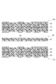
- FIG. 1 is a cross-sectional view showing an example of a cross-sectional configuration of a package substrate (multilayer substrate) according to an embodiment of the present invention.
- 2A and 2B are cross-sectional views showing a method for manufacturing the package substrate shown in FIG. 3A to 3C are cross-sectional views showing a method for manufacturing the package substrate shown in FIG. 1, illustrating a step performed after the step shown in FIG.
- FIG. 4 illustrates another example step that may be performed after the step illustrated in FIG.
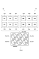
- FIG. 5 is a diagram for explaining a bonding process that reflects the results of the inspection process.
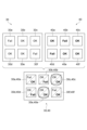
- FIG. 6 is a diagram for explaining a bonding process that reflects the results of the inspection process.
- FIG. 7 is a perspective view for explaining the bonding step of FIG. 5 and FIG.
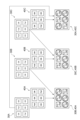
- FIG. 8 is a diagram for explaining a process of bonding a plurality of substrates together without reflecting the results of the inspection process.
- FIG. 9 is a diagram for explaining a process of performing a selection process reflecting the results of the inspection process and then bonding the substrates together when there are a plurality of substrates.
- the term “layer” includes structures that are formed over the entire surface when viewed in a plan view, as well as structures that are formed on only a portion of the surface.
- the term “process” includes not only independent processes, but also processes that cannot be clearly distinguished from other processes as long as the intended effect of the process is achieved.
- a numerical range indicated using “ ⁇ ” indicates a range that includes the numerical values before and after " ⁇ " as the minimum and maximum values, respectively.
- the upper or lower limit of a numerical range in one stage may be replaced with the upper or lower limit of a numerical range in another stage.
- the upper or lower limit of the numerical range may be replaced with a value shown in the examples.
- FIG. 1 is a diagram showing an example of a package substrate manufactured by a manufacturing method according to one embodiment of the present invention.
- the package substrate 1 (multilayer substrate, third laminate substrate) is a substrate having eight wiring layers.
- the package substrate 1 has a first wiring layer 11, a second wiring layer 12, a third wiring layer 13, a fourth wiring layer 14, a fifth wiring layer 15, a sixth wiring layer 16, a seventh wiring layer 17, an eighth wiring layer 18, a first insulating layer 21, a second insulating layer 22, a third insulating layer 23, a fourth insulating layer 24, a fifth insulating layer 25, a sixth insulating layer 26, and a seventh insulating layer 27.
- Each of the wiring layers from the first wiring layer 11 to the eighth wiring layer 18 can be formed, for example, by a subtractive method or a semi-additive method. Other methods may also be used.
- the first wiring layer 11 to the eighth wiring layer 18 are formed, for example, from a metal such as copper.
- the thickness of the first wiring layer 11 to the eighth wiring layer 18 is, for example, 5 ⁇ m to 35 ⁇ m, and preferably 9 ⁇ m to 25 ⁇ m.
- the first insulating layer 21 to the seventh insulating layer 27 are formed, for example, containing a hardening resin such as a thermosetting resin, and are hardened products of the hardening resin in the state of the package substrate 1.
- the first insulating layer 21 to the seventh insulating layer 27 may be configured to contain glass cloth G in the hardening resin, or may not contain glass cloth G.
- the first insulating layer 21 to the seventh insulating layer 27 are, for example, hardened products of prepreg.
- the first insulating layer 21 to the seventh insulating layer 27 may be formed from a glass substrate.
- Each of the first insulating layer 21 to the seventh insulating layer 27 is disposed between each of the first wiring layer 11 to the eighth wiring layer 18, thereby ensuring insulation between the wiring layers.
- the first insulating layer 21 to the seventh insulating layer 27 may be provided with vias (microvias) that penetrate each insulating layer, and such vias are configured to provide the necessary electrical continuity between the wiring layers.
- a package substrate 1 may be, for example, a package substrate for FC-BGA.
- the package substrate 1 shown in FIG. 1 has eight wiring layers (first wiring layer 11 to eighth wiring layer 18), it is not limited to this and may have six wiring layers, 12 wiring layers, 16 wiring layers, or 24 wiring layers.
- Figures 2(a) and 2(b) are cross-sectional views showing the method for manufacturing the package substrate shown in Figure 1.
- Figure 3 is a cross-sectional view showing the method for manufacturing the package substrate shown in Figure 1, showing a step carried out after the step shown in Figure 2. This manufacturing method includes the following steps [A] to [J].
- Step A A step of preparing a first substrate having a first insulating layer, a first wiring provided on a first surface of the first insulating layer, a second wiring provided on a second surface of the first insulating layer, and a first via that penetrates the first insulating layer and connects the first wiring and the second wiring to each other.
- Step B A step of preparing a second substrate having a second insulating layer, a third wiring provided on a first surface of the second insulating layer, a fourth wiring provided on a second surface of the second insulating layer, and a second via that penetrates the second insulating layer and connects the third wiring and the fourth wiring to each other.
- Step C A step of preparing a third substrate having a third insulating layer, a fifth wiring provided on a first surface of the third insulating layer, a sixth wiring provided on a second surface of the third insulating layer, and a third via penetrating the third insulating layer and connecting the fifth wiring and the sixth wiring to each other.
- Step D A step of preparing a fourth substrate having a fourth insulating layer, a seventh wiring provided on a first surface of the fourth insulating layer, an eighth wiring provided on a second surface of the fourth insulating layer, and a fourth via that penetrates the fourth insulating layer and connects the seventh wiring and the eighth wiring to each other.
- Step E A step of preparing a first bonding body having a first bonding material and a first connection via penetrating the first bonding material.
- Step F A step of preparing a third bonding body having a third bonding material and a third connection via penetrating the third bonding material.
- Step G A step of preparing a second bonding body having a second bonding material and a second connection via penetrating the second bonding material.
- Step H A step of stacking the first substrate and the second substrate with the first bonding body sandwiched therebetween to produce a first laminated substrate.
- Step I A step of producing a second laminated substrate by laminating a third substrate and a fourth substrate with a third bonded body sandwiched therebetween.
- Step J A step of stacking the first laminate substrate and the second laminate substrate so as to sandwich the second bonded body therebetween to produce a multilayer substrate.
- a first substrate 30 is prepared.
- the first substrate 30 has an insulating layer 31 (first insulating layer), a wiring layer 32 (first wiring) provided on a first surface 31a of the insulating layer 31, a wiring layer 33 (second wiring) provided on a second surface 31b of the insulating layer 31, and a via 34 (first via) that penetrates the insulating layer 31 and connects the wiring layer 32 and the wiring layer 33 to each other.
- the insulating layer 31 is composed of a thermosetting resin such as an epoxy resin, and is formed, for example, from a prepreg containing glass cloth G.
- the resin composition constituting the insulating layer 31 may contain a phenolic resin compound, an acid anhydride compound, an amine compound, or a hydrazide compound as a curing agent.
- the insulating layer 31 is a cured product (so-called C stage) formed by curing the prepreg or the like. In the cured state, the insulating layer 31 has a thickness of, for example, 7 ⁇ m to 100 ⁇ m, and preferably 20 ⁇ m to 60 ⁇ m.
- the insulating layer 31 may be a glass substrate.
- a wiring layer 32 is formed on the first surface 31a of the insulating layer 31.
- a wiring layer 33 is formed on the second surface 31b of the insulating layer 31.
- the wiring layers 32, 33 are wirings made of metal such as copper, gold, silver, etc., and can be formed in the insulating layer 31 by a subtractive method or a semi-additive method. They may also be formed by other methods.
- the wiring layers 32, 33 may be a metal plating layer, a metal foil such as copper foil, a layer formed by deposition such as sputtering, or a metal sintered layer.
- the thickness of the wiring layers 32, 33 may be, for example, 5 ⁇ m to 35 ⁇ m.
- the insulating layer 31 may further have a via 34 formed therein, which penetrates the insulating layer 31 in the stacking direction and connects the wiring layer 32 and the wiring layer 33 to each other.
- the via 34 is formed of a metal such as copper.
- the second substrate 40 is prepared.
- the second substrate 40 has the same configuration as the first substrate 30, and includes an insulating layer 41 (second insulating layer), a wiring layer 42 (third wiring) provided on the first surface 41a of the insulating layer 41, a wiring layer 43 (fourth wiring) provided on the second surface 41b of the insulating layer 41, and a via 44 (second via) that penetrates the insulating layer 41 and connects the wiring layer 42 and the wiring layer 43 to each other.
- the materials and forming methods of the insulating layer 41 and the wiring layers 42 and 43 of the second substrate 40 are the same as those of the first substrate 30, and therefore will not be described in detail.
- a third substrate 50 is prepared.
- the third substrate 50 has the same configuration as the first substrate 30, and includes an insulating layer 51 (third insulating layer), a wiring layer 52 (fifth wiring) provided on a first surface 51a of the insulating layer 51, a wiring layer 53 (sixth wiring) provided on a second surface 51b of the insulating layer 51, and a via 54 (third via) that penetrates the insulating layer 51 and connects the wiring layer 52 and the wiring layer 53 to each other.
- the materials and forming methods of the insulating layer 51 and the wiring layers 52 and 53 of the third substrate 50 are the same as those of the first substrate 30, and therefore will not be described in detail.
- a fourth substrate 60 is prepared.
- the fourth substrate 60 has the same configuration as the first substrate 30, and includes an insulating layer 61 (fourth insulating layer), a wiring layer 62 (seventh wiring) provided on a first surface 61a of the insulating layer 61, a wiring layer 63 (eighth wiring) provided on a second surface 61b of the insulating layer 61, and a via 64 (fourth via) that penetrates the insulating layer 61 and connects the wiring layer 62 and the wiring layer 63 to each other.
- the materials and forming methods of the insulating layer 61 and the wiring layers 62 and 63 of the fourth substrate 60 are the same as those of the first substrate 30, and therefore detailed description thereof will be omitted.
- a bonding body 70 (first bonding body) is prepared.
- the bonding body 70 has a bonding material 71 (first bonding material) and a connection via 72 (first connection via) penetrating the bonding material 71.
- the bonding material 71 of the bonding body 70 is a member that bonds the first substrate 10 and the second substrate 20, and is, for example, a semi-cured (B stage) or uncured state of a curable resin such as a thermosetting resin, and is composed of a prepreg containing a glass cloth G.
- the bonding material 71 is formed of a resin or the like and has insulating properties.
- the bonding material 71 is provided with a connection via 72 that penetrates the bonding material 71.
- connection via 72 is formed of a metal such as copper.
- the bonding material 71 is preferably composed of the same prepreg as the insulating layers 31, 41, 51, and 61, but the bonding material 71 is different in that it is in a semi-cured or uncured state before bonding (before step H described later) because it is a member for bonding.
- a bonded body 80 (third bonded body) is prepared.
- the bonded body 80 like the bonded body 70, has a bonding material 81 (third bonding material) and a connection via 82 (third connection via) penetrating the bonding material 81.
- the materials and the formation method of the bonding material 81 (insulating layer) and the connection via 82 of the bonded body 80 are similar to those of the bonded body 70, and therefore detailed description thereof will be omitted.
- a bonded body 90 (second bonded body) is prepared (see FIG. 3). Like the bonded body 70, the bonded body 90 has a bonding material 91 (second bonding material) and a connection via 92 (second connection via) penetrating the bonding material 91.
- the materials and the method of forming the bonding material 91 (insulating layer) and the connection via 92 of the bonded body 90 are the same as those of the bonded body 70, and therefore detailed description thereof will be omitted.
- step H As shown in (a) and (b) of FIG. 2, when the preparation of the first substrate 30, the second substrate 40, and the bonded body 70 is completed, the first substrate 30 and the second substrate 40 are laminated so that the bonded body 70 is sandwiched between the first substrate 30 and the second substrate 40 to produce the first laminated substrate 100. That is, the bonded body 70 in a semi-cured or uncured state is sandwiched between the first substrate 30 and the second substrate 40 to function as an adhesive, and the first substrate 30 and the second substrate 40 are bonded to form a laminate. Thereafter, the laminate is heated and pressurized to cure the bonded body 70 in a semi-cured or uncured state, and the first laminated substrate 100 is produced.
- the temperature for curing is, for example, 100° C. to 250° C., and the pressure when pressing is 0.2 to 10 MPa. Furthermore, since the insulating layers 31, 41 of the first substrate 30 and the second substrate 40 are a cured product of a curable resin or a glass substrate, even if they are heated in process H, the wiring layers 32, 33, the wiring layers 42, 43, and the vias 34, 44 will not shift from their original positions.
- step I when the preparation of the third substrate 50, the fourth substrate 60, and the bonded body 80 is completed, the third substrate 50 and the fourth substrate 60 are laminated so that the bonded body 80 is sandwiched between the third substrate 50 and the fourth substrate 60 to produce the second laminated substrate 110. That is, similar to the first laminated substrate 100, the bonded body 80 in a semi-cured or uncured state is sandwiched between the third substrate 50 and the fourth substrate 60 to function as an adhesive, and the third substrate 50 and the fourth substrate 60 are bonded to form a laminate. Thereafter, the laminate is heated and pressurized to cure the bonded body 80 in a semi-cured or uncured state, and the second laminated substrate 110 is produced.
- the temperature and pressure for curing are the same as those for producing the first laminated substrate 100. Furthermore, since the insulating layers 51, 61 of the third substrate 50 and the fourth substrate 60 are a cured product of a curable resin or a glass substrate, even if they are heated in step I, the wiring layers 52, 53, the wiring layers 62, 63, and the vias 54, 64 will not shift from their original positions.
- step J As shown in FIG. 3, when the preparation of the first laminated substrate 100, the second laminated substrate 110, and the bonded body 90 is completed, the first laminated substrate 100 and the second laminated substrate 110 are laminated so that the bonded body 90 is sandwiched between the first laminated substrate 100 and the second laminated substrate 110 to produce the package substrate 1. That is, the bonded body 90 in a semi-cured or uncured state is sandwiched between the first laminated substrate 100 and the second laminated substrate 110 to function as an adhesive, and the first laminated substrate 100 and the second laminated substrate 110 are bonded to form a laminate. Thereafter, the laminate is heated and pressurized to cure the bonded body 90 in a semi-cured or uncured state, and the package substrate 1 (see FIG.
- each insulating layer of the first laminate substrate 100 and the second laminate substrate 110 is a cured product of a curable resin or a glass substrate, even if reheated in process J, the wiring layers 32, 33, the wiring layers 42, 43, the wiring layers 52, 53, the wiring layers 62, 63, and the vias 34, 44, 54, 64 will not shift from their original positions.
- a laminate may be formed by sandwiching a semi-cured or uncured adhesive 90 between a first laminated substrate 100, which is a laminated substrate having four wiring layers, and a third substrate 50, which has two wiring layers, to function as an adhesive, and bonding the first laminated substrate 100 and a second laminated substrate 110A including the third substrate 50.
- the laminate may then be heated and pressurized to harden the semi-cured or uncured adhesive 90, thereby producing a six-layer package substrate.
- external terminals may be formed on the outermost layer of the package substrate 1, which is a multilayer substrate obtained after the first laminate substrate 100 and the second laminate substrate 110 are laminated and cured. This produces a package substrate having external terminals. It is also possible to manufacture a semiconductor device by mounting a semiconductor element on the package substrate thus produced.
- the first laminated substrate 100 is manufactured by stacking the first substrate 30 and the second substrate 40 so as to sandwich the joint 70 therebetween, and the third substrate 50 and the fourth substrate 60 are stacked so as to sandwich the joint 80 therebetween, or the second laminated substrate 110, 110A is manufactured so as to include the third substrate 50.
- the package substrate 1 is manufactured by stacking the first laminated substrate 100 and the second laminated substrate 110, 110A so as to sandwich the joint 90 therebetween.
- the time required to manufacture the package substrate 1 can be shortened compared to a method of stacking layers one by one.
- each laminate plate is not a stack of many substrates, misalignment in each wiring layer is unlikely to occur. Therefore, according to this method for manufacturing a package substrate, it is possible to efficiently manufacture a package substrate, which is a multilayer substrate, while suppressing misalignment in each wiring layer.
- the insulating layers 31, 41, 51, and 61 are insulating layers containing a hardened thermosetting resin.
- the insulating layers are not melted by heating in the subsequent lamination process, etc., and misalignment of the wiring layers is unlikely to occur. Therefore, according to this method for manufacturing a package substrate, misalignment of the wiring layers can be more reliably suppressed.
- the insulating layers 31, 41, 51, and 61 may be glass substrates.
- the insulating layers are not melted by heating in the subsequent lamination process, etc., and misalignment of the wiring layers is unlikely to occur. Therefore, this method for manufacturing a package substrate can more reliably suppress misalignment of the wiring layers.
- the bonding body 70 is preferably an insulating layer containing a semi-cured or uncured thermosetting resin before the first laminate substrate 100 is produced.
- the bonding body 80 is preferably an insulating layer containing a semi-cured or uncured thermosetting resin before the second laminate substrate 110 is produced. In this case, the bonding between the first substrate 30 and the second substrate 40 and the bonding between the third substrate 50 and the fourth substrate 60 can be performed reliably and easily.
- the bonding body 90 is preferably an insulating layer containing a semi-cured or uncured thermosetting resin before the package substrate 1 is produced. In this case, the bonding between the first laminate substrate 100 and the second laminate substrate 110 can be performed reliably and easily.
- connection vias 72 and 82 may be provided at positions in a planar direction different from the vias 34 and 54 and the vias 44 and 64. In this case, the degree of freedom in designing the wiring pattern in each wiring layer can be improved.
- two package substrates 1 formed by bonding and curing the first laminate substrate 100 and the second laminate substrate 110 with the bonding material 90 may be produced as the third laminate substrate, and another bonding material (fourth bonding material) having a similar configuration to the bonding material 90 may be sandwiched between the two package substrates 1 (third laminate substrates) and cured to produce a package substrate (fourth laminate substrate) having 16 wiring layers.
- this other bonding material has a bonding material (fourth bonding material) and connection vias (fourth connection vias) that penetrate the bonding material.
- each substrate is laminated and then bonded together as a unit.
- a continuity test may be performed on the wiring portions 30a-30f, 40a-40f included in each substrate, as shown in FIG. 5 and FIG. 6.
- each substrate is a large substrate including a plurality of wiring portions
- the continuity test is performed by testing the continuity and insulation of each wiring portion from both sides of the substrate using a flying probe or the like. If the result of the continuity test indicates that a wiring portion is defective (Fail) (see FIG. 6), the overall yield rate (yield) can be improved by not manufacturing that portion or not using that substrate.
- Figure 5 shows a case where all wiring parts are good (OK), while Figure 6 shows a case where some wiring parts are defective (Fail).
- wiring parts 30c, 40c and wiring parts 30e, 40e which are overlapping good (OK), are used as the subsequent product, and since it is clear that the other wiring parts are defective (Fail), subsequent inspections can be omitted.
- each wiring portion in each of the multiple first substrates 30A-30C may be inspected (determined as OK or Fail) and each wiring portion in each of the multiple second substrates 40A-40C may be inspected (determined as OK or Fail) as shown in Fig. 8.
- corresponding first substrates 30A and second substrates 40A, corresponding first substrates 30B and second substrates 40B, and corresponding first substrates 30C and second substrates 40C may be bonded together with respective bonding bodies 70 as shown in Fig. 8.
- the number of overlapping non-defective wiring portions is seven.
- a selection process may be performed so that more wiring sections determined to be good are overlapped, as shown in FIG. 9, and the first substrate and the second substrate may be bonded together.
- the number of overlapping good wiring sections is 11.
- This selection process may be performed by using a computer to calculate the quality rate (yield) when all substrates are combined, or other processing methods may be used.
Landscapes
- Engineering & Computer Science (AREA)
- Manufacturing & Machinery (AREA)
- Microelectronics & Electronic Packaging (AREA)
- Production Of Multi-Layered Print Wiring Board (AREA)
Abstract
Description
工程B:第2絶縁層と、第2絶縁層の第1面に設けられた第3配線と、第2絶縁層の第2面に設けられた第4配線と、第2絶縁層を貫通し第3配線及び第4配線を互いに接続する第2ビアとを有する第2基板を準備する工程。
工程C:第3絶縁層と、第3絶縁層の第1面に設けられた第5配線と、第3絶縁層の第2面に設けられた第6配線と、第3絶縁層を貫通し第5配線及び第6配線を互いに接続する第3ビアとを有する第3基板を準備する工程。
工程D:第4絶縁層と、第4絶縁層の第1面に設けられた第7配線と、第4絶縁層の第2面に設けられた第8配線と、第4絶縁層を貫通し第7配線及び第8配線を互いに接続する第4ビアとを有する第4基板を準備する工程。
工程E:第1接合材と、第1接合材を貫通する第1接続ビアとを有する第1接合体を準備する工程。
工程F:第3接合材と、第3接合材を貫通する第3接続ビアとを有する第3接合体を準備する工程。
工程G:第2接合材と、第2接合材を貫通する第2接続ビアとを有する第2接合体を準備する工程。
工程H:第1接合体をその間に挟み込むように第1基板と第2基板とを積層して第1積層基板を作製する工程。
工程I:第3接合体をその間に挟み込むように第3基板と第4基板とを積層して第2積層基板を作製する工程。
工程J:第2接合体をその間に挟み込むように第1積層基板と第2積層基板とを積層して多層基板を作製する工程。
工程Aでは、図2の(a)に示すように、第1基板30を準備する。第1基板30は、絶縁層31(第1絶縁層)と、絶縁層31の第1面31aに設けられた配線層32(第1配線)と、絶縁層31の第2面31bに設けられた配線層33(第2配線)と、絶縁層31を貫通し、配線層32及び配線層33を互いに接続するビア34(第1ビア)と、を有している。
工程Bでは、第2基板40を準備する。第2基板40は、第1基板30と同様の構成を有しており、絶縁層41(第2絶縁層)と、絶縁層41の第1面41aに設けられた配線層42(第3配線)と、絶縁層41の第2面41bに設けられた配線層43(第4配線)と、絶縁層41を貫通し、配線層42及び配線層43を互いに接続するビア44(第2ビア)と、を有している。第2基板40の絶縁層41及び配線層42,43の材料及び形成方法は、第1基板30と同様であるため、詳細な説明は省略する。
工程Cでは、第3基板50を準備する。第3基板50は、第1基板30と同様の構成を有しており、絶縁層51(第3絶縁層)と、絶縁層51の第1面51aに設けられた配線層52(第5配線)と、絶縁層51の第2面51bに設けられた配線層53(第6配線)と、絶縁層51を貫通し、配線層52及び配線層53を互いに接続するビア54(第3ビア)と、を有している。第3基板50の絶縁層51及び配線層52,53の材料及び形成方法は、第1基板30と同様であるため、詳細な説明は省略する。
工程Dでは、第4基板60を準備する。第4基板60は、第1基板30と同様の構成を有しており、絶縁層61(第4絶縁層)と、絶縁層61の第1面61aに設けられた配線層62(第7配線)と、絶縁層61の第2面61bに設けられた配線層63(第8配線)と、絶縁層61を貫通し、配線層62及び配線層63を互いに接続するビア64(第4ビア)と、を有している。第4基板60の絶縁層61及び配線層62,63の材料及び形成方法は、第1基板30と同様であるため、詳細な説明は省略する。
工程Eでは、接合体70(第1接合体)を準備する。接合体70は、接合材71(第1接合材)と、接合材71を貫通する接続ビア72(第1接続ビア)とを有する。接合体70の接合材71は、第1基板10と第2基板20とを接合する部材であり、例えば、熱硬化性樹脂等の硬化性樹脂の半硬化(Bステージ)又は未硬化の状態のものであり、ガラスクロスGを含むプリプレグなどから構成されている。接合材71は、樹脂等から形成されており、絶縁性を有している。この接合材71には、接合材71を貫通する接続ビア72が設けられている。接続ビア72は、例えば、銅等の金属から形成されている。接合材71は、絶縁層31,41,51,61と同じプリプレグから構成されていることが好ましいが、接合材71は、接合するための部材であることから、接合を行う前(後述する工程Hの前)においては、半硬化又は未硬化の状態となっている点が相違する。
工程Fでは、接合体80(第3接合体)を準備する。接合体80は、接合体70と同様に、接合材81(第3接合材)と、接合材81を貫通する接続ビア82(第3接続ビア)とを有している。接合体80の接合材81(絶縁層)及び接続ビア82の材料及び形成方法は、接合体70と同様であるため、詳細な説明は省略する。
工程Gでは、接合体90(第2接合体)を準備する(図3を参照)。接合体90は、接合体70と同様に、接合材91(第2接合材)と、接合材91を貫通する接続ビア92(第2接続ビア)とを有している。接合体90の接合材91(絶縁層)及び接続ビア92の材料及び形成方法は、接合体70と同様であるため、詳細な説明は省略する。
工程Hでは、図2の(a)及び(b)に示すように、第1基板30、第2基板40及び接合体70の準備が終了すると、接合体70を第1基板30と第2基板40との間に挟み込むように第1基板30と第2基板40とを積層して第1積層基板100を作製する。即ち、第1基板30と第2基板40との間に、半硬化又は未硬化状態の接合体70を挟み込んで接着剤として機能させて、第1基板30と第2基板40とを接合して積層体を形成する。その後、積層体に対して、加熱及び加圧を行い、半硬化又は未硬化状態の接合体70を硬化させ、第1積層基板100を作製する。硬化するための温度は、例えば100℃~250℃であり、加圧する際の圧力は0.2~10MPaである。なお、第1基板30及び第2基板40の絶縁層31,41は、硬化性樹脂の硬化物又はガラス基板であることから、工程Hにおいて加熱しても、配線層32,33、配線層42,43、ビア34,44が当初の位置からずれてしまうことはない。
工程Iでは、第3基板50、第4基板60及び接合体80の準備が終了すると、接合体80を第3基板50と第4基板60との間に挟み込むように第3基板50と第4基板60とを積層して第2積層基板110を作製する。即ち、第1積層基板100と同様に、第3基板50と第4基板60との間に、半硬化又は未硬化状態の接合体80を挟み込んで接着剤として機能させて、第3基板50と第4基板60とを接合して積層体を形成する。その後、積層体に対して、加熱及び加圧を行い、半硬化又は未硬化状態の接合体80を硬化させ、第2積層基板110を作製する。硬化するための温度及び圧力は、第1積層基板100を作製する場合と同様である。なお、第3基板50及び第4基板60の絶縁層51,61は、硬化性樹脂の硬化物又はガラス基板であることから、工程Iにおいて加熱しても、配線層52,53、配線層62,63、ビア54,64が当初の位置からずれてしまうことはない。
工程Jでは、図3に示すように、第1積層基板100、第2積層基板110、及び、接合体90の準備が終了すると、接合体90を第1積層基板100と第2積層基板110との間に挟み込むように第1積層基板100と第2積層基板110とを積層してパッケージ基板1を作製する。即ち、第1積層基板100と第2積層基板110との間に、半硬化又は未硬化状態の接合体90を挟み込んで接着剤として機能させて、第1積層基板100と第2積層基板110とを接合して積層体を形成する。その後、積層体に対して、加熱及び加圧を行い、半硬化又は未硬化状態の接合体90を硬化させ、パッケージ基板1(図1参照)を作製する。硬化するための温度及び圧力は、第1積層基板100等を作製する場合と同様である。なお、第1積層基板100及び第2積層基板110の各絶縁層は、硬化性樹脂の硬化物又はガラス基板であることから、工程Jにおいて再加熱しても、配線層32,33、配線層42,43、配線層52,53、配線層62,63、ビア34,44,54,64が当初の位置からずれてしまうことはない。
Claims (14)
- 第1絶縁層と、前記第1絶縁層の第1面に設けられた第1配線と、前記第1絶縁層の第2面に設けられた第2配線と、前記第1絶縁層を貫通し前記第1配線及び前記第2配線を互いに接続する第1ビアとを有する第1基板を準備する工程と、
第2絶縁層と、前記第2絶縁層の第1面に設けられた第3配線と、前記第2絶縁層の第2面に設けられた第4配線と、前記第2絶縁層を貫通し前記第3配線及び前記第4配線を互いに接続する第2ビアとを有する第2基板を準備する工程と、
第3絶縁層と、前記第3絶縁層の第1面に設けられた第5配線と、前記第3絶縁層の第2面に設けられた第6配線と、前記第3絶縁層を貫通し前記第5配線及び前記第6配線を互いに接続する第3ビアとを有する第3基板を準備する工程と、
第1接合材と、前記第1接合材を貫通する第1接続ビアとを有する第1接合体を準備する工程と、
第2接合材と、前記第2接合材を貫通する第2接続ビアとを有する第2接合体を準備する工程と、
前記第1接合体をその間に挟み込むように前記第1基板と前記第2基板とを積層して第1積層基板を作製する工程と、
前記第3基板を含む第2積層基板を準備する工程と、
前記第2接合体をその間に挟み込むように前記第1積層基板と前記第2積層基板とを積層して第3積層基板を作製する工程と、
を備える多層基板の製造方法。 - 第4絶縁層と、前記第4絶縁層の第1面に設けられた第7配線と、前記第4絶縁層の第2面に設けられた第8配線と、前記第4絶縁層を貫通し前記第7配線及び前記第8配線を互いに接続する第4ビアとを有する第4基板を準備する工程と、
第3接合材と、前記第3接合材を貫通する第3接続ビアとを有する第3接合体を準備する工程と、を備え、
前記第2積層基板を準備する工程では、前記第3接合体をその間に挟み込むように前記第3基板と前記第4基板とを積層して前記第2積層基板を作製する、
請求項1に記載の多層基板の製造方法。 - 前記第1絶縁層、前記第2絶縁層、前記第3絶縁層、及び前記第4絶縁層は、硬化された硬化性樹脂を含む絶縁層である、
請求項1又は2に記載の多層基板の製造方法。 - 前記第1絶縁層、前記第2絶縁層、前記第3絶縁層、及び前記第4絶縁層は、ガラス基板である、
請求項1又は2に記載の多層基板の製造方法。 - 前記第1接合材は、前記第1積層基板を作製する前において、半硬化又は未硬化の硬化性樹脂を含む絶縁層であり、
前記第2接合材は、前記第3積層基板を作製する前において、半硬化又は未硬化の硬化性樹脂を含む絶縁層である、
請求項1~4の何れか一項に記載の多層基板の製造方法。 - 前記第1ビア、前記第2ビア及び前記第1接続ビアのうち少なくとも1つのビアは、他のビアとは異なる平面方向における位置に設けられている、
請求項1~5の何れか一項に記載の多層基板の製造方法。 - 前記第1接続ビアは、前記第1ビア及び前記第2ビアとは異なる平面方向における位置に設けられている、
請求項1~6の何れか一項に記載の多層基板の製造方法。 - 第4接合材と、前記第4接合材を貫通する第4接続ビアとを有する第4接合体を準備する工程を更に備え、
前記第3積層基板を作製する工程では、前記第2接合材をその間に挟み込むように前記第1積層基板と前記第2積層基板とを積層した第3積層基板を2つ作製し、
前記第4接合材をその間に挟み込むように2つの前記第3積層基板を積層して第4積層基板を作製する、
請求項1~7の何れか一項に記載の多層基板の製造方法。 - 前記多層基板の最外層に外部端子を形成する工程を更に備える、
請求項1~8の何れか一項に記載の多層基板の製造方法。 - 前記多層基板がパッケージ基板である、
請求項1~9の何れか一項に記載の多層基板の製造方法。 - 前記第1基板、前記第2基板、前記第3基板、及び第4基板のうち少なくとも1つの基板を、積層する前に、検査する工程を更に備える、
請求項1~10の何れか一項に記載の多層基板の製造方法。 - 前記第1基板を準備する工程では、複数の第1基板が準備され、
前記第2基板を準備する工程では、複数の第2基板が準備され、
前記第1積層基板を作製する工程では、複数の第1積層基板が作製され、
前記複数の第1基板のそれぞれ及び前記複数の第2基板のそれぞれは、複数の配線部を含む大判基板であり、
前記検査する工程では、前記複数の第1基板のそれぞれにおける各配線部が検査されると共に、前記複数の第2基板のそれぞれにおける各配線部が検査され、
前記第1積層基板を作製する工程では、前記検査する工程での検査結果に基づいて前記複数の第1基板の各基板と前記複数の第2基板の各基板との組み合わせが選択される、
請求項11に記載の多層基板の製造方法。 - 前記第1積層基板を作製する工程では、前記検査する工程で良品と判断された各配線部同士が重ね合わされるように選択が行われる、
請求項12に記載の多層基板の製造方法。 - 請求項1~13の何れか一項に記載の多層基板の製造方法によって製造されるパッケージ基板と、
前記パッケージ基板に実装される半導体素子と、
を備える半導体装置。
Priority Applications (3)
| Application Number | Priority Date | Filing Date | Title |
|---|---|---|---|
| JP2025525526A JPWO2024252560A1 (ja) | 2023-06-07 | 2023-06-07 | |
| PCT/JP2023/021163 WO2024252560A1 (ja) | 2023-06-07 | 2023-06-07 | 多層基板の製造方法、及び、半導体装置 |
| CN202380097530.XA CN121014264A (zh) | 2023-06-07 | 2023-06-07 | 多层基板的制造方法及半导体装置 |
Applications Claiming Priority (1)
| Application Number | Priority Date | Filing Date | Title |
|---|---|---|---|
| PCT/JP2023/021163 WO2024252560A1 (ja) | 2023-06-07 | 2023-06-07 | 多層基板の製造方法、及び、半導体装置 |
Publications (1)
| Publication Number | Publication Date |
|---|---|
| WO2024252560A1 true WO2024252560A1 (ja) | 2024-12-12 |
Family
ID=93795414
Family Applications (1)
| Application Number | Title | Priority Date | Filing Date |
|---|---|---|---|
| PCT/JP2023/021163 Ceased WO2024252560A1 (ja) | 2023-06-07 | 2023-06-07 | 多層基板の製造方法、及び、半導体装置 |
Country Status (3)
| Country | Link |
|---|---|
| JP (1) | JPWO2024252560A1 (ja) |
| CN (1) | CN121014264A (ja) |
| WO (1) | WO2024252560A1 (ja) |
Citations (5)
| Publication number | Priority date | Publication date | Assignee | Title |
|---|---|---|---|---|
| JP2000200976A (ja) * | 1999-01-05 | 2000-07-18 | Mitsubishi Plastics Ind Ltd | 多層プリント配線板およびその製造方法 |
| JP2007021801A (ja) * | 2005-07-13 | 2007-02-01 | Dainippon Printing Co Ltd | 積層装置および積層方法 |
| WO2007046459A1 (ja) * | 2005-10-20 | 2007-04-26 | Matsushita Electric Industrial Co., Ltd. | 多層プリント配線基板及びその製造方法 |
| JP2013077697A (ja) * | 2011-09-30 | 2013-04-25 | Murata Mfg Co Ltd | セラミック多層基板及びその製造方法 |
| JP2019036607A (ja) * | 2017-08-10 | 2019-03-07 | リード・エレクトロニクス株式会社 | 回路付きガラス基板含有多層配線板及びその製造方法 |
-
2023
- 2023-06-07 CN CN202380097530.XA patent/CN121014264A/zh active Pending
- 2023-06-07 WO PCT/JP2023/021163 patent/WO2024252560A1/ja not_active Ceased
- 2023-06-07 JP JP2025525526A patent/JPWO2024252560A1/ja active Pending
Patent Citations (5)
| Publication number | Priority date | Publication date | Assignee | Title |
|---|---|---|---|---|
| JP2000200976A (ja) * | 1999-01-05 | 2000-07-18 | Mitsubishi Plastics Ind Ltd | 多層プリント配線板およびその製造方法 |
| JP2007021801A (ja) * | 2005-07-13 | 2007-02-01 | Dainippon Printing Co Ltd | 積層装置および積層方法 |
| WO2007046459A1 (ja) * | 2005-10-20 | 2007-04-26 | Matsushita Electric Industrial Co., Ltd. | 多層プリント配線基板及びその製造方法 |
| JP2013077697A (ja) * | 2011-09-30 | 2013-04-25 | Murata Mfg Co Ltd | セラミック多層基板及びその製造方法 |
| JP2019036607A (ja) * | 2017-08-10 | 2019-03-07 | リード・エレクトロニクス株式会社 | 回路付きガラス基板含有多層配線板及びその製造方法 |
Also Published As
| Publication number | Publication date |
|---|---|
| JPWO2024252560A1 (ja) | 2024-12-12 |
| CN121014264A (zh) | 2025-11-25 |
Similar Documents
| Publication | Publication Date | Title |
|---|---|---|
| US5628852A (en) | Method for manufacturing a polyimide multilayer wiring substrate | |
| US5232548A (en) | Discrete fabrication of multi-layer thin film, wiring structures | |
| US5224265A (en) | Fabrication of discrete thin film wiring structures | |
| CN101325846B (zh) | 多层配线基板及其制造方法 | |
| CN101069459B (zh) | 多层印刷线路基板及其制造方法 | |
| US7956293B2 (en) | Multilayer printed wiring board and manufacturing method thereof | |
| JP2011023751A (ja) | 電子部品内蔵型多層印刷配線基板及びその製造方法 | |
| JPH04233266A (ja) | 多重積層型高密度相互接続構造とそれを製作する方法 | |
| US9736948B2 (en) | Systems and methods of manufacturing printed circuit boards using blind and internal micro vias to couple subassemblies | |
| JPH0828580B2 (ja) | 配線基板構造及びその製造方法 | |
| CN101241861A (zh) | 新型多层无芯支撑结构及其制作方法 | |
| US8453322B2 (en) | Manufacturing methods of multilayer printed circuit board having stacked via | |
| CN101112140A (zh) | 多层印刷线路基板及其制造方法 | |
| CN116456570A (zh) | 具有不对称堆叠件的部件承载件及其确定方法和制造方法 | |
| WO2025224934A1 (ja) | 多層基板の製造方法 | |
| US12108544B2 (en) | Multi-layer printed circuit board made of different materials and manufacturing method thereof | |
| CN121014264A (zh) | 多层基板的制造方法及半导体装置 | |
| JP2005123332A (ja) | 回路基板及びその製造方法 | |
| TWI461135B (zh) | 製作電路板之方法 | |
| TWI236324B (en) | Insulating structure of circuit board and method for fabricating the circuit board by using the insulating structure | |
| TWI886783B (zh) | 單側疊板方法 | |
| KR100704927B1 (ko) | 페이스트 범프를 이용한 인쇄회로기판 및 그 제조방법 | |
| CN113784496B (zh) | 具有树脂限流特性的印刷电路板及其制造方法 | |
| JP4186236B2 (ja) | ポリイミド多層配線フィルムの製造方法及び多層配線基板の製造方法 | |
| JP5126119B2 (ja) | 電子装置の製造方法 |
Legal Events
| Date | Code | Title | Description |
|---|---|---|---|
| 121 | Ep: the epo has been informed by wipo that ep was designated in this application |
Ref document number: 23940663 Country of ref document: EP Kind code of ref document: A1 |
|
| ENP | Entry into the national phase |
Ref document number: 2025525526 Country of ref document: JP Kind code of ref document: A |
|
| WWE | Wipo information: entry into national phase |
Ref document number: 2025525526 Country of ref document: JP |
|
| NENP | Non-entry into the national phase |
Ref country code: DE |
|
| 122 | Ep: pct application non-entry in european phase |
Ref document number: 23940663 Country of ref document: EP Kind code of ref document: A1 |