WO2024252675A1 - 半導体装置の製造方法、および表示装置の製造方法 - Google Patents
半導体装置の製造方法、および表示装置の製造方法 Download PDFInfo
- Publication number
- WO2024252675A1 WO2024252675A1 PCT/JP2023/021567 JP2023021567W WO2024252675A1 WO 2024252675 A1 WO2024252675 A1 WO 2024252675A1 JP 2023021567 W JP2023021567 W JP 2023021567W WO 2024252675 A1 WO2024252675 A1 WO 2024252675A1
- Authority
- WO
- WIPO (PCT)
- Prior art keywords
- semiconductor device
- conductive film
- manufacturing
- insulating substrate
- forming
- Prior art date
- Legal status (The legal status is an assumption and is not a legal conclusion. Google has not performed a legal analysis and makes no representation as to the accuracy of the status listed.)
- Ceased
Links
Images





Classifications
-
- H—ELECTRICITY
- H10—SEMICONDUCTOR DEVICES; ELECTRIC SOLID-STATE DEVICES NOT OTHERWISE PROVIDED FOR
- H10D—INORGANIC ELECTRIC SEMICONDUCTOR DEVICES
- H10D30/00—Field-effect transistors [FET]
- H10D30/01—Manufacture or treatment
- H10D30/021—Manufacture or treatment of FETs having insulated gates [IGFET]
-
- H—ELECTRICITY
- H10—SEMICONDUCTOR DEVICES; ELECTRIC SOLID-STATE DEVICES NOT OTHERWISE PROVIDED FOR
- H10D—INORGANIC ELECTRIC SEMICONDUCTOR DEVICES
- H10D30/00—Field-effect transistors [FET]
- H10D30/60—Insulated-gate field-effect transistors [IGFET]
- H10D30/67—Thin-film transistors [TFT]
-
- H—ELECTRICITY
- H10—SEMICONDUCTOR DEVICES; ELECTRIC SOLID-STATE DEVICES NOT OTHERWISE PROVIDED FOR
- H10P—GENERIC PROCESSES OR APPARATUS FOR THE MANUFACTURE OR TREATMENT OF DEVICES COVERED BY CLASS H10
- H10P14/00—Formation of materials, e.g. in the shape of layers or pillars
- H10P14/40—Formation of materials, e.g. in the shape of layers or pillars of conductive or resistive materials
-
- H—ELECTRICITY
- H10—SEMICONDUCTOR DEVICES; ELECTRIC SOLID-STATE DEVICES NOT OTHERWISE PROVIDED FOR
- H10W—GENERIC PACKAGES, INTERCONNECTIONS, CONNECTORS OR OTHER CONSTRUCTIONAL DETAILS OF DEVICES COVERED BY CLASS H10
- H10W20/00—Interconnections in chips, wafers or substrates
- H10W20/40—Interconnections external to wafers or substrates, e.g. back-end-of-line [BEOL] metallisations or vias connecting to gate electrodes
- H10W20/45—Interconnections external to wafers or substrates, e.g. back-end-of-line [BEOL] metallisations or vias connecting to gate electrodes characterised by their insulating parts
- H10W20/48—Insulating materials thereof
Definitions
- Patent Document 1 discloses that when fabricating a semiconductor device on a glass substrate, a thin film having electrical conductivity (e.g., a silicon film that has been made electrically conductive) is formed on the underside of the glass substrate in the early stages of the fabrication process.
- a thin film having electrical conductivity e.g., a silicon film that has been made electrically conductive
- electrostatic breakdown can cause defects and reduce the manufacturing yield of the semiconductor devices.
- the method for manufacturing a semiconductor device includes the steps of forming a conductive film on the upper surface of an insulating substrate, forming a base containing a resin on the upper surface of the conductive film, and forming a semiconductor device on an upper layer of the base.
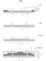
- FIG. 1A to 1C are cross-sectional views illustrating an example of a method for manufacturing a semiconductor device according to an embodiment of the present disclosure.
- 2 is a cross-sectional view illustrating an example of voltage loading according to the method shown in FIG. 1 .
- FIG. 11 is a cross-sectional view illustrating an example of voltage loading by a method in which a conductive film is not formed on an insulating substrate of a comparative example.
- 2 is a plan view perspective view showing an example of the positional relationship between the insulating substrate shown in FIG. 1, a patterned conductive film, and a resin contained in the base.
- FIG. 2 is a cross-sectional view showing a continuation of the example of the manufacturing method of the semiconductor device shown in FIG. 1 .
- FIG. 13 illustrates a transmittance graph according to an embodiment of the present disclosure.
- FIG. 5 is a cross-sectional view showing an example of reusing the insulating substrate shown in FIGS. 1 and 4.
- FIG. 5 is a cross-sectional view showing another example of reuse of the insulating substrate shown in FIGS. 1 and 4.
- 11A to 11C are cross-sectional views showing a modified example of the method for manufacturing a semiconductor device according to an embodiment of the present disclosure.
- 1A to 1C are cross-sectional views illustrating an example of a method for manufacturing a semiconductor device according to an embodiment of the present disclosure.
- 1A to 1C are cross-sectional views illustrating an example of a manufacturing method for a display device according to an embodiment of the present disclosure.
- FIG. 1 is a cross-sectional view showing an example of a method for manufacturing a semiconductor device according to an embodiment of the present disclosure.
- the method for manufacturing a semiconductor device includes a step of forming a conductive film 2 on an upper surface 1T of an insulating substrate 1 (step S10), a step of forming a base 3 containing a resin on an upper surface 2T of the conductive film 2 (step S30), and a step of forming a backplane 4 including a semiconductor device Tr on an upper layer above the base 3 (step S50).
- the insulating substrate 1 is, for example, a glass substrate.
- the semiconductor device Tr is, for example, a thin film transistor.
- forming element Y on the upper surface of element X means forming element Y after element X so that element Y is in direct contact with the upper surface of element X.
- Forming element Y in a layer above element X means forming element Y after element X, and includes both cases where element Y is in contact with the upper surface of element X and where it is not in contact with the upper surface of element X.
- a conductive film 2 is formed on the upper surface 1T of an insulating substrate 1.
- static electricity is generated by friction, and localized charges are generated on the insulating substrate 1.
- the conductive film 2 disperses the localized charges, reducing the amount of charge per area. This reduces the voltage load per area on the components formed above the conductive film 2, including the semiconductor device Tr.
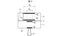
- FIG. 2 is a cross-sectional view for explaining an example of voltage loading by the method shown in FIG. 1.
- the layer between the conductive film 2 and the backplane 4 is ignored.
- the insulating substrate 1 is supported or carried by a support fixture ST such as a pin or an arm. Static electricity may be generated by contact or friction between the lower surface 1B of the insulating substrate 1 and the support fixture ST, and a charge -Q may be generated on the lower surface 1B.
- the charge -Q on the lower surface 1B of the insulating substrate 1 induces a charge +Q on the upper surface 1T
- the charge +Q on the upper surface 1T of the insulating substrate 1 induces a charge -Q on the lower surface of the backplane 4 via the conductive film 2.
- the charge -Q on the lower surface of the backplane 4 induces a charge +Q on the upper surface, and a voltage V 2 is applied between the upper and lower surfaces of the backplane 4.
- the area S 2 on the lower surface of the backplane 4 where the charges ⁇ Q are distributed is larger than the area S 1 on the upper surface 1T of the insulating substrate 1 where the charges +Q are distributed (S 1 ⁇ S 2 ).
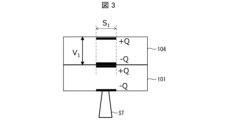
- FIG. 3 is a cross-sectional view for explaining an example of voltage loading by a method of forming no conductive film on an insulating substrate of a comparative example.
- the layer between the insulating substrate 101 and the backplane 104 is ignored.
- the charge -Q on the lower surface of the insulating substrate 1 induces a charge +Q on the upper surface
- the charge +Q on the upper surface of the insulating substrate 101 induces a charge -Q on the lower surface of the backplane 104.
- the charge -Q on the lower surface of the backplane 104 induces a charge +Q on the upper surface, and a voltage V 1 is applied between the upper and lower surfaces of the backplane 104. Since there is no conductive film, the area S 1 where the charge +Q is distributed on the upper surface of the insulating substrate 101 is equal to the area where the charge -Q is distributed on the lower surface of the backplane 104.
- the backplane 4, 104 can be considered as a parallel plate capacitor.
- a parallel plate capacitor it is known that the following relationship (1) holds true.
- Q ⁇ V ⁇ S/d...(1)
- Q Absolute value of the charge stored in the capacitor electrode
- ⁇ dielectric constant between the electrodes of the capacitor
- V absolute value of the voltage between the electrodes of the capacitor
- S electrode area of the capacitor
- d the distance between the electrodes of the capacitor.
- the inter-electrode voltages V1 and V2 and the electrode areas S1 and S2 are applied to the above relational expression (1) to obtain the relational expression (2). Furthermore, the electrode area S1 ⁇ S2 is applied to obtain the relational expression (3). Note that V1 , S1 , V2 , and S2 are greater than 0.
- the method according to the present disclosure can reduce the voltage load per area on the semiconductor device Tr.
- the manufacturing yield of the device Tr can be improved.
- a conductive film 2 is formed on the upper surface 1T of the insulating substrate 1, and a base 3 and a backplane 4 are formed above the conductive film 2. Therefore, the support tool ST supporting the insulating substrate 1 does not come into contact with the conductive film 2.
- the tool supporting the insulating substrate may come into contact with the conductive film, causing part of the conductive film to peel off. The peeled off pieces become foreign matter and reduce the manufacturing yield of the semiconductor device.
- a large amount of charge may move between the tool in contact and the conductive film, which may lead to electrostatic damage to the components.
- the method disclosed herein can improve the manufacturing yield of semiconductor devices including the backplane 4.
- the conductive film 2 is formed over the entire upper surface 1T of the insulating substrate 1.
- the method for manufacturing a semiconductor device according to the present disclosure further includes a step (step S20) of patterning the conductive film 2 so as to remove the outer edge portion 2S of the conductive film 2.
- the base 3 is formed so as to cover the upper surface 2T and side surface 2L of the patterned conductive film 2.
- the conductive film 2 is protected by the base 3, and peeling of the conductive film 2 can be reduced.
- the outer edge portion 2S of the conductive film 2 is the portion formed on the outer edge portion of the upper surface 1T of the insulating substrate 1.
- a first resin layer R1 is formed on the upper surface 2T of the conductive film 2, an intermediate layer ML is formed above the first resin layer R1, and a second resin layer R2 is formed above the intermediate layer ML.
- the first resin layer R1 and the second resin layer R2 may contain a resin such as polyimide.
- the intermediate layer ML may contain an inorganic material such as silicon nitride, silicon oxide, and silicon oxynitride.
- FIG. 4 is a plan view perspective view showing an example of the positional relationship between the insulating substrate shown in FIG. 1, the patterned conductive film, and the resin contained in the base.
- the outer periphery of the resin contained in the base 3 is located between the outer periphery of the insulating substrate 1 and the outer periphery of the conductive film 2.
- the distance between the outer periphery of the insulating substrate 1 and the outer periphery of the conductive film 2 may be 18 to 19 mm.
- the first resin layer R1 contained in the base 3 is in direct contact with the insulating substrate 1 at its outer edge.
- the method for manufacturing a semiconductor device according to the present disclosure further includes a step (step S40) of forming a base coat BC above the undercoat 3, and forming a semiconductor device Tr above the base coat BC.
- a step S40 of forming a base coat BC above the undercoat 3, and forming a semiconductor device Tr above the base coat BC.
- the conductive film 2 may include a transparent metal oxide, for example, one or more selected from the group including indium tin oxide (ITO), indium zinc oxide (IZO), and indium gallium zinc oxide (InGaZnO).
- the conductive film 2 may include a conductive organic material, for example, one or more selected from the group including carbon nanotubes, graphene, and fullerene.
- the conductive film 2 may be a semiconductor thin film, such as a silicon thin film, doped with impurity ions that impart conductivity.
- the impurities that impart conductivity to the silicon thin film include phosphorus ions or boron ions.
- the conductive film 2 is made of a material that can withstand heat generated in processes subsequent to step S10, such as the process of forming the semiconductor device Tr.
- the conductive film 2 may have heat resistance of 400°C to 500°C.
- the conductive film 2 may be in an electrically floating state.
- An opening may be provided in the base 3, and the conductive film 2 may be electrically connected to the wiring layer in the backplane 4 through this opening. This electrical connection is separated by a process (step S70) of peeling the base 3 from the insulating substrate 1, which will be described later.
- step S10 the conductive film 2 is formed over the entire upper surface 1T of the insulating substrate 1. Also, the conductive film 2 is formed only on the upper surface 1T of the insulating substrate 1. Because the lower surface 1B and side surface 1L of the insulating substrate 1 remain non-conductive, even if the support fixture ST comes into contact with the lower surface 1B or side surface 1L, it is difficult for charges to transfer between the support fixture ST and the insulating substrate 1. Therefore, electrostatic breakdown caused by charge transfer with the support fixture ST can be reduced.
- FIG. 5 is a cross-sectional view showing a continuation of the example of the method for manufacturing the semiconductor device shown in FIG. 1.
- the method for manufacturing the semiconductor device further includes a step of irradiating the base 3 with a laser from below the insulating substrate 1 (step S60) and a step of peeling the base 3 from the insulating substrate 1 (step S70).
- the resin of the base 3 is denatured by the laser irradiation, making it easier to peel off. For this reason, it is beneficial for the insulating substrate 1 and the conductive film 2 to have a high laser transmittance.
- the conductive film 2 may have a laser transmittance of 60% or more.
- the insulating substrate 1 and the conductive film 2 may have a laser transmittance of 60% or more in total.
- the central wavelength of the laser irradiated in step S60 is, for example, 343 [nm].
- the conductive film 2 mostly remains on the insulating substrate 1.
- FIG. 6 is a diagram showing a transmittance graph according to an embodiment of the present disclosure.
- the dashed line shows a transmittance graph of only the glass substrate as a reference example.
- “with annealing” shows a transmittance graph of the glass substrate and the ITO thin film in a case where an ITO thin film having an average thickness of 42 nm is formed on the glass substrate and the ITO thin film is annealed at 500°C.
- “without annealing” shows a transmittance graph of the glass substrate and the ITO thin film in a case where an ITO thin film having an average thickness of 24 to 42 nm is formed on the glass substrate and the ITO thin film is not annealed.
- the vertical axis of FIG. 6 shows transmittance [%], and the horizontal axis shows wavelength [nm].
- the transmittance of the glass substrate alone is less than 90%, and the total transmittance of the glass substrate and the ITO thin film is approximately 54% or more.
- the laser transmittance of any of the ITO thin films in the examples shown in the transmittance graphs by solid lines in FIG. 6 is approximately 60% or more.
- the manufacturing method of the semiconductor device according to the present disclosure to further include a step of annealing the conductive film 2.
- FIG. 7 is a cross-sectional view showing an example of reusing the insulating substrate shown in FIGS. 1 and 4.
- the insulating substrate 1 and the conductive film 2 may be reused after the base 3 has been peeled off.
- unnecessary films such as the intermediate layer ML and the base coat BC remain on the insulating substrate 1 in step S70, the unnecessary films are removed from the insulating substrate 1 (step S80), and then the processes from step S30 onwards are carried out again.
- FIG. 8 is a cross-sectional view showing another example of the reuse of the insulating substrate shown in FIG. 1 and FIG. 4.
- the insulating substrate 1 may be reused by removing the upper film UF above the insulating substrate 1 from the insulating substrate 1 after peeling off the base 3.
- the upper film UF may include the conductive film 2.
- the upper film UF including the conductive film 2, the intermediate layer ML, and the base coat BC is removed from the insulating substrate 1 (step S90), and then the processes from step S10 onwards are performed again.
- (Modification) 9 is a cross-sectional view showing a modified example of the method for manufacturing a semiconductor device according to an embodiment of the present disclosure.
- the conductive film 2 may be patterned so as to remove not only the outer edge 2S of the conductive film 2 but also any part 2P of the conductive film 2 other than the outer edge 2S.
- the conductive film 2 affects the transmission and reflection of light. If this effect is detrimental to the manufacture of the semiconductor device, a portion 2P of the conductive film 2 may be removed as appropriate. For example, if the conductive film 2 makes the alignment mark AM difficult to see, the portion of the conductive film 2 directly above and in the vicinity of the alignment mark AM is removed.
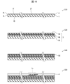
- FIG. 10 is a cross-sectional view showing an example of a method for manufacturing a semiconductor device according to an embodiment of the present disclosure.
- the conductive film 2 does not need to be patterned, and step S20 shown in FIG. 1 may be omitted.
- a base 3 is formed on the upper surface 2T of the conductive film 2 as is.
- FIG. 11 is a cross-sectional view showing an example of a method for manufacturing a display device according to an embodiment of the present disclosure.
- the method for manufacturing a display device according to the present disclosure includes the method for manufacturing a semiconductor device according to the present disclosure, and further includes a step of forming a light-emitting element Ed above the semiconductor device Tr (step S100), and a step of forming a sealing layer 6 for sealing the light-emitting element Ed above the light-emitting element Ed (step S110).
- Steps S60 and S70 are performed after steps S100 and S110.
- a pixel electrode PE is formed above the semiconductor device Tr, an emission layer EM is formed above the pixel electrode PE, and a common electrode CE is formed above the emission layer EM.
- an edge cover film EC that covers the edge of the pixel electrode PE, a charge functional layer located between the pixel electrode PE and the emission layer EM, and a charge functional layer located between the common electrode CE and the emission layer EM may be formed.
- the light-emitting element Ed may be an organic light-emitting diode (OLED) containing an organic light-emitting material in the light-emitting layer EM, or a quantum dot light-emitting diode (QLED) containing light-emitting quantum dots in the light-emitting layer EM.
- OLED organic light-emitting diode
- QLED quantum dot light-emitting diode
- Reference Signs List 1 101 Insulating substrate 1T Upper surface 2 Conductive film 2L Side surface of conductive film 2P Part of conductive film other than outer edge 2S Outer edge of conductive film 2T Upper surface of conductive film 3 Base 4 Backplane 6 Sealing layer BC Base coat Ed Light emitting element ML Intermediate layer R1 First resin layer R2 Second resin layer Tr Semiconductor device UF Upper film
Landscapes
- Devices For Indicating Variable Information By Combining Individual Elements (AREA)
Abstract
本開示に係る半導体装置(Tr)の製造方法は、絶縁性基板(1)の上面(1T)に、導電性膜(2)を形成する工程と、導電性膜(2)の上面(2T)に、樹脂を含む下地(3)を形成する工程と、下地(3)より上層に半導体装置(Tr)を形成する工程と、を含む。
Description
本開示は、半導体装置の製造方法、および表示装置の製造方法に関する。
特許文献1は、ガラス基板上に半導体装置を作製する際に、作製工程の初期段階でガラス基板の下面側に導電性を有する薄膜(例えば、導電性を付与した珪素膜等)を形成することを開示している。
絶縁性基板の上に半導体装置を製造する際に、静電破壊によって欠陥が生じ、半導体装置の製造歩留りが低下する。
本開示に係る半導体装置の製造方法は、絶縁性基板の上面に、導電性膜を形成する工程と、前記導電性膜の上面に、樹脂を含む下地を形成する工程と、前記下地より上層に、半導体装置を形成する工程と、を含む方法である。
本開示に係る表示装置の製造方法は、本開示に係る半導体装置の製造方法を含み、前記半導体装置より上層に、発光素子を形成する工程と、前記発光素子より上層に、前記発光素子を封止する封止層を形成する工程と、をさらに含む方法である。
本開示の一態様によれば、半導体装置または半導体装置を含む表示装置の製造歩留りを向上することができる。
〔実施形態1〕
図1は、本開示の一実施形態に係る半導体装置の製造方法の一例を示す断面図である。図1に示すように、半導体装置の製造方法は、絶縁性基板1の上面1Tに、導電性膜2を形成する工程(ステップS10)と、導電性膜2の上面2Tに樹脂を含む下地3を形成する工程(ステップS30)と、下地3より上層に、半導体装置Trを含むバックプレーン4を形成する工程(ステップS50)とを含む。絶縁性基板1は例えば、ガラス基板である。半導体装置Trは例えば、薄膜トランジスタである。
図1は、本開示の一実施形態に係る半導体装置の製造方法の一例を示す断面図である。図1に示すように、半導体装置の製造方法は、絶縁性基板1の上面1Tに、導電性膜2を形成する工程(ステップS10)と、導電性膜2の上面2Tに樹脂を含む下地3を形成する工程(ステップS30)と、下地3より上層に、半導体装置Trを含むバックプレーン4を形成する工程(ステップS50)とを含む。絶縁性基板1は例えば、ガラス基板である。半導体装置Trは例えば、薄膜トランジスタである。
本開示において、「要素Xの上面に要素Yを形成する」とは、要素Yが要素Xの上面に直接接するように、要素Xよりも後に要素Yを形成することを意味する。「要素Xより上層に要素Yを形成する」とは、要素Xよりも後に要素Yを形成することを意味し、要素Yが要素Xの上面に接する場合も接しない場合も包含する。
図1に示す方法によれば、絶縁性基板1の上面1Tに導電性膜2を形成する。半導体装置の製造の様々な工程で、摩擦によって静電気が生じ、絶縁性基板1に局所的な電荷が生じる。導電性膜2は、局所的な電荷を分散させ、面積あたりの電荷量を低減する。このため、半導体装置Trを含む、導電性膜2より上層に形成される構成要素に対する、面積あたりの電圧負荷が低減される。
図2は、図1に示した方法による電圧負荷の一例を説明する断面図である。簡単化のために、図2および図2を参照する説明では、導電性膜2とバックプレーン4との間の層を無視する。図2に示すように、絶縁性基板1は、ピンまたはアームなどの支持器具STによって支持または搬送される。絶縁性基板1の下面1Bと支持器具STとの間の接触または摩擦によって、静電気が生じ、下面1Bに電荷-Qが生じることがある。このとき、絶縁性基板1の下面1Bの電荷-Qが、上面1Tに電荷+Qを誘起し、絶縁性基板1の上面1Tの電荷+Qが、導電性膜2を介して、バックプレーン4の下面に電荷-Qを誘起する。そして、バックプレーン4の下面の電荷-Qが、上面に電荷+Qを誘起し、バックプレーン4の上面と下面との間に電圧V2が加わる。導電性膜2によって、絶縁性基板1の上面1Tの電荷+Qが分布している面積S1よりも、バックプレーン4の下面の電荷-Qが分布している面積S2は、大きい(S1<S2)。
図3は、比較例の絶縁性基板に導電性膜を形成しない方法による電圧負荷の一例を説明する断面図である。簡単化のために、図3および図3を参照する説明では、絶縁性基板101とバックプレーン104との間の層を無視する。図3に示すように、絶縁性基板101の下面に電荷-Qが生じたとき、絶縁性基板1の下面の電荷-Qが、上面に電荷+Qを誘起し、絶縁性基板101の上面の電荷+Qが、バックプレーン104の下面に電荷-Qを誘起する。そして、バックプレーン104の下面の電荷-Qが、上面に電荷+Qを誘起し、バックプレーン104の上面と下面との間に電圧V1が加わる。導電性膜が無いため、絶縁性基板101の上面の電荷+Qが分布している面積S1と、バックプレーン104の下面の電荷-Qが分布している面積は、同等である。
バックプレーン4,104を平行板コンデンサと見做すことができる。平行板コンデンサに関し、下記の関係式(1)が成立することが知られている。
Q=ε×V×S/d……(1)
ここで、
Q:コンデンサの電極に蓄積されている電荷量の絶対値、
ε:コンデンサの電極間の誘電率、
V:コンデンサの電極間の電圧の絶対値、
S:コンデンサの電極面積、
d:コンデンサの電極間の距離、である。
ここで、
Q:コンデンサの電極に蓄積されている電荷量の絶対値、
ε:コンデンサの電極間の誘電率、
V:コンデンサの電極間の電圧の絶対値、
S:コンデンサの電極面積、
d:コンデンサの電極間の距離、である。
比較例のバックプレーン104の蓄積されている電荷量Q、誘電率εおよび厚さdが、本開示のバックプレーン4の蓄積されている電荷量Q、誘電率εおよび厚さdと同等であるとき、上記関係式(1)に電極間の電圧V1,V2と電極面積S1,S2を適用して関係式(2)を得る。さらに、電極面積S1<S2を適用して関係式(3)を得る。なお、V1,S1,V2,S2は0より大きい。
Q=ε×V1×S1/d=ε×V2×S2/d……(2)
V1>V2……(3)
したがって、比較例の絶縁性基板101に導電性膜を形成しない方法と比較して、本開示に係る方法によれば、半導体装置Trに対する面積あたりの電圧負荷を低減することができる。そして、半導体装置Trの製造歩留りを向上することができる。
V1>V2……(3)
したがって、比較例の絶縁性基板101に導電性膜を形成しない方法と比較して、本開示に係る方法によれば、半導体装置Trに対する面積あたりの電圧負荷を低減することができる。そして、半導体装置Trの製造歩留りを向上することができる。
また、図1に示す方法によれば、絶縁性基板1の上面1Tに導電性膜2を形成し、導電性膜2より上層に下地3およびバックプレーン4を形成する。このため、絶縁性基板1を支持する支持器具STが導電性膜2に接触しない。一方、絶縁性基板の下面に導電性膜を形成し、絶縁性基板より上層に下地およびバックプレーンを形成する方法によれば、絶縁性基板を支持する器具が導電性膜に接触し、導電性膜の一部が剥落することがある。剥落片は異物となり、半導体装置の製造歩留りを低下させる。さらに、絶縁性基板の下面に導電性膜を形成する方法によれば、接触した器具と導電性膜との間で電荷が大規模に移動し、構成要素の静電破壊に繋がる恐れがある。
したがって、絶縁性基板の下面に導電性膜を形成する方法と比較して、本開示に係る方法によれば、バックプレーン4を含む半導体装置の製造歩留りを向上することができる。
図1を再度参照して、導電性膜2を、絶縁性基板1の上面1Tの全体に形成する。本開示に係る半導体装置の製造方法は、導電性膜2を、導電性膜2の外縁部2Sを除去するように、導電性膜2をパターニングする工程(ステップS20)をさらに含む。ステップS30において有益には、下地3がパターニングされた導電性膜2の上面2Tおよび側面2Lを覆うように、下地3を形成する。導電性膜2が下地3によって保護され、導電性膜2の剥落を低減できる。導電性膜2の外縁部2Sは、絶縁性基板1の上面1Tの外縁部の上に形成された部分である。
本開示に係る半導体装置の製造方法は、下地3を形成する工程(ステップS30)において、導電性膜2の上面2Tに第1樹脂層R1を形成し、第1樹脂層R1より上層に中間層MLを形成し、中間層MLより上層に第2樹脂層R2を形成する。第1樹脂層R1を中間層MLで覆うことによって、第1樹脂層R1が吸湿して絶縁性基板1から剥離することを低減できる。第1樹脂層R1および第2樹脂層R2はポリイミドなどの樹脂を含んでよい。中間層MLは、窒化シリコン、酸化シリコンおよび窒酸化シリコンなどの無機材料を含んでよい。
図4は、図1に示した絶縁性基板と、パターニングされた導電性膜と、下地に含まれる樹脂との位置関係の一例を示す平面透視図である。図4に示すように、絶縁性基板1の外周と導電性膜2の外周との間に、下地3に含まれる樹脂の外周が位置する。絶縁性基板1の外周と導電性膜2の外周との間の間隔は、18~19〔mm〕でよい。また、図1を再度参照して、下地3に含まれる第1樹脂層R1は、外縁部で絶縁性基板1に直接接触している。
本開示に係る半導体装置の製造方法は、下地3より上層にベースコートBCを形成する工程(ステップS40)をさらに含み、ベースコートBCより上層に半導体装置Trを形成する。第2樹脂層R2をベースコートBCで覆うことによって、第2樹脂層R2が吸湿して絶縁性基板1から剥離することを低減できる。ベースコートBCは、窒化シリコン、酸化シリコンおよび窒酸化シリコンなどの無機材料を含んでよい。
導電性膜2は、透明金属酸化物を含んでよく、例えば、インジウムスズ酸化物(ITO)、インジウム亜鉛酸化物(IZO)およびインジウムガリウム亜鉛酸化物(InGaZnO)を含む群から選択される1つ以上を含んでよい。あるいは、導電性膜2は、導電性有機物を含んでよく、例えば、カーボンナノチューブ、グラフェン、およびフラーレンを含む群から選択される1つ以上を含んでよい。あるいは、導電性膜2は、導電性を付与する不純物イオンをドープされたシリコン薄膜などの半導体薄膜であってよい。シリコン薄膜に導電性を付与する不純物は、リンイオンまたはボロンイオンを含む。
導電性膜2は、ステップS10よりも後の工程、例えば、半導体装置Trを形成する工程で生じる熱に耐える材料からなる。導電性膜2は、400℃~500℃に耐える耐熱性を有してよい。
導電性膜2は、電気的にフローティング状態であってよい。下地3に開口を設け、この開口を通じて、導電性膜2は、バックプレーン4中の配線層と電気的に接続されてもよい。この電気的接続は、後述する下地3を絶縁性基板1から剥離する工程(ステップS70)によって、分離される。
ステップS10において導電性膜2を、絶縁性基板1の上面1Tの全体に形成する。また、導電性膜2を、絶縁性基板1の上面1Tのみに形成する。絶縁性基板1の下面1Bおよび側面1Lは、非導電性のままであるため、支持器具STが下面1Bまたは側面1Lに接触しても、支持器具STと絶縁性基板1との間で電荷が移動困難である。したがって、支持器具STとの電荷移動に起因する静電破壊を低減することができる。
図5は、図1に示した半導体装置の製造方法の一例の続きを示す断面図である。図5に示すように、半導体装置の製造方法は、絶縁性基板1の下から下地3にレーザを照射する工程(ステップS60)と、下地3を絶縁性基板1から剥離する工程(ステップS70)と、をさらに含む。レーザ照射によって、下地3の樹脂が変性し、剥離し易くなる。このため、絶縁性基板1および導電性膜2は、レーザの透過率が高いことが有益である。例えば、導電性膜2は、レーザの透過率が60%以上であってよい。例えば、絶縁性基板1および導電性膜2は合計で、レーザの透過率が60%以上であってよい。ステップS60で照射するレーザの中心波長は、例えば343〔nm〕である。ステップS70において導電性膜2は概ね、絶縁性基板1に残る。
図6は、本開示の実施例に係る透過率グラフを示す図である。図6において、破線は、参照例としてガラス基板のみの透過率グラフを示す。実線のうち「アニールあり」は、ガラス基板上に42nmの平均厚さを有するITO薄膜を形成し、ITO薄膜を500℃でアニール処理したものについて、ガラス基板およびITO薄膜の合計の透過率グラフを示す。実線のうち「アニールなし」は、ガラス基板上に24~42nmの平均厚さを有するITO薄膜を形成し、ITO薄膜をアニール処理していないものについて、ガラス基板およびITO薄膜の合計の透過率グラフを示す。ITO薄膜の厚みには面内ばらつきがある。図6の縦軸は透過率〔%〕を示し、横軸は波長〔nm〕を示す。
図6に示すように、レーザの中心波長343〔nm〕において、ガラス基板のみの透過率は90%未満であり、ガラス基板およびITO薄膜の合計の透過率は、約54%以上である。「ガラス基板およびITO薄膜の合計の透過率」=「ガラス基板の透過率」×「ITO薄膜の透過率」であり、90%×60%=54%である。これらのため、図6に実線で透過率グラフを示した実施例の何れのITO薄膜も、レーザの透過率が約60%以上である。さらに、レーザの中心波長343〔nm〕において、「アニールあり」の合計の透過率は、「アニールなし」の合計の透過率よりも大きく、60%以上である。したがって、本開示に係る半導体装置の製造方法は、導電性膜2をアニール処理する工程をさらに含むことが有益である。
図7は、図1および図4に示した絶縁性基板の再利用の一例を示す断面図である。図7に示すように、下地3を剥離したあとの絶縁性基板1および導電性膜2を再利用してよい。例えば、ステップS70で、中間層MLおよびベースコートBCなどの不要な膜が絶縁性基板1に残っている場合、絶縁性基板1から不要な膜を除去し(ステップS80)、続いて、ステップS30以後の工程を再度行う。
図8は、図1および図4に示した絶縁性基板の再利用の別の一例を示す断面図である。図8に示すように、下地3を剥離したあとの絶縁性基板1から、絶縁性基板1より上層の上膜UFを除去して、絶縁性基板1を再利用してよい。上膜UFは導電性膜2を含んでよい。例えば、絶縁性基板1から導電性膜2、中間層MLおよびベースコートBCを含む上膜UFを除去し(ステップS90)、続いて、ステップS10以後の工程を再度行う。
(変形例)
図9は、本開示の一実施形態に係る半導体装置の製造方法の一変形例を示す断面図である。図9に示すように、ステップS20において、導電性膜2の外縁部2Sに加えて、導電性膜2の外縁部2S以外の部分の任意の一部2Pも除去するように、導電性膜2をパターニングしてよい。
図9は、本開示の一実施形態に係る半導体装置の製造方法の一変形例を示す断面図である。図9に示すように、ステップS20において、導電性膜2の外縁部2Sに加えて、導電性膜2の外縁部2S以外の部分の任意の一部2Pも除去するように、導電性膜2をパターニングしてよい。
導電性膜2は光の透過および反射に影響する。この影響が、半導体装置の製造に不都合である場合、導電性膜2の一部2Pを適宜除去してよい。例えば、導電性膜2によってアライアメントマークAMが視認困難になる場合、導電性膜2のうちアライアメントマークAMの直上および近傍の部分を除去する。
〔実施形態2〕
本開示の他の実施形態について、以下に説明する。なお、説明の便宜上、上記実施形態にて説明した部材と同じ機能を有する部材については、同じ符号を付記し、その説明を繰り返さない。
本開示の他の実施形態について、以下に説明する。なお、説明の便宜上、上記実施形態にて説明した部材と同じ機能を有する部材については、同じ符号を付記し、その説明を繰り返さない。
図10は、本開示の一実施形態に係る半導体装置の製造方法の一例を示す断面図である。図10に示すように、導電性膜2をパターニングしなくてもよく、図1に示したステップS20を省略してよい。絶縁性基板1の上面1Tの全体に導電性膜2を形成した後、そのまま、導電性膜2の上面2Tに下地3を形成する。
〔実施形態3〕
図11は、本開示の一実施形態に係る表示装置の製造方法の一例を示す断面図である。図11に示すように、本開示に係る表示装置の製造方法は、本開示に係る半導体装置の製造方法を含み、半導体装置Trより上層に発光素子Edを形成する工程(ステップS100)と、発光素子Edより上層に、発光素子Edを封止する封止層6を形成する工程(ステップS110)とをさらに含む。ステップS60およびステップS70は、ステップS100およびステップS110よりも後に行われる。
図11は、本開示の一実施形態に係る表示装置の製造方法の一例を示す断面図である。図11に示すように、本開示に係る表示装置の製造方法は、本開示に係る半導体装置の製造方法を含み、半導体装置Trより上層に発光素子Edを形成する工程(ステップS100)と、発光素子Edより上層に、発光素子Edを封止する封止層6を形成する工程(ステップS110)とをさらに含む。ステップS60およびステップS70は、ステップS100およびステップS110よりも後に行われる。
本開示に係る表示装置の製造方法は、発光素子Edを形成する工程(ステップS100)において、半導体装置Trより上層に画素電極PEを形成し、画素電極PEより上層に発光層EMを形成し、発光層EMより上層に共通電極CEを形成する。また、画素電極PEのエッジを覆うエッジカバー膜EC、画素電極PEと発光層EMとの間に位置する電荷機能層、および共通電極CEと発光層EMとの間に位置する電荷機能層を形成してよい。
発光素子Edは、発光層EMに有機発光材料を含む有機発光ダイオード(OLED)であっても、発光層EMに発光性量子ドットを含む量子ドット発光ダイオード(QLED)であってもよい。
本開示は上述した各実施形態に限定されるものではなく、請求項に示した範囲で種々の変更が可能であり、異なる実施形態にそれぞれ開示された技術的手段を適宜組み合わせて得られる実施形態についても本開示の技術的範囲に含まれる。さらに、各実施形態にそれぞれ開示された技術的手段を組み合わせることにより、新しい技術的特徴を形成することができる。
1、101 絶縁性基板
1T 上面
2 導電性膜
2L 導電性膜の側面
2P 導電性膜の外縁部以外の部分の一部
2S 導電性膜の外縁部
2T 導電性膜の上面
3 下地
4 バックプレーン
6 封止層
BC ベースコート
Ed 発光素子
ML 中間層
R1 第1樹脂層
R2 第2樹脂層
Tr 半導体装置
UF 上膜
1T 上面
2 導電性膜
2L 導電性膜の側面
2P 導電性膜の外縁部以外の部分の一部
2S 導電性膜の外縁部
2T 導電性膜の上面
3 下地
4 バックプレーン
6 封止層
BC ベースコート
Ed 発光素子
ML 中間層
R1 第1樹脂層
R2 第2樹脂層
Tr 半導体装置
UF 上膜
Claims (22)
- 絶縁性基板の上面に、導電性膜を形成する工程と、
前記導電性膜の上面に、樹脂を含む下地を形成する工程と、
前記下地より上層に、半導体装置を形成する工程と、を含む、半導体装置の製造方法。 - 前記導電性膜の外縁部を除去するように、前記導電性膜をパターニングする工程をさらに含む、請求項1に記載の半導体装置の製造方法。
- 前記導電性膜の前記外縁部以外の部分の一部も除去するように、前記導電性膜をパターニングする、請求項2に記載の半導体装置の製造方法。
- 前記下地がパターニングされた前記導電性膜の上面および側面を覆うように、前記下地を形成する、請求項2または3の何れか1項に記載の半導体装置の製造方法。
- 前記導電性膜は、透明金属酸化物を含む、請求項1~4の何れか1項に記載の半導体装置の製造方法。
- 前記導電性膜は、インジウムスズ酸化物、インジウム亜鉛酸化物、およびインジウムガリウム亜鉛酸化物を含む群から選択される1つ以上を含む、請求項5に記載の半導体装置の製造方法。
- 前記導電性膜は、導電性有機物を含む、請求項1~4の何れか1項に記載の半導体装置の製造方法。
- 前記導電性膜は、導電性を付与する不純物イオンをドープされたシリコン薄膜である、請求項1~4の何れか1項に記載の半導体装置の製造方法。
- 前記導電性膜は、前記半導体装置を形成する工程で生じる熱に耐える材料からなる、請求項1~8の何れか1項に記載の半導体装置の製造方法。
- 前記導電性膜は、400℃~500℃の耐熱性を有する、請求項1~9の何れか1項に記載の半導体装置の製造方法。
- 前記導電性膜をアニール処理する工程をさらに含む、請求項1~10の何れか1項に記載の半導体装置の製造方法。
- 前記導電性膜を、前記絶縁性基板の上面のみに形成する、請求項1~11の何れか1項に記載の半導体装置の製造方法。
- 前記絶縁性基板の下から前記下地にレーザを照射する工程と、
前記下地を前記絶縁性基板および前記導電性膜から剥離する工程と、をさらに含む、請求項1~12の何れか1項に記載の半導体装置の製造方法。 - 前記導電性膜は、前記レーザの透過率が60%以上である、請求項13に記載の半導体装置の製造方法。
- 前記絶縁性基板および前記導電性膜は合計で、前記レーザの透過率が60%以上である、請求項14に記載の半導体装置の製造方法。
- 前記下地を剥離した後の前記絶縁性基板から、前記絶縁性基板より上層の上膜を除去する工程と、をさらに含む、請求項13~15の何れか1項に記載の半導体装置の製造方法。
- 前記上膜は、前記導電性膜を含む、請求項16に記載の半導体装置の製造方法。
- 前記絶縁性基板は、ガラス基板である、請求項1~17の何れか1項に記載の半導体装置の製造方法。
- 前記下地を形成する工程において、
前記導電性膜の上面に、第1樹脂層を形成し、
前記第1樹脂層より上層に、中間層を形成し、
前記中間層より上層に、第2樹脂層を形成する、請求項1~18の何れか1項に記載の半導体装置の製造方法。 - 前記第1樹脂層および前記第2樹脂層はポリイミドを含む、請求項19に記載の半導体装置の製造方法。
- 前記下地より上層に、ベースコートを形成する工程をさらに含み、
前記ベースコートより上層に、前記半導体装置を形成する、請求項1~20の何れか1項に記載の半導体装置の製造方法。 - 請求項1~21の何れか1項に記載の半導体装置の製造方法を含み、
前記半導体装置より上層に、発光素子を形成する工程と、
前記発光素子より上層に、前記発光素子を封止する封止層を形成する工程と、
をさらに含む、表示装置の製造方法。
Priority Applications (1)
| Application Number | Priority Date | Filing Date | Title |
|---|---|---|---|
| PCT/JP2023/021567 WO2024252675A1 (ja) | 2023-06-09 | 2023-06-09 | 半導体装置の製造方法、および表示装置の製造方法 |
Applications Claiming Priority (1)
| Application Number | Priority Date | Filing Date | Title |
|---|---|---|---|
| PCT/JP2023/021567 WO2024252675A1 (ja) | 2023-06-09 | 2023-06-09 | 半導体装置の製造方法、および表示装置の製造方法 |
Publications (1)
| Publication Number | Publication Date |
|---|---|
| WO2024252675A1 true WO2024252675A1 (ja) | 2024-12-12 |
Family
ID=93795838
Family Applications (1)
| Application Number | Title | Priority Date | Filing Date |
|---|---|---|---|
| PCT/JP2023/021567 Ceased WO2024252675A1 (ja) | 2023-06-09 | 2023-06-09 | 半導体装置の製造方法、および表示装置の製造方法 |
Country Status (1)
| Country | Link |
|---|---|
| WO (1) | WO2024252675A1 (ja) |
Citations (7)
| Publication number | Priority date | Publication date | Assignee | Title |
|---|---|---|---|---|
| JPH04367268A (ja) * | 1991-06-14 | 1992-12-18 | Nec Corp | 薄膜トランジスタアレイ装置 |
| JPH0688973A (ja) * | 1992-07-21 | 1994-03-29 | Semiconductor Energy Lab Co Ltd | 透明導電膜およびそれを用いた半導体装置ならびにその作製方法 |
| JP2011009704A (ja) * | 2009-05-26 | 2011-01-13 | Seiko Epson Corp | 薄膜装置、薄膜装置を備えた可撓性回路基板、及び薄膜装置の製造方法 |
| JP2011248072A (ja) * | 2010-05-26 | 2011-12-08 | Hitachi Displays Ltd | 画像表示装置の製造方法 |
| WO2012070483A1 (ja) * | 2010-11-25 | 2012-05-31 | シャープ株式会社 | フレキシブルデバイス、その製造方法、および表示装置 |
| JP2019124771A (ja) * | 2018-01-15 | 2019-07-25 | 株式会社ジャパンディスプレイ | 表示装置 |
| JP2019165224A (ja) * | 2018-03-15 | 2019-09-26 | 大日本印刷株式会社 | 配線基板、及び配線基板の製造方法 |
-
2023
- 2023-06-09 WO PCT/JP2023/021567 patent/WO2024252675A1/ja not_active Ceased
Patent Citations (7)
| Publication number | Priority date | Publication date | Assignee | Title |
|---|---|---|---|---|
| JPH04367268A (ja) * | 1991-06-14 | 1992-12-18 | Nec Corp | 薄膜トランジスタアレイ装置 |
| JPH0688973A (ja) * | 1992-07-21 | 1994-03-29 | Semiconductor Energy Lab Co Ltd | 透明導電膜およびそれを用いた半導体装置ならびにその作製方法 |
| JP2011009704A (ja) * | 2009-05-26 | 2011-01-13 | Seiko Epson Corp | 薄膜装置、薄膜装置を備えた可撓性回路基板、及び薄膜装置の製造方法 |
| JP2011248072A (ja) * | 2010-05-26 | 2011-12-08 | Hitachi Displays Ltd | 画像表示装置の製造方法 |
| WO2012070483A1 (ja) * | 2010-11-25 | 2012-05-31 | シャープ株式会社 | フレキシブルデバイス、その製造方法、および表示装置 |
| JP2019124771A (ja) * | 2018-01-15 | 2019-07-25 | 株式会社ジャパンディスプレイ | 表示装置 |
| JP2019165224A (ja) * | 2018-03-15 | 2019-09-26 | 大日本印刷株式会社 | 配線基板、及び配線基板の製造方法 |
Similar Documents
| Publication | Publication Date | Title |
|---|---|---|
| US6958252B2 (en) | Flat panel display device and method of manufacturing the same | |
| CN101431093B (zh) | 有机发光器件及其制造方法 | |
| US11139364B2 (en) | Display panel and method of producing same | |
| CN1196378C (zh) | 有机场致发光器件中的阴极接触结构 | |
| KR101510212B1 (ko) | 산화물 반도체 박막 트랜지스터의 제조방법 | |
| US10873048B2 (en) | Quantum-dot light emitting diode, method of fabricating the quantum-dot light emitting diode and quantum-dot light emitting display device | |
| US20110062460A1 (en) | Organic el light emitting element, manufacturing method thereof, and display device | |
| KR100501707B1 (ko) | 유기전계발광표시장치 | |
| CN102890351A (zh) | 制造柔性显示装置的方法 | |
| CN1525799A (zh) | 电场发光显示装置的激光修复方法 | |
| US20070194303A1 (en) | Method for manufacturing organic light-emitting element, organic light-emitting device and organic EL panel | |
| KR102882350B1 (ko) | 디스플레이 장치 | |
| CN1828924A (zh) | 平板显示器及其制造方法 | |
| CN101740565A (zh) | 薄膜晶体管及其制造方法和有机发光二极管显示装置 | |
| KR100903101B1 (ko) | 유기전계 발광표시장치 및 그의 제조방법 | |
| CN1249649C (zh) | 配线基板及其制造方法 | |
| CN1215567C (zh) | 平板显示器及其制造方法 | |
| CN1450839A (zh) | 电致发光显示装置的制造方法 | |
| KR102452841B1 (ko) | 조명 장치용 플렉서블 oled 패널 및 그 제조 방법 | |
| US7586258B2 (en) | Organic light emitting diode and organic electroluminescent device using the same | |
| US7989240B2 (en) | Methods of manufacturing active matrix substrate and organic light-emitting display device | |
| JP2008108482A (ja) | 有機el表示装置 | |
| CN100565845C (zh) | 像素结构的制作方法 | |
| CN1332448C (zh) | 有源式有机发光二极管的像素结构及其制造方法 | |
| CN1851901A (zh) | 有机发光二极管面板的制作方法 |
Legal Events
| Date | Code | Title | Description |
|---|---|---|---|
| 121 | Ep: the epo has been informed by wipo that ep was designated in this application |
Ref document number: 23940772 Country of ref document: EP Kind code of ref document: A1 |
|
| NENP | Non-entry into the national phase |
Ref country code: DE |