WO2024252774A1 - Condensateur multicouche - Google Patents
Condensateur multicouche Download PDFInfo
- Publication number
- WO2024252774A1 WO2024252774A1 PCT/JP2024/013792 JP2024013792W WO2024252774A1 WO 2024252774 A1 WO2024252774 A1 WO 2024252774A1 JP 2024013792 W JP2024013792 W JP 2024013792W WO 2024252774 A1 WO2024252774 A1 WO 2024252774A1
- Authority
- WO
- WIPO (PCT)
- Prior art keywords
- electrode layer
- internal electrode
- layer
- laminate
- exposed
- Prior art date
- Legal status (The legal status is an assumption and is not a legal conclusion. Google has not performed a legal analysis and makes no representation as to the accuracy of the status listed.)
- Ceased
Links
Images













Classifications
-
- H—ELECTRICITY
- H01—ELECTRIC ELEMENTS
- H01G—CAPACITORS; CAPACITORS, RECTIFIERS, DETECTORS, SWITCHING DEVICES, LIGHT-SENSITIVE OR TEMPERATURE-SENSITIVE DEVICES OF THE ELECTROLYTIC TYPE
- H01G4/00—Fixed capacitors; Processes of their manufacture
- H01G4/002—Details
- H01G4/005—Electrodes
- H01G4/008—Selection of materials
-
- H—ELECTRICITY
- H01—ELECTRIC ELEMENTS
- H01G—CAPACITORS; CAPACITORS, RECTIFIERS, DETECTORS, SWITCHING DEVICES, LIGHT-SENSITIVE OR TEMPERATURE-SENSITIVE DEVICES OF THE ELECTROLYTIC TYPE
- H01G4/00—Fixed capacitors; Processes of their manufacture
- H01G4/002—Details
- H01G4/005—Electrodes
- H01G4/012—Form of non-self-supporting electrodes
-
- H—ELECTRICITY
- H01—ELECTRIC ELEMENTS
- H01G—CAPACITORS; CAPACITORS, RECTIFIERS, DETECTORS, SWITCHING DEVICES, LIGHT-SENSITIVE OR TEMPERATURE-SENSITIVE DEVICES OF THE ELECTROLYTIC TYPE
- H01G4/00—Fixed capacitors; Processes of their manufacture
- H01G4/002—Details
- H01G4/018—Dielectrics
- H01G4/06—Solid dielectrics
- H01G4/14—Organic dielectrics
- H01G4/18—Organic dielectrics of synthetic material, e.g. derivatives of cellulose
-
- H—ELECTRICITY
- H01—ELECTRIC ELEMENTS
- H01G—CAPACITORS; CAPACITORS, RECTIFIERS, DETECTORS, SWITCHING DEVICES, LIGHT-SENSITIVE OR TEMPERATURE-SENSITIVE DEVICES OF THE ELECTROLYTIC TYPE
- H01G4/00—Fixed capacitors; Processes of their manufacture
- H01G4/002—Details
- H01G4/224—Housing; Encapsulation
-
- H—ELECTRICITY
- H01—ELECTRIC ELEMENTS
- H01G—CAPACITORS; CAPACITORS, RECTIFIERS, DETECTORS, SWITCHING DEVICES, LIGHT-SENSITIVE OR TEMPERATURE-SENSITIVE DEVICES OF THE ELECTROLYTIC TYPE
- H01G4/00—Fixed capacitors; Processes of their manufacture
- H01G4/002—Details
- H01G4/228—Terminals
- H01G4/232—Terminals electrically connecting two or more layers of a stacked or rolled capacitor
-
- H—ELECTRICITY
- H01—ELECTRIC ELEMENTS
- H01G—CAPACITORS; CAPACITORS, RECTIFIERS, DETECTORS, SWITCHING DEVICES, LIGHT-SENSITIVE OR TEMPERATURE-SENSITIVE DEVICES OF THE ELECTROLYTIC TYPE
- H01G4/00—Fixed capacitors; Processes of their manufacture
- H01G4/002—Details
- H01G4/228—Terminals
- H01G4/232—Terminals electrically connecting two or more layers of a stacked or rolled capacitor
- H01G4/2325—Terminals electrically connecting two or more layers of a stacked or rolled capacitor characterised by the material of the terminals
-
- H—ELECTRICITY
- H01—ELECTRIC ELEMENTS
- H01G—CAPACITORS; CAPACITORS, RECTIFIERS, DETECTORS, SWITCHING DEVICES, LIGHT-SENSITIVE OR TEMPERATURE-SENSITIVE DEVICES OF THE ELECTROLYTIC TYPE
- H01G4/00—Fixed capacitors; Processes of their manufacture
- H01G4/30—Stacked capacitors
-
- H—ELECTRICITY
- H01—ELECTRIC ELEMENTS
- H01G—CAPACITORS; CAPACITORS, RECTIFIERS, DETECTORS, SWITCHING DEVICES, LIGHT-SENSITIVE OR TEMPERATURE-SENSITIVE DEVICES OF THE ELECTROLYTIC TYPE
- H01G4/00—Fixed capacitors; Processes of their manufacture
- H01G4/32—Wound capacitors
-
- H—ELECTRICITY
- H01—ELECTRIC ELEMENTS
- H01G—CAPACITORS; CAPACITORS, RECTIFIERS, DETECTORS, SWITCHING DEVICES, LIGHT-SENSITIVE OR TEMPERATURE-SENSITIVE DEVICES OF THE ELECTROLYTIC TYPE
- H01G4/00—Fixed capacitors; Processes of their manufacture
- H01G4/33—Thin- or thick-film capacitors (thin- or thick-film circuits; capacitors without a potential-jump or surface barrier specially adapted for integrated circuits, details thereof, multistep manufacturing processes therefor)
Definitions
- the present invention relates to a multilayer capacitor.
- Patent Document 1 discloses a multilayer ceramic capacitor that has a laminate in which dielectric layers and internal electrode layers, the main component of which is ceramic, are alternately stacked, and has a pair of external electrodes.
- the main object of the present invention is to provide a multilayer capacitor with reduced ESR and improved mechanical strength.
- the multilayer capacitor of the present invention comprises a laminate having a first main surface and a second main surface that face each other in a stacking direction, a first side surface and a second side surface that face each other in a width direction perpendicular to the stacking direction, and a first end surface and a second end surface that face each other in a length direction perpendicular to the stacking direction and the width direction, a first external electrode arranged on one or more of the first main surface, second main surface, first side surface, second side surface, first end surface, and second end surface of the laminate, and a second external electrode arranged on one or more of the first main surface, second main surface, first side surface, second side surface, first end surface, and second end surface of the laminate.
- the laminate is characterized by having an inner layer portion including a plurality of inner resin layers stacked in the stacking direction, a first inner electrode layer disposed between two of the inner resin layers and exposed to at least one of the first main surface, the second main surface, the first side surface, the second side surface, the first end surface, and the second end surface, and a second inner electrode layer disposed between two of the inner resin layers and exposed to at least one of the first main surface, the second main surface, the first side surface, the second side surface, the first end surface, and the second end surface.
- the baking process can be performed at a temperature lower than normal, which prevents the metal components of the internal electrode layer from being over-sintered.
- the end of the internal electrode layer regular, i.e., by making the end of the internal electrode layer linear, the current path is shortened and the ESR can be reduced.
- the multilayer capacitor of the present invention can provide a multilayer capacitor with reduced ESR and improved mechanical strength.
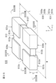
- FIG. 1 is an external perspective view showing a multilayer capacitor according to a first embodiment of the present invention
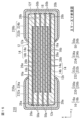
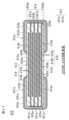
- 2 is a cross-sectional view taken along line II-II in FIG. 1.
- 3 is a cross-sectional view taken along line III-III in FIG. 1.
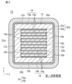
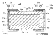
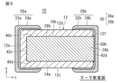
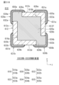
- FIG. 3 is a cross-sectional view taken along line IV-IV in FIG. 3 is a cross-sectional view taken along line VV in FIG. 2.
- 3A is an enlarged view of the ⁇ portion in Fig. 2
- Fig. 3B is an enlarged view of the ⁇ portion in Fig. 2.
- FIG. 5 is a diagram showing measurement points in FIG. 4 .
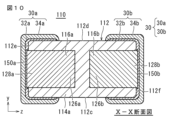
- 2 is a cross-sectional view of a multilayer capacitor according to a second embodiment of the present invention, taken along line II-II in FIG. 1.
- FIG. 3 is a cross-sectional view of the multilayer capacitor according to the second embodiment of the present invention, taken along line III-III in FIG. 1.
- 9 is a cross-sectional view taken along line XX in FIG. 8 .
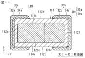
- 10 is a cross-sectional view taken along line XI-XI in FIG. 8.
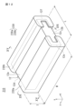
- FIG. 13 is an external perspective view showing a multilayer capacitor in accordance with a third embodiment of the present invention.
- FIG. 13 is a front view showing a multilayer capacitor according to a third embodiment of the present invention.
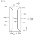
- FIG. 11 is a top view showing a multilayer capacitor according to a third embodiment of the present invention.
- 13 is a cross-sectional view taken along line XV-XV in FIG. 12.
- FIG. 13 is a cross-sectional view taken along line XVI-XVI in FIG. 12.
- FIG. 13 is an exploded perspective view of the laminate shown in FIG. 12 .
- FIG. 13 is an external perspective view showing a multilayer capacitor in accordance with a fourth embodiment of the present invention.
- FIG. 13 is a front view showing a multilayer capacitor according to a fourth embodiment of the present invention.
- FIG. 13 is a top view showing a multilayer capacitor according to a fourth embodiment of the present invention.
- 19 is a cross-sectional view taken along line XXI-XXI in FIG. 18.
- 19 is a cross-sectional view taken along line XXII-XXII in FIG. 18.
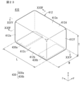
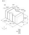
- FIG. 13 is an external perspective view showing a multilayer capacitor in accordance with a fifth embodiment of the present invention.
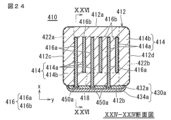
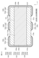
- 24 is a cross-sectional view taken along line XXIV-XXIV in FIG. 23.
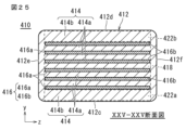
- 24 is a cross-sectional view taken along line XXV-XXV in FIG. 23.
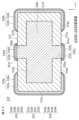
- 25 is a cross-sectional view taken along line XXVI-XXVI in FIG. 24.
- FIG. 24 is an exploded perspective view of the laminate shown in FIG. 23.
- FIG. 13 is an external perspective view showing a multilayer capacitor in accordance with a sixth embodiment of the present invention.
- FIG. 13 is a top view showing a multilayer capacitor in accordance with a sixth embodiment of the present invention.
- FIG. 13 is a front view showing a multilayer capacitor in accordance with a sixth embodiment of the present invention.
- 29 is a cross-sectional view taken along line XXXI-XXXI in FIG. 28.
- 29 is a cross-sectional view taken along line XXXII-XXXII in FIG. 28.
- 32 is a cross-sectional view taken along line XXXIII-XXXIII in FIG. 31 .
- 32 is a cross-sectional view taken along line XXIV-XXXIV in FIG. 31 .
- FIG. 13 is an external perspective view showing a multilayer capacitor in accordance with a seventh embodiment of the present invention.
- FIG. 36 is a cross-sectional view taken along line XXXVI-XXXVI in FIG.
- FIG. 36 is a cross-sectional view taken along line XXXVII-XXXVII in FIG. 35 .
- FIG. 36 is a cross-sectional view taken along line XXXVIII-XXXVIII in FIG. 35 .
- FIG. 36 is an exploded perspective view of the laminate shown in FIG. 35 .
- FIG. 13 is an external perspective view showing a multilayer capacitor in accordance with an eighth embodiment of the present invention. This is a cross-sectional view taken along line XXXI-XXXXI in Figure 40.
- This is a cross-sectional view taken along line XXXII-XXXXII in Figure 40.
- FIG. 41 is an exploded perspective view of the laminate shown in FIG. 40.
- FIG. 1 is an external perspective view showing a multilayer capacitor according to a first embodiment of the present invention.
- FIG. 2 is a cross-sectional view taken along line II-II in FIG. 1.
- FIG. 3 is a cross-sectional view taken along line III-III in FIG. 1.
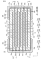
- FIG. 4 is a cross-sectional view taken along line IV-IV in FIG. 2.
- FIG. 5 is a cross-sectional view taken along line V-V in FIG. 2.
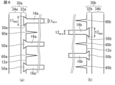
- FIG. 6(a) is an enlarged view of an ⁇ portion in FIG. 2.
- FIG. 6(b) is an enlarged view of a ⁇ portion in FIG. 2.
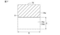
- FIG. 7 is a diagram showing measurement points in FIG. 4.
- the multilayer capacitor 10 has a laminate 12 and an external electrode 30. Below, the configuration of each will be explained in the order of the laminate 12 and the external electrode 30.
- the laminate 12 includes a first main surface 12a and a second main surface 12b facing the stacking direction x, a first side surface 12c and a second side surface 12d facing the width direction y perpendicular to the stacking direction x, and a first end surface 12e and a second end surface 12f facing the length direction z perpendicular to the stacking direction x and the width direction y.
- the first main surface 12a and the second main surface 12b extend along the width direction y and the length direction z, respectively.
- the first side surface 12c and the second side surface 12d extend along the stacking direction x and the length direction z, respectively.
- the first end surface 12e and the second end surface 12f extend along the stacking direction x and the width direction y, respectively.
- the stacking direction x is the direction connecting the first main surface 12a and the second main surface 12b
- the width direction y is the direction connecting the first side surface 12c and the second side surface 12d
- the length direction z is the direction connecting the first end surface 12e and the second end surface 12f.
- the surfaces of the first main surface 12a and the second main surface 12b, the first side surface 12c and the second side surface 12d, and the first end surface 12e and the second end surface 12f may be provided with irregularities, or may be roughened.
- the corners and ridges of the laminate 12 are rounded. Note that a corner refers to a portion where three adjacent faces of the laminate 12 intersect, and a ridge refers to a portion where two adjacent faces of the laminate 12 intersect.
- the laminate 12 includes a plurality of laminated resin layers 14 and a plurality of internal electrode layers 16.
- the resin layers 14 include an inner resin layer 14a and an outer resin layer 14b.
- the internal electrode layers 16 include a first internal electrode layer 16a and a second internal electrode layer 16b.
- the laminate 12 comprises an inner layer 18 and two outer layer sections 20a, 20b arranged to sandwich the inner layer section 18 in the stacking direction x.
- the outer layer section on the first main surface 12a side is referred to as the first main surface side outer layer section 20a
- the outer layer section on the second main surface 12b side is referred to as the second main surface side outer layer section 20b.
- the laminate 12 also comprises two outer layer sections 22a, 22b arranged to sandwich the inner layer section 18 in the width direction y.
- the outer layer section on the first side surface 12c side is referred to as the first side surface side outer layer section 22a
- the outer layer section on the second side surface 12d side is referred to as the second side surface side outer layer section 22b.
- the laminate 12 has an inner layer portion 18 composed of one or more inner resin layers 14a and multiple internal electrode layers 16 arranged thereon.
- the internal electrode layers 16 have a first internal electrode layer 16a that is extended to the first end face 12e and a second internal electrode layer 16b that is extended to the second end face 12f.
- the multiple first internal electrode layers 16a and second internal electrode layers 16b face each other via the inner resin layer 14a.
- the laminate 12 has a first main surface side outer layer portion 20a located on the first main surface 12a side and formed from a plurality of outer layer resin layers 14b located between the first main surface 12a and the outermost surface of the inner layer portion 18 on the first main surface 12a side and a straight line adjacent to that outermost surface.
- the laminate 12 has a second main surface side outer layer portion 20b located on the second main surface 12b side and formed from a plurality of outer layer resin layers 14b located between the second main surface 12b and the outermost surface of the inner layer portion 18 on the second main surface 12b side and a straight line adjacent to that outermost surface.
- the laminate 12 has a first side outer layer portion 22a located on the first side surface 12c side and formed from a plurality of outer resin layers 14b located between the first side surface 12c and the outermost surface of the inner layer portion 18 on the first side surface 12c side.
- the laminate 12 has a second side surface outer layer portion 22b located on the second side surface 12d side and formed from a plurality of outer layer resin layers 14b located between the second side surface 12d and the outermost surface of the inner layer portion 18 on the second side surface 12d side.
- the resin layer 14, i.e., the inner resin layer 14a and the outer resin layer 14b, may be made of, but is not limited to, a liquid crystal polymer (LCP) resin, which has excellent heat resistance, an epoxy resin, or a polyimide resin.
- LCP liquid crystal polymer
- the outer resin layers 14b of the first main surface side outer layer 20a, the second main surface side outer layer 20b, the first side surface side outer layer 22a, and the second side surface side outer layer 22b are each formed from the same type of resin material as the inner resin layer 14a.
- the first main surface side outer layer 20a, the second main surface side outer layer 20b, the first side surface side outer layer 22a, and the second side surface side outer layer 22b may each be composed of multiple outer resin layers 14b or a single outer resin layer 14b.
- the inner resin layer 14a and the outer resin layer 14b can be formed using different components. For example, it is possible to change the inner resin layer 14a to one with a high dielectric constant and the outer resin layer 14b to one with good moisture resistance, weather resistance, and strength resistance.
- the number of inner resin layers 14a and outer resin layers 14b to be laminated is not particularly limited, but it is preferable that the number be 15 or more and 200 or less, including the outer resin layers 14b. In addition, it is preferable that the thickness of the inner resin layer 14a be 0.2 ⁇ m or more and 10.0 ⁇ m or less.
- the internal electrode layer 16 includes a first internal electrode layer 16a and a second internal electrode layer 16b.
- the first internal electrode layer 16a and the second internal electrode layer 16b are alternately stacked with the inner resin layer 14a interposed therebetween. Note that, below, the internal electrode layer may be referred to as the internal electrode.
- the first internal electrode layer 16a is disposed between two of the multiple inner resin layers 14a, and is exposed to at least one of the first main surface 12a, the second main surface 12b, the first side surface 12c, the second side surface 12d, the first end surface 12e, and the second end surface 12f.
- the first internal electrode layer 16a is disposed between two of the inner resin layers 14a, and is exposed to the first end surface 12e.
- the second internal electrode layer 16b is disposed between two of the multiple inner resin layers 14a, and is exposed to at least one of the first main surface 12a, the second main surface 12b, the first side surface 12c, the second side surface 12d, the first end surface 12e, and the second end surface 12f.
- the second internal electrode layer 16b is disposed between two of the inner resin layers 14a, and is exposed to the second end surface 12f.
- the first internal electrode layer 16a is disposed on the surface of the inner resin layer 14a.
- the first internal electrode layer 16a has a first opposing electrode portion 26a that faces the second internal electrode layer 16b, and a first extraction electrode portion 28a that is located on one end side of the first internal electrode layer 16a and extends from the first opposing electrode portion 26a to the first end face 12e of the laminate 12. The end of the first extraction electrode portion 28a is extended to the first end face 12e and exposed.
- the shape of the first opposing electrode portion 26a of the first internal electrode layer 16a is not particularly limited, but is preferably rectangular in plan view. However, the corners in plan view may be rounded or may be formed at an angle in plan view (tapered). It may also be tapered in plan view, with a slope in either direction.
- the shape of the first extraction electrode portion 28a of the first internal electrode layer 16a is not particularly limited, but is preferably rectangular in plan view. However, the corners in plan view may be rounded or may be formed at an angle in plan view (tapered). It may also be tapered in plan view, with a slope in either direction.
- the length in the width direction y of the first opposing electrode portion 26a of the first internal electrode layer 16a and the length in the width direction y of the first extraction electrode portion 28a of the first internal electrode layer 16a may be different, or the length in the width direction y may change toward the first end face 12e side where the first internal electrode layer 16a is exposed.
- the second internal electrode layer 16b is disposed on a surface of an inner resin layer 14a different from the inner resin layer 14a on which the first internal electrode layer 16a is disposed.
- the second internal electrode layer 16b has a second opposing electrode portion 26b that faces the first internal electrode layer 16a, and a second extraction electrode portion 28b that is located on one end side of the second internal electrode layer 16b and extends from the second opposing electrode portion 26b to the second end face 12f of the laminate 12. The end of the second extraction electrode portion 28b is extended to the second end face 12f and exposed.
- the shape of the second opposing electrode portion 26b of the second internal electrode layer 16b is not particularly limited, but is preferably rectangular in plan view. However, the corners in plan view may be rounded or may be formed at an angle in plan view (tapered). It may also be tapered in plan view, with a slope in either direction.
- the shape of the second extraction electrode portion 28b of the second internal electrode layer 16b is not particularly limited, but is preferably rectangular in plan view. However, the corners in plan view may be rounded or may be formed at an angle in plan view (tapered). It may also be tapered in plan view, with a slope in either direction.
- the length in the width direction y of the second opposing electrode portion 26b of the second internal electrode layer 16b and the length in the width direction y of the second extraction electrode portion 28b of the second internal electrode layer 16b may be different, or the length in the width direction y may change toward the second end face 12f side where the second internal electrode layer 16b is exposed.
- the first internal electrode layer 16a and the second internal electrode layer 16b face each other via the inner resin layer 14a, generating capacitance.
- the first internal electrode layer 16a and the second internal electrode layer 16b can be made of an appropriate conductive material, for example, metals such as Ni, Cu, Ag, Pd, Au, or an Ag-Pd alloy that contains one of these metals, but are not limited to these.
- the first internal electrode layer 16a and the second internal electrode layer 16b are made mainly of Cu, which has good conductivity. This can reduce the ESR of the multilayer capacitor 10.
- the dielectric constant of the inner resin layer 14a is lower than that of the dielectric material used in conventional laminated capacitors, the area of the opposing electrode portions 26a, 26b must be increased accordingly to form a capacitor with the same capacitance.
- This requires increasing the number of laminated layers of the first inner electrode layer 16a and the second inner electrode layer 16b.
- the total area of the internal electrode layers 16 increases, and the ESR of the laminated capacitor 10 can be reduced.
- the laminate 12 has the inner resin layer 14a and the outer resin layer 14b, even if the laminated capacitor 10 is deflected, it can be cushioned by the inner resin layer 14a and the outer resin layer 14b, and the deflection strength can be improved. Therefore, the mechanical strength can be improved compared to conventional laminated capacitors.
- the sintering temperature of the dielectric ceramic is higher than that of the internal electrode 16 when the dielectric ceramic is fired, so that over-sintering of the internal electrode 16 may cause the particles to bond together, resulting in voids in the internal electrode 16, which may reduce the effective area and the linearity of the ends of the internal electrode 16.
- the multilayer capacitor 10 can be formed without including a firing process at a temperature exceeding the melting point of the inner resin layer 14a, there is no reduction in the effective area or linearity due to over-sintering of the first internal electrode layer 16a and the second internal electrode layer 16b. Therefore, the area of the internal electrode 16 per unit number can be maximized, and the capacity can be maximized. Furthermore, the linearity of the ends of the internal electrode 16 can be improved, which reduces the ESR.
- the first internal electrode layer 16a and the second internal electrode layer 16b have no voids. This shortens the current path of the multilayer capacitor 10, thereby reducing the ESR.
- the first internal electrode layer 16a has an end 40a in the width direction y on the first side surface 12c side, an end 40b in the width direction y on the second side surface 12d side, an end 42a in the length direction z on the first end surface 12e side, and an end 42b in the length direction z on the second end surface 12f side.
- the end 42a on the first end surface 12e side of the first internal electrode layer 16a is exposed from the laminate 12.
- the end 40a on the first side surface 12c side, the end 40b on the second side surface 12d side, and the end 42b on the second end surface 12f side of the first internal electrode layer 16a are in contact with the inner resin layer 14a.
- the second internal electrode layer 16b has an end 40c in the width direction y on the first side surface 12c side, an end 40d in the width direction y on the second side surface 12d side, an end 42c in the length direction z on the first end surface 12e side, and an end 42d in the length direction z on the second end surface 12f side.
- the end 42d on the second end surface 12f side of the second internal electrode layer 16b is exposed from the laminate 12.
- the end 40c on the first side surface 12c side, the end 40d on the second side surface 12d side, and the end 42c on the first end surface 12e side of the second internal electrode layer 16b are in contact with the inner resin layer 14a.
- the linearity of the end of the first internal electrode layer 16a or the second internal electrode layer 16b where the first internal electrode layer 16a or the second internal electrode layer 16b contacts the inner resin layer 14a is preferably 1.0 or more and 1.5 or less. Furthermore, the linearity of the end of the first internal electrode layer 16a or the second internal electrode layer 16b where the first internal electrode layer 16a or the second internal electrode layer 16b contacts the inner resin layer 14a is preferably 1.0. This allows the current path to be formed as close to the shortest path as possible, thereby reducing the ESR.
- the linearity of the ends 40a, 40b of the first internal electrode layer 16a in the width direction y is calculated by the following method. First, the substrate is polished in the length direction z and width direction y (LW cross section) to expose the first internal electrode layer 16a. Next, a scanning electron microscope (SEM) is used to take an SEM image of the ends 40a, 40b of the first internal electrode layer 16a exposed on the surface in the width direction y at a magnification of 2000 times, centered on 1/2L of the multilayer capacitor 10, and the perimeter, average vertical chord length, and image width are measured.
- Figure 7 is a diagram showing a measurement point 70 in Figure 4.
- the length of the end of the internal electrode layer is A
- the image width is B
- the average vertical chord length is C
- the perimeter is D.
- the perimeter, average vertical chord length, and image width are measured, and the lengths ⁇ A> of the ends 40a, 40b of the first internal electrode layer 16a are calculated by (Equation 1).
- (Equation 1) (End length ⁇ A>) (Circumference length ⁇ D>) - (Average vertical chord length ⁇ C>) x 2 - (Image width ⁇ B>)
- the linearity of the ends 40a, 40b of the first internal electrode layer 16a is calculated using (Equation 2).
- (Equation 2) (Edge Linearity) (Edge Length ⁇ A>)/(Image Width ⁇ B>)
- the linearity of the end portion 42b of the first internal electrode layer 16a in the length direction z is calculated by the following method.
- the substrate is polished in the length direction z and width direction y (LW cross section) to expose the first internal electrode layer 16a.
- a scanning electron microscope (SEM) is used to take an SEM image of the end 42b in the length direction z of the first internal electrode layer 16a exposed on the surface at a magnification of 2000 times, centered on 1/2 W of the multilayer capacitor 10, and the perimeter, average vertical chord length, and image width are measured.
- the length of the end of the internal electrode layer is designated as A, the image width as B, the average vertical chord length as C, and the perimeter as D. From the SEM image, the perimeter, average vertical chord length, and image width are measured, and the linearity of the end 42b in the length direction z of the first internal electrode layer 16a is calculated using the above (Equation 1) and (Equation 2).
- the linearity of the ends 40c, 40d of the second internal electrode layer 16b in the width direction y is calculated by the following method. First, the second internal electrode layer 16b is exposed by polishing in the length direction z and the width direction y (LW cross section). Next, a scanning electron microscope (SEM) is used to take an SEM image of the ends 40c, 40d of the second internal electrode layer 16b in the width direction y exposed on the surface at a magnification of 2000 times centered on 1/2L of the multilayer capacitor 10, and the perimeter, average vertical chord length, and image width are measured.
- the length of the end of the internal electrode layer is A
- the image width is B
- the average vertical chord length is C
- the perimeter is D.
- the perimeter, average vertical chord length, and image width are measured from the SEM image, and the linearity of the ends 40c, 40d of the second internal electrode layer 16b in the width direction y is calculated using the above (Equation 1) and (Equation 2).
- the linearity of the end portion 42c of the second internal electrode layer 16b in the longitudinal direction z is calculated by the following method.
- the second internal electrode layer 16b is exposed by polishing in the length direction z and the width direction y (LW cross section).
- a scanning electron microscope (SEM) is used to take an SEM image of the end 42c in the length direction z of the second internal electrode layer 16b exposed on the surface at a magnification of 2000 times, centered on 1/2W of the multilayer capacitor 10, and the perimeter, average vertical chord length, and image width are measured.
- the length of the end of the internal electrode layer is designated as A, the image width as B, the average vertical chord length as C, and the perimeter as D. From the SEM image, the perimeter, average vertical chord length, and image width are measured, and the linearity of the end 42c in the length direction z of the second internal electrode layer 16b is calculated using the above (Equation 1) and (Equation 2).
- the end 42a on the first end face 12e side which is the end exposed on any one of the first side face 12c, the second side face 12d, the first end face 12e, and the second end face 12f of the laminate 12, of the first internal electrode layer 16a, is thinner in thickness in the stacking direction x toward the face (second end face 12f) opposite to the exposed face of the first internal electrode layer 16a.
- the first internal electrode layer 16a when the first internal electrode layer 16a is exposed on the first end face 12e, the first internal electrode layer 16a is formed in a substantially triangular shape with a shorter length in the stacking direction x from the first end face 12e toward the second end face 12f side in the cross section (LT cross section) in the stacking direction x and the length direction z. This increases the bonding area between the first external electrode 30a and the first internal electrode layer 16a, increasing the adhesion strength and reducing the ESR.
- the end 42a on the first end face 12e side which is the end exposed to any one of the first side face 12c, second side face 12d, first end face 12e and second end face 12f of the laminate 12, among the ends 40a, 40b, 42a, 42b of the first internal electrode layer 16a, is defined as a region where the thickness in the stacking direction x decreases toward the face (second end face 12f) opposite the exposed face of the first internal electrode layer 16a, then it is preferable that the entire first exposed end region 50a is exposed from the laminate 12.
- the end 42a exposed at the first end face 12e of the laminate 12 has a first exposed end region 50a, which is a region in which the thickness in the lamination direction x is reduced toward the second end face 12f opposite the exposed first end face 12e of the first internal electrode layer 16a, and it is preferable that the entire first exposed end region 50a is exposed from the first end face 12e.
- the thickness of the first internal electrode layer 16a in the stacking direction x is defined as the thickest part t1max and the thinnest part t1min .
- the ratio of the thickness of the first internal electrode layer 16a in the stacking direction x between the thickest part t1max and the thinnest part t1min is preferably such that the thickest part t1max is 1.5 times or more and 2.5 times or less than the thinnest part t1min .
- the first exposed end region 50a can be formed, for example, by immersing the first end surface 12e of the laminate 12 in an etching solution and etching the inner resin layer 14a.
- the end 42d on the second end face 12f side which is the end exposed to any one of the first side face 12c, the second side face 12d, the first end face 12e, and the second end face 12f of the laminate 12, has a thickness in the stacking direction x that is thinner toward the face (first end face 12e) opposite to the exposed face of the second internal electrode layer 16b.
- the second internal electrode layer 16b when the second internal electrode layer 16b is exposed to the second end face 12f, the second internal electrode layer 16b is formed to have a substantially triangular shape with a shorter length in the stacking direction x from the second end face 12f toward the first end face 12e side in the cross section (LT cross section) in the stacking direction x and the length direction z.
- This increases the bonding area between the second external electrode 30b and the second internal electrode layer 16b, increasing the adhesion strength and reducing the ESR.
- the second exposed end region 50b which is the region where the thickness in the stacking direction x decreases toward the surface (first end face 12e) opposite the exposed surface of the second internal electrode layer 16b, it is preferable that the entire second exposed end region 50b is exposed from the laminate 12.
- the end 42d exposed at the second end face 12f of the laminate 12 has a second exposed end region 50b, which is a region in which the thickness in the lamination direction x is thinner toward the first end face 12e opposite the exposed second end face 12f of the second internal electrode layer 16b, and it is preferable that the entire second exposed end region 50b is exposed from the second end face 12f.
- the thickness of the second internal electrode layer 16b in the stacking direction x is defined as the thickest part t2max and the thinnest part t2min .
- the ratio of the thickness of the second internal electrode layer 16b in the stacking direction x between the thickest part t2max and the thinnest part t2min is preferably such that the thickest part t2max is 1.5 times or more and 2.5 times or less than the thinnest part t2min .
- the second exposed end region 50b can be formed, for example, by immersing the second end surface 12f of the laminate 12 in an etching solution and etching the inner resin layer 14a.
- the thickness of the stacking direction x of the ends 40a, 40b in the width direction y of the first internal electrode layer 16a thicker than the thickness of the stacking direction x of the center of the width direction y of the first internal electrode layer 16a.
- the total number of the first internal electrode layers 16a and the second internal electrode layers 16b is preferably 15 or more and 200 or less.
- the thickness of the first internal electrode layers 16a and the second internal electrode layers 16b is preferably 1 ⁇ m or more and 12 ⁇ m or less.
- the laminate 12 may have a first cut portion 60a from the first end face 12e where the first internal electrode layer 16a is exposed toward the second end face 12f, which is the opposite face.
- the laminate 12 may have a second cut portion 60b from the second end face 12f where the second internal electrode layer 16b is exposed toward the first end face 12e, which is the opposite face. This allows the external electrode 30 to penetrate into the first cut portion 60a and the second cut portion 60b, and the anchor effect can improve the adhesive strength between the laminate 12 and the external electrode 30.
- the first cut portion 60a and the second cut portion 60b can be formed, for example, by immersing the first end surface 12e and the second end surface 12f of the laminate 12 in an etching solution and etching the inner resin layer 14a.
- the external electrode 30 has a first external electrode 30a and a second external electrode 30b.
- the first external electrode 30a is disposed on one or more of the first main surface 12a, the second main surface 12b, the first side surface 12c, the second side surface 12d, the first end surface 12e, and the second end surface 12f of the laminate 12.
- the first external electrode 30a is connected to the first internal electrode layer 16a, and is disposed so as to extend from the first end surface 12e around the first main surface 12a, the second main surface 12b, the first side surface 12c, and a portion of the second side surface 12d.
- the electrode may be disposed, for example, so as not to extend from the first end surface 12e around the first side surface 12c and the second side surface 12d.
- the second external electrode 30b is disposed on one or more of the first main surface 12a, the second main surface 12b, the first side surface 12c, the second side surface 12d, the first end surface 12e, and the second end surface 12f of the laminate 12.
- the second external electrode 30b is connected to the second internal electrode layer 16b, and is disposed so as to extend from the second end surface 12f around the first main surface 12a, the second main surface 12b, the first side surface 12c, and a part of the second side surface 12d.
- the electrode 30b may be disposed, for example, so as not to extend from the second end surface 12f around the first side surface 12c and the second side surface 12d.
- the external electrode 30 is composed of an underlying electrode layer 32 arranged on at least one of the first principal surface 12a, the second principal surface 12b, the first side surface 12c, the second side surface 12d, the first end surface 12e, and the second end surface 12f, and a plating layer 34 that covers the underlying electrode layer 32.
- the base electrode layer 32 has a first base electrode layer 32a and a second base electrode layer 32b.
- the first base electrode layer 32a is disposed so as to wrap around from the first end face 12e to the first main surface 12a, the second main surface 12b, the first side surface 12c, and a portion of the second side surface 12d.
- the second base electrode layer 32b is disposed so as to wrap around from the second end face 12f to the first main surface 12a, the second main surface 12b, the first side surface 12c, and a portion of the second side surface 12d.
- the base electrode layer 32 includes at least one selected from a baked layer, a conductive resin layer, a thin film layer, etc.
- the baked layer contains a metal component and a glass component.
- the glass component contains at least one selected from B, Si, Ba, Mg, Al, Li, Zn, Ti, etc.
- the metal component of the baked layer contains at least one selected from Cu, Ni, Ag, Pd, Ag-Pd alloy, Au, etc. It is preferable that the metal component of the baked layer is made of a metal such as Cu or Ni. In the case of a baked layer, the metal component acts as a conductive component. Furthermore, the baked layer may be a multi-layered layer.
- the baked layer is formed by applying a conductive paste containing a glass component and a metal component to the laminate 12 and baking it.
- the baked layer may be formed by simultaneously baking a laminated chip having an internal electrode layer 16 and an inner resin layer 14a and a conductive paste applied to the laminated chip, or may be formed by baking a laminated chip having an internal electrode layer 16 and an inner resin layer 14a to obtain the laminate 12, and then applying and baking a conductive paste.
- the baking temperature is preferably lower than the melting point of the inner resin layer 14a. More specifically, the baking temperature is preferably 200°C or lower.
- the thickness in the length direction z connecting the first end face 12e and the second end face 12f of the first baked layer and the second baked layer at the center of the stacking direction x connecting the first main surface 12a and the second main surface 12b of the first baked layer and the second baked layer located at the first end face 12e and the second end face 12f is preferably, for example, 5 ⁇ m or more and 60 ⁇ m or less.
- the thickness in the stacking direction x connecting the first main face 12a and the second main face 12b of the first baked layer and the second baked layer is preferably, for example, 0.5 ⁇ m or more and 20 ⁇ m or less.
- the conductive resin layer includes a thermosetting resin and a metal. Since the conductive resin layer includes a thermosetting resin, it is more flexible than a baked layer made of, for example, a plating film or a baked product of a conductive paste. Therefore, even if the multilayer capacitor 10 is subjected to a physical impact or an impact due to a thermal cycle, the conductive resin layer functions as a buffer layer, and it is possible to further prevent cracks in the multilayer capacitor 10.
- the metal contained in the conductive resin layer can be Ag, Cu, Ni, Sn, Bi, or an alloy containing these. It is also possible to use a metal powder with an Ag coating on the surface. When using a metal powder with an Ag coating on the surface, it is preferable to use Cu, Ni, Sn, Bi, or an alloy powder of these.
- the reason for using Ag conductive metal powder as the conductive metal is that Ag has the lowest resistivity of all metals, making it suitable as an electrode material, and Ag is a precious metal, so it does not oxidize and has high weather resistance. In addition, it is possible to use a cheaper base metal while maintaining the above-mentioned properties of Ag. In the case of a conductive resin layer, the conductive metal acts as the conductive component.
- the metal contained in the conductive resin layer may be Cu or Ni that has been subjected to an anti-oxidation treatment.
- the metal contained in the conductive resin layer may be a metal powder whose surface is coated with Sn, Ni, or Cu.
- Ag, Cu, Ni, Sn, Bi, or an alloy powder of these metals it is preferable to use Ag, Cu, Ni, Sn, Bi, or an alloy powder of these metals.
- the metal contained in the conductive resin layer is mainly responsible for the electrical conductivity of the conductive resin layer. Specifically, when the conductive fillers come into contact with each other, an electrical path is formed inside the conductive resin layer.
- the metal contained in the conductive resin layer can be spherical or flat, but it is preferable to use a mixture of spherical metal powder and flat metal powder.
- thermosetting resins such as epoxy resin, phenolic resin, urethane resin, silicone resin, polyimide resin, etc.
- epoxy resin which has excellent heat resistance, moisture resistance, adhesion, etc., is one of the most suitable resins.
- the conductive resin layer preferably contains a curing agent in addition to the thermosetting resin.
- a curing agent in addition to the thermosetting resin.
- various known compounds such as phenol-based, amine-based, acid anhydride-based, imidazole-based, active ester-based, and amide-imide-based compounds can be used as the curing agent for the epoxy resin.
- the thickest part of the conductive resin layer is preferably, for example, 5 ⁇ m or more and 60 ⁇ m or less.
- the base electrode layer 32 is formed from a thin film layer.
- the thin film layer is formed by a thin film formation method such as a sputtering method or a vapor deposition method.
- the thin film layer is a layer of 1 ⁇ m or less in which metal particles are deposited.
- the base electrode layer 32 may be directly formed by a plating layer.
- the multilayer capacitor 10 may have a structure including a plating layer that is directly electrically connected to the internal electrode layer 16.
- a catalyst may be disposed on the surface of the laminate 12 as a pretreatment, and then the plating layer may be directly formed.
- the plating layer formed as the base electrode layer 32 contains at least one metal selected from, for example, Cu, Ni, Sn, Pb, Au, Ag, Pd, Bi, or Zn, or an alloy containing such a metal.
- the plating layer formed as the base electrode layer 32 does not contain glass. Furthermore, it is preferable that the metal ratio per unit volume of the plating layer formed as the base electrode layer 32 is 99 volume % or more.
- the height can be reduced, i.e., the thickness can be converted to the thickness of the laminate 12, i.e., the thickness of the inner layer 18, thereby improving the design freedom of thin chips.
- the base electrode layer 32 may be formed from one of the above four configurations, or the base electrode layer 32 may be formed from a combination of the above four configurations.
- the plating layer 34 has a first plating layer 34a and a second plating layer 34b.
- the first plating layer 34a is disposed so as to cover the first base electrode layer 32a.
- the second plating layer 34b is disposed so as to cover the second base electrode layer 32b.
- the plating layer 34 includes, for example, at least one selected from Cu, Ni, Sn, Ag, Pd, Ag-Pd alloy, Au, etc.
- the plating layer 34 preferably has at least a two-layer structure.
- Ni plating and Sn plating are arranged in this order from the laminate 12 side.
- Sn plating, Ni plating, and Sn plating are arranged in this order from the laminate 12 side.
- the Ni plating can prevent the base electrode layer 32 from being eroded by solder when mounting the multilayer capacitor 10.
- the Sn plating can improve the wettability of the solder when mounting the multilayer capacitor 10, thereby improving mountability.
- each plating layer 34 is 1 ⁇ m or more and 6 ⁇ m or less.
- the dimension in the length direction z of the multilayer capacitor 10, including the laminate 12, the first external electrode 30a, and the second external electrode 30b, is defined as dimension L
- the dimension in the width direction y of the multilayer capacitor 10, including the laminate 12, the first external electrode 30a, and the second external electrode 30b is defined as dimension W
- the dimension in the stacking direction x of the multilayer capacitor 10, including the laminate 12, the first external electrode 30a, and the second external electrode 30b is defined as dimension T.
- the dimensions of the multilayer capacitor 10 are not limited, but it is preferable that, for example, the L dimension in the length direction z is 0.20 mm or more and 0.65 mm or less, the W dimension in the width direction y is 0.10 mm or more and 0.35 mm or less, and the T dimension in the stacking direction x is 0.01 mm or more and 0.35 mm or less.
- the inner layer 18 of the laminate 12 is formed by alternately stacking a plurality of inner resin layers 14a and a plurality of internal electrode layers 16.
- the baking process can be performed at a temperature lower than usual, and the metal components of the internal electrode layers 16 can be prevented from being over-sintered.
- the generation of voids in the internal electrode layers 16 can be suppressed, and the shape of the ends of the internal electrode layers 16 can be prevented from becoming irregular.
- the ends of the internal electrode layers 16 become regular, i.e., the ends of the internal electrode layers 16 become linear, which shortens the current path and reduces the ESR.
- the inner resin layer 14a and the outer resin layer 14b are resin sheets whose main material is a thermoplastic resin such as liquid crystal polymer (LCP).
- LCP liquid crystal polymer
- a conductor pattern that will become the internal electrode layer 16 is formed on the resin sheets that will become the multiple inner resin layers 14a. More specifically, a metal foil such as Cu foil is laminated on one side of the resin sheets that will become the inner resin layers 14a, and the metal foil is patterned by photolithography and stacked. At this time, for example, the surface of one side of the resin sheet that will become the inner resin layer 14a may be roughened, and Cu foil may be laminated on top of it to improve the adhesive strength between the inner resin layer 14a and the internal electrode layer 16. This forms a block for the inner layer portion. In addition, resin sheets that will become the outer resin layers 14b are stacked to form multiple or single blocks for the first main surface side outer layer portion and multiple or single blocks for the second main surface side outer layer portion.
- the inner layer block is sandwiched between the first main surface side outer layer block and the second main surface side outer layer block, and then heated and pressed (collectively pressed) to produce a laminate block.
- the produced laminate block is cut into individual pieces, for example, by a dicer cut, to form the laminate 12.
- the first end face 12e and the second end face 12f of the laminate 12 may be immersed in an etching solution.
- the inner resin layer 14a is etched, the ends 42a, 42d of the internal electrode layer 16 are exposed, and the first exposed end region 50a and the second exposed end region 50b can be formed.
- a low-temperature curing conductive paste is applied to the first end face 12e and the second end face 12f of the obtained laminate 12, for example by a dipping method, and a baking process is performed at a temperature of 100°C to 250°C to form the base electrode layer 32.
- a dipping method for example by a dipping method
- a baking process is performed at a temperature of 100°C to 250°C to form the base electrode layer 32.
- the conductive paste can also be applied by a screen printing method.
- a conductive resin layer is formed as the base electrode layer 32
- a conductive resin paste containing a thermosetting resin and a metal component is applied to the first end face 12e and the second end face 12f of the obtained laminate 12, and heat treatment is performed at a temperature of 250° C. or less to harden the thermosetting resin to form the base electrode layer 32.
- the heat treatment atmosphere is preferably a N2 atmosphere, and the oxygen concentration is preferably suppressed to 100 ppm or less.
- the base electrode layer 32 can be formed by depositing metal particles on the first end face 12e and the second end face 12f of the obtained laminate 12, for example, by a sputtering method. This allows a thin film of 1.0 ⁇ m or less to be formed as the base electrode layer 32. At this time, by controlling the positional relationship with the laminate 12, such as the angle and distance, it is possible to control the thickness of the base electrode layer 32 and the amount of wrapping around the first main surface 12a, the second main surface 12b, the first side surface 12c, and the second side surface 12d of the laminate 12. In addition, the sputtering method may be applied to each surface individually, not just one surface.
- the first exposed end region 50a and the second exposed end region 50b may cause a step in the base electrode layer 32, and the base electrode layer 32 may be formed discontinuously in the lamination direction x.
- metal particles are deposited from one side, so that the first exposed end region 50a and the second exposed end region 50b may block the metal particles on the surface of each end face 12e, 12f of the laminate 12, resulting in a portion where the metal particles are not deposited, and the thin film layer may not be formed continuously.
- the internal electrode layer 16 and the external electrode 30 are electrically connected by the plating layer 34.
- electrolytic plating When forming a plating layer directly as the base electrode layer 32, electrolytic plating, electroless plating, etc. are used.
- electrolytic plating barrel plating is preferred.
- a plating layer 34 is formed on the formed base electrode layer 32 by, for example, barrel plating.
- the plating layer 34 has a two-layer structure, it is preferable that, for example, Ni plating and Sn plating are arranged in this order from the laminate 12 side.
- the metal types are not limited thereto.
- the plating layer 34 has a three-layer structure, it is preferable that, for example, Sn plating, Ni plating, and Sn plating are arranged in this order from the laminate 12 side.
- the multilayer capacitor 10 according to this embodiment is manufactured.
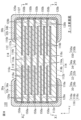
- Fig. 8 is a cross-sectional view of the multilayer capacitor according to the second embodiment of the present invention, taken along line II-II in Fig. 1.
- Fig. 9 is a cross-sectional view of the multilayer capacitor according to the second embodiment of the present invention, taken along line III-III in Fig. 1.
- Fig. 10 is a cross-sectional view taken along line XX in Fig. 8.
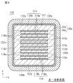
- Fig. 11 is a cross-sectional view taken along line XI-XI in Fig. 8.
- the multilayer capacitor 110 according to the second embodiment has a laminate 112 and an external electrode 30 having a configuration similar to that of the first embodiment.
- the laminate 112 is different from the laminate 12 according to the first embodiment in the structure of the internal electrode layer 116 of the laminate 112. Therefore, the same reference numerals are used for components corresponding to those of the multilayer capacitor 10 according to the first embodiment, and detailed description thereof will be omitted.
- the laminate 112 includes a first main surface 112a and a second main surface 112b facing the stacking direction x, a first side surface 112c and a second side surface 112d facing the width direction y perpendicular to the stacking direction x, and a first end surface 112e and a second end surface 112f facing the length direction z perpendicular to the stacking direction x and the width direction y.
- the first main surface 112a and the second main surface 112b extend along the width direction y and the length direction z, respectively.
- the first side surface 112c and the second side surface 112d extend along the stacking direction x and the length direction z, respectively.
- the first end surface 112e and the second end surface 112f extend along the stacking direction x and the width direction y, respectively. Therefore, the stacking direction x is the direction connecting the first main surface 112a and the second main surface 112b, the width direction y is the direction connecting the first side surface 112c and the second side surface 112d, and the length direction z is the direction connecting the first end surface 112e and the second end surface 112f.
- the surfaces of the first main surface 112a and the second main surface 112b, the first side surface 112c and the second side surface 112d, and the first end surface 112e and the second end surface 112f may be provided with irregularities, or may be roughened.
- the corners and ridges of the laminate 112 are rounded. Note that a corner refers to a portion where three adjacent faces of the laminate 112 intersect, and a ridge refers to a portion where two adjacent faces of the laminate 112 intersect. By rounding the corners and ridges of the laminate 112, chipping or cracking of the laminate 112 can be prevented.
- the laminate 112 includes a plurality of laminated resin layers 114 and a plurality of internal electrode layers 116.
- the resin layer 114 has an inner resin layer 114a and an outer resin layer 114b.
- the internal electrode layer 116 has a first internal electrode layer 116a, a second internal electrode layer 116b, and a floating internal electrode layer 116c.
- the laminate 112 includes an inner layer 118 and two outer layer sections 120a, 120b arranged to sandwich the inner layer section 118 in the stacking direction x.
- the outer layer section on the first main surface 112a side is referred to as the first main surface side outer layer section 120a
- the outer layer section on the second main surface 112b side is referred to as the second main surface side outer layer section 120b.
- the laminate 112 also includes two outer layer sections 122a, 122b arranged to sandwich the inner layer section 118 in the width direction y.
- the outer layer section on the first side surface 112c side is referred to as the first side surface side outer layer section 122a
- the outer layer section on the second side surface 112d side is referred to as the second side surface side outer layer section 122b.
- the laminate 112 has an inner layer section 118 composed of one or more inner resin layers 114a and multiple internal electrode layers 116 arranged thereon.
- the internal electrode layers 116 have a first internal electrode layer 116a that is extended to the first end face 112e and a second internal electrode layer 116b that is extended to the second end face 112f.
- the multiple first internal electrode layers 116a and second internal electrode layers 116b face each other via the inner resin layer 114a.
- the laminate 112 has a first main surface side outer layer portion 120a located on the first main surface 112a side and formed from a plurality of outer layer resin layers 114b located between the first main surface 112a and the outermost surface of the inner layer portion 118 on the first main surface 112a side and a straight line adjacent to that outermost surface.
- the laminate 112 has a second main surface side outer layer portion 120b located on the second main surface 112b side and formed from a plurality of outer layer resin layers 114b located between the second main surface 112b and the outermost surface of the inner layer portion 118 on the second main surface 112b side and a straight line adjacent to that outermost surface.
- the laminate 112 has a first side outer layer portion 122a located on the first side surface 112c side and formed from a plurality of outer resin layers 114b located between the first side surface 112c and the outermost surface of the inner layer portion 118 on the first side surface 112c side.
- the laminate 112 has a second side surface outer layer portion 122b located on the second side surface 112d side and formed from a plurality of outer layer resin layers 114b located between the second side surface 112d and the outermost surface of the inner layer portion 118 on the second side surface 112d side.
- the resin layer 114 i.e., the inner resin layer 114a and the outer resin layer 114b, may be made of, but is not limited to, a liquid crystal polymer (LCP) resin, which has excellent heat resistance, an epoxy resin, or a polyimide resin.
- LCP liquid crystal polymer
- the outer resin layers 114b of the first main surface side outer layer portion 120a, the second main surface side outer layer portion 120b, the first side surface side outer layer portion 122a, and the second side surface side outer layer portion 122b are formed from the same type of resin material as the inner resin layer 114a.
- the first main surface side outer layer portion 120a, the second main surface side outer layer portion 120b, the first side surface side outer layer portion 122a, and the second side surface side outer layer portion 122b may be composed of multiple outer resin layers 114b or may be composed of a single outer resin layer 114b.
- the inner resin layer 114a and the outer resin layer 114b are formed with different components. For example, it is possible to change the inner resin layer 114a to one with a high dielectric constant and the outer resin layer 114b to one with good moisture resistance, weather resistance, and strength resistance.
- the number of inner resin layers 114a and outer resin layers 114b to be stacked is not particularly limited, but it is preferable that the number be 15 or more and 200 or less, including the outer resin layers 114b. In addition, it is preferable that the thickness of the inner resin layer 114a be 0.2 ⁇ m or more and 10.0 ⁇ m or less.
- the internal electrode layer 116 includes a first internal electrode layer 116a, a second internal electrode layer 116b, and a floating internal electrode layer 116c.
- the first internal electrode layer 116a, the second internal electrode layer 116b, and the floating internal electrode layer 116c are alternately stacked with the inner resin layer 114a interposed therebetween.
- the first internal electrode layer 116a is disposed on the surface of the inner resin layer 114a.
- the first internal electrode layer 116a has a first opposing electrode portion 126a that faces the floating internal electrode layer 116c, and a first extraction electrode portion 128a that is located on one end side of the first internal electrode layer 116a and extends from the first opposing electrode portion 126a to the first end face 112e of the laminate 112. The end of the first extraction electrode portion 128a is drawn out to the first end face 112e and exposed.
- the shape of the first opposing electrode portion 126a of the first internal electrode layer 116a is not particularly limited, but is preferably rectangular in plan view. However, the corners in plan view may be rounded or may be formed at an angle in plan view (tapered). It may also be tapered in plan view, with a slope in either direction.
- the shape of the first extraction electrode portion 128a of the first internal electrode layer 116a is not particularly limited, but is preferably rectangular in plan view. However, the corners in plan view may be rounded or the corners may be formed at an angle in plan view (tapered). It may also be tapered in plan view, with a slope in either direction.
- the length in the width direction y of the first opposing electrode portion 126a of the first internal electrode layer 116a and the length in the width direction y of the first extraction electrode portion 128a of the first internal electrode layer 116a may be different, or the length in the width direction y may change toward the first end face 112e side where the first internal electrode layer 116a is exposed.
- the second internal electrode layer 116b is disposed on the surface of the same inner resin layer 114a as the inner resin layer 114a on which the first internal electrode layer 116a is disposed.
- the second internal electrode layer 116b has a second opposing electrode portion 126b that faces the floating internal electrode layer 116c, and a second extraction electrode portion 128b that is located on one end side of the second internal electrode layer 116b and extends from the second opposing electrode portion 126b to the second end surface 112f of the laminate 112. The end of the second extraction electrode portion 128b is extended to the second end surface 112f and exposed.
- the shape of the second opposing electrode portion 126b of the second internal electrode layer 116b is not particularly limited, but is preferably rectangular in plan view. However, the corners in plan view may be rounded or may be formed at an angle in plan view (tapered). It may also be tapered in plan view, with a slope in either direction.
- the shape of the second extraction electrode portion 128b of the second internal electrode layer 116b is not particularly limited, but is preferably rectangular in plan view. However, the corners in plan view may be rounded or may be formed at an angle in plan view (tapered). It may also be tapered in plan view, with a slope in either direction.
- the length in the width direction y of the second opposing electrode portion 126b of the second internal electrode layer 116b and the length in the width direction y of the second extraction electrode portion 128b of the second internal electrode layer 116b may be different, or the length in the width direction y may change toward the second end face 112f side where the second internal electrode layer 116b is exposed.
- the floating internal electrode layer 116c is disposed on a surface of the inner resin layer 114a different from the inner resin layer 114a on which the first internal electrode layer 116a and the second internal electrode layer 116b are disposed.
- the floating internal electrode layer 116c has a third opposing electrode portion 126c facing the first internal electrode layer 116a and a fourth opposing electrode portion 126d facing the second internal electrode layer 116b.
- the third opposing electrode portion 126c and the fourth opposing electrode portion 126d of the floating internal electrode layer 116c are formed so as to be continuous.
- the floating internal electrode layer 116c is not drawn out to either the first end surface 112e or the second end surface 112f. In FIG. 8 and FIG. 11, the third opposing electrode portion 126c and the fourth opposing electrode portion 126d of the floating internal electrode layer 116c are formed so as to be continuous, but may be divided.
- the shapes of the third opposing electrode portion 126c and the fourth opposing electrode portion 126d of the floating internal electrode layer 116c are not particularly limited, but are preferably rectangular in plan view. However, the corners in plan view may be rounded or may be formed at an angle in plan view (tapered). They may also be tapered in plan view, with a slope going in either direction.
- a floating internal electrode layer 116c is provided that is not drawn out to either the first end face 112e or the second end face 112f, and the floating internal electrode layer 116c divides the opposing electrode portion into two (two-unit structure).
- this is not limited to this, and for example, a three-unit structure, a four-unit structure, or a structure with more than four units may also be used.
- the first internal electrode layer 116a, the second internal electrode layer 116b, and the floating internal electrode layer 116c can be made of an appropriate conductive material, for example, metals such as Ni, Cu, Ag, Pd, Au, or an Ag-Pd alloy that contains one of these metals, but is not limited to this.
- the first internal electrode layer 116a, the second internal electrode layer 116b, and the floating internal electrode layer 116c are made mainly of Cu, which has good conductivity. This makes it possible to reduce the ESR of the multilayer capacitor 110.
- the dielectric constant of the inner resin layer 114a is lower than that of the dielectric material used in conventional laminated capacitors, the area of the opposing electrode parts 126a, 126b, 126c, and 126d must be increased accordingly to form a capacitor with the same capacitance. Therefore, it is necessary to increase the number of laminated layers of the first inner electrode layer 116a, the second inner electrode layer 116b, and the floating inner electrode layer 116c. As a result, the total area of the inner electrode layer 116 increases, and the ESR of the laminated capacitor 110 can be reduced.
- the laminate 112 since the laminate 112 has the inner resin layer 114a and the outer resin layer 114b, even if the laminated capacitor 110 is deflected, it can be cushioned by the inner resin layer 114a and the outer resin layer 114b, and the deflection strength can be improved. Therefore, the mechanical strength can be improved compared to conventional laminated capacitors.
- the sintering temperature of the dielectric ceramic is higher than that of the internal electrode 116 when the dielectric ceramic is fired, so that over-sintering of the internal electrode 116 may cause the particles to bond with each other, resulting in voids in the internal electrode 116, which may reduce the effective area and the linearity of the end of the internal electrode 116.
- the multilayer capacitor 110 can be formed without including a firing process at a temperature exceeding the melting point of the inner resin layer 114a, there is no reduction in the effective area or linearity due to over-sintering of the first internal electrode layer 116a, the second internal electrode layer 116b, and the floating internal electrode layer 116c. Therefore, the area of the internal electrode 116 per unit number can be maximized, and the maximum capacity can be obtained. Furthermore, the linearity of the end of the internal electrode 116 can be improved, which reduces the ESR.
- the first internal electrode layer 116a, the second internal electrode layer 116b, and the floating internal electrode layer 116c have no voids. This shortens the current path of the multilayer capacitor 110, thereby reducing the ESR.
- the linearity of the end of the first internal electrode layer 116a or the second internal electrode layer 116b where the first internal electrode layer 116a or the second internal electrode layer 116b contacts the inner resin layer 114a is preferably 1.0 or more and 1.5 or less. Furthermore, the linearity of the end of the first internal electrode layer 116a or the second internal electrode layer 116b where the first internal electrode layer 116a or the second internal electrode layer 116b contacts the inner resin layer 114a is preferably 1.0. This allows the current path to be formed as close to the shortest path as possible, thereby reducing the ESR.
- the linearity of the ends in the width direction y where the first internal electrode layer 116a and the second internal electrode layer 116b contact the inner resin layer 114a can be calculated in the same manner as the linearity of the ends in the width direction y of the internal electrode layer 16 in the first embodiment.
- the linearity of the ends in the length direction z where the first internal electrode layer 116a and the second internal electrode layer 116b contact the inner resin layer 114a can be calculated in the same manner as the linearity of the ends in the length direction z of the internal electrode layer 16 in the first embodiment.
- the end of the first internal electrode layer 116a on the first end face 112e side which is the end exposed to any one of the first side face 112c, the second side face 112d, the first end face 112e, and the second end face 112f of the laminate 112, has a thickness in the stacking direction x that is thinner toward the face (second end face 112f) opposite to the exposed face of the first internal electrode layer 116a.
- the first internal electrode layer 116a when the first internal electrode layer 116a is exposed to the first end face 112e, in a cross section (LT cross section) in the stacking direction x and the length direction z, the first internal electrode layer 116a is formed to have a substantially triangular shape with a short length in the stacking direction x from the first end face 112e toward the second end face 112f side. This increases the bonding area between the first external electrode 30a and the first internal electrode layer 116a, thereby increasing the fixing force and reducing the ESR.
- the first exposed end region 150a is defined as a first exposed end region 150a. It is preferable that the entire first exposed end region 150a is exposed from the laminate 112. By exposing the entire first exposed end region 150a from the laminate 112, the bonding area between the first external electrode 30a and the first internal electrode layer 116a increases, so that the fixing force increases and the ESR decreases.
- the ratio of the thickness of the first internal electrode layer 116a in the stacking direction x between the thickest part and the thinnest part is 1.5 times or more and 2.5 times or less than the thinnest part.
- the first exposed end region 150a can be formed, for example, by immersing the first end surface 112e of the laminate 112 in an etching solution and etching the inner resin layer 114a.
- the end of the second internal electrode layer 116b on the second end face 112f side which is the end exposed to any one of the first side face 112c, the second side face 112d, the first end face 112e, and the second end face 112f of the laminate 112, has a thickness in the stacking direction x that is thinner toward the face (first end face 112e) opposite to the exposed face of the second internal electrode layer 116b.
- the second internal electrode layer 116b when the second internal electrode layer 116b is exposed to the second end face 112f, in a cross section (LT cross section) in the stacking direction x and the length direction z, the second internal electrode layer 116b is formed to have a substantially triangular shape with a short length in the stacking direction x from the second end face 112f toward the first end face 112e side.
- the bonding area between the second external electrode 30b and the second internal electrode layer 116b increases, increasing the fixing force and reducing the ESR.
- the second exposed end region 150b is defined as a region, and it is preferable that the entire second exposed end region 150b is exposed from the laminate 112.
- the ratio of the thickness of the second internal electrode layer 116b in the stacking direction x between the thickest and thinnest parts is preferably 1.5 to 2.5 times the thickness of the thinnest part.
- the second exposed end region 150b can be formed, for example, by immersing the second end surface 112f of the laminate 112 in an etching solution and etching the inner resin layer 114a.
- the thickness in the stacking direction x of the end of the width direction y of the first internal electrode layer 116a thicker than the thickness in the stacking direction x of the center of the width direction y of the first internal electrode layer 116a.
- the total number of first internal electrode layers 116a and second internal electrode layers 116b is preferably 15 to 200 inclusive.
- the total number of floating internal electrode layers 116c is preferably 15 to 200 inclusive.
- the laminate 112 may also have a first cutout from the first end face 112e where the first internal electrode layer 116a is exposed toward the second end face 112f, which is the opposite face. Similarly, the laminate 112 may have a second cutout from the second end face 112f where the second internal electrode layer 116b is exposed toward the first end face 112e, which is the opposite face. This allows the external electrode 30 to penetrate into the first cutout and the second cutout, and the anchor effect can improve the adhesive strength between the laminate 112 and the external electrode 30.
- the first and second cuts can be formed, for example, by immersing the first end surface 112e and the second end surface 112f of the laminate 112 in an etching solution and etching the inner resin layer 114a.
- the method for manufacturing the multilayer capacitor 110 according to the second embodiment is the same as the method for manufacturing the multilayer capacitor 10 according to the first embodiment, except that the first internal electrode layer 116a and the second internal electrode layer 116b are arranged on the same inner resin layer 114a, and the first internal electrode layer 116a and the second internal electrode layer 116b are alternately stacked with the floating internal electrode layer 116c.
- the multilayer capacitor 110 according to the second embodiment which has the above-described configuration, has the same effects as the multilayer capacitor 10 according to the first embodiment, in addition to the effects described above.
- Fig. 12 is an external perspective view of the multilayer capacitor according to the third embodiment of the present invention.
- Fig. 13 is a front view of the multilayer capacitor according to the third embodiment of the present invention.
- Fig. 14 is a top view of the multilayer capacitor according to the third embodiment of the present invention.
- Fig. 15 is a cross-sectional view taken along line XV-XV in Fig. 12.
- Fig. 16 is a cross-sectional view taken along line XVI-XVI in Fig. 12.
- Fig. 17 is an exploded perspective view of the laminate shown in Fig. 12.
- the multilayer capacitor 210 according to the third embodiment has a laminate 12 and an external electrode 230 having the same configuration as the multilayer capacitor 10 according to the first embodiment.
- the L dimension and W dimension of the multilayer capacitor 210 are interchanged with those of the multilayer capacitor 10 according to the first embodiment. Therefore, the same reference numerals are used for components corresponding to those of the multilayer capacitor 10 according to the first embodiment, and detailed description thereof will be omitted.
- external electrodes 230 are arranged on the first end face 12e side and the second end face 12f side of the laminate 12.
- the external electrodes 230 have a first external electrode 230a and a second external electrode 230b.
- the first external electrode 230a is disposed on one or more of the first main surface 12a, the second main surface 12b, the first side surface 12c, the second side surface 12d, the first end surface 12e, and the second end surface 12f of the laminate 12.
- the first external electrode 230a is connected to the first internal electrode layer 16a, and is disposed so as to extend from the first end surface 12e around a portion of the first main surface 12a and the second main surface 12b.
- the second external electrode 230b is disposed on one or more of the first main surface 12a, the second main surface 12b, the first side surface 12c, the second side surface 12d, the first end surface 12e, and the second end surface 12f of the laminate 12.
- the second external electrode 230b is connected to the second internal electrode layer 16b, and is disposed so as to extend from the second end surface 12f around to a portion of the first main surface 12a and the second main surface 12b.
- the first external electrode 230a and the second external electrode 230b each have a U-shape when viewed from the front.
- the external electrode 230 is composed of an underlying electrode layer 232 disposed on at least one of the first principal surface 12a, the second principal surface 12b, the first end surface 12e, and the second end surface 12f, and a plating layer 234 that covers the underlying electrode layer 232.
- the base electrode layer 232 has a first base electrode layer 232a and a second base electrode layer 232b.
- the first base electrode layer 232a is disposed from the first end face 12e around the first principal surface 12a and a part of the second principal surface 12b.
- the second base electrode layer 232b is disposed from the second end face 12f around the first principal surface 12a and a part of the second principal surface 12b.
- the base electrode layer 232 includes at least one selected from a baked layer, a conductive resin layer, a thin film layer, etc.
- the base electrode layer 232 corresponds to the base electrode layer 32 of the first embodiment.
- the material and manufacturing method of the base electrode layer 232 are the same as those of the base electrode layer 32 of the first embodiment, and therefore a description thereof will be omitted.
- the plating layer 234 has a first plating layer 234a and a second plating layer 234b.
- the first plating layer 234a is arranged so as to cover the first base electrode layer 232a.
- the second plating layer 234b is arranged so as to cover the second base electrode layer 232b.
- the plating layer 234 corresponds to the plating layer 34 in the first embodiment.
- the material and manufacturing method of the plating layer 234 are the same as those of the plating layer 34 in the first embodiment, so a description thereof will be omitted.
- the method for manufacturing the multilayer capacitor according to the third embodiment is the same as the method for manufacturing the multilayer capacitor 10 according to the first embodiment.
- the multilayer capacitor 10 according to the first embodiment is manufactured so that the L dimension and the W dimension are interchanged.
- the multilayer capacitor 210 according to the third embodiment which has the above-described configuration, provides the same effects as the multilayer capacitor 10 according to the first embodiment.
- a multilayer capacitor 310 according to a fourth embodiment of the present invention will be described.
- Fig. 18 is an external perspective view of the multilayer capacitor according to the fourth embodiment of the present invention.
- Fig. 19 is a front view of the multilayer capacitor according to the fourth embodiment of the present invention.
- Fig. 20 is a top view of the multilayer capacitor according to the fourth embodiment of the present invention.
- Fig. 21 is a cross-sectional view taken along line XXI-XXI in Fig. 18.
- Fig. 22 is a cross-sectional view taken along line XXII-XXII in Fig. 18.
- the multilayer capacitor 310 according to the fourth embodiment has a laminate 12 and an external electrode 330 having the same configuration as the multilayer capacitor 10 according to the first embodiment.
- the L dimension and W dimension of the multilayer capacitor 310 are interchanged with those of the multilayer capacitor 10 according to the first embodiment. Therefore, the same reference numerals are used for the components corresponding to those of the multilayer capacitor 10 according to the first embodiment, and detailed description thereof will be omitted.
- external electrodes 330 are arranged on the first end face 12e side and the second end face 12f side of the stack 12.
- the external electrodes 330 have a first external electrode 330a and a second external electrode 330b.
- the first external electrode 330a is disposed on one or more of the first main surface 12a, the second main surface 12b, the first side surface 12c, the second side surface 12d, the first end surface 12e, and the second end surface 12f of the laminate 12.
- the first external electrode 330a is connected to the first internal electrode layer 16a, and is disposed so as to extend from the first end surface 12e around to a portion of the first main surface 12a and the second main surface 12b.
- the second external electrode 330b is disposed on one or more of the first main surface 12a, the second main surface 12b, the first side surface 12c, the second side surface 12d, the first end surface 12e, and the second end surface 12f of the laminate 12.
- the second external electrode 330b is connected to the second internal electrode layer 16b, and is disposed so as to extend from the second end surface 12f around to a portion of the first main surface 12a and the second main surface 12b.
- the first external electrode 330a has, on the surface of the first main surface 12a, a first side 336a facing the second external electrode 330b, a second side 337a in contact with the first end face 12e, and a fifth side 338a connecting the first side 336a and the second side 337a on the first side 12c side and the second side 12d side.
- the first external electrode 330a is also formed in a similar manner on the second main surface 12b. Furthermore, the length of the first side 336a of the first external electrode 330a is formed to be shorter than the length of the second side 337a of the first external electrode 330a.
- the second external electrode 330b has a third side 336b facing the first external electrode 330a on the surface of the first main surface 12a, a fourth side 337b in contact with the second end surface 12f, and a sixth side 338b connecting the third side 336b and the fourth side 337b on the first side surface 12c side and the second side surface 12d side.
- the second external electrode 330b is also formed in a similar manner on the second main surface 12b. Furthermore, the length of the third side 336b of the second external electrode 330b is formed to be shorter than the length of the fourth side 337b of the second external electrode 330b.
- the fifth side 338a connecting the first side 336a and the second side 337a of the first external electrode 330a and the sixth side 338b connecting the third side 336b and the fourth side 337b of the second external electrode 330b can reduce or eliminate the area in contact with the ridge where the first main surface 12a and the first side 12c intersect and the ridge where the first main surface 12a and the second side 12d intersect.
- the stress transmitted from the external electrode 330 to the laminate 12 can be reduced. This makes it possible to suppress the occurrence of cracks in the laminate capacitor 310.
- the external electrode 330 is composed of an underlying electrode layer 332 disposed on at least one of the first principal surface 12a, the second principal surface 12b, the first end surface 12e, and the second end surface 12f, and a plating layer 334 that covers the underlying electrode layer 332.
- the shape of the external electrode 330 (underlying electrode layer 332) is controlled by the mask design.
- the base electrode layer 332 has a first base electrode layer 332a and a second base electrode layer 332b.
- the first base electrode layer 332a is disposed from the first end face 12e around the first main surface 12a and a part of the second main surface 12b.
- the second base electrode layer 332b is disposed from the second end face 12f around the first main surface 12a and a part of the second main surface 12b.
- the base electrode layer 332 includes at least one selected from a baked layer, a conductive resin layer, a thin film layer, etc.
- the base electrode layer 332 corresponds to the base electrode layer 32 of the first embodiment.
- the material and manufacturing method of the base electrode layer 332 are the same as those of the base electrode layer 32 of the first embodiment, so a description thereof will be omitted.
- the plating layer 334 has a first plating layer 334a and a second plating layer 334b.
- the first plating layer 334a is disposed so as to cover the first base electrode layer 332a.
- the second plating layer 334b is disposed so as to cover the second base electrode layer 332b.
- the plating layer 334 corresponds to the plating layer 34 in the first embodiment.
- the material and manufacturing method of the plating layer 334 are the same as those of the plating layer 34 in the first embodiment, so a description thereof will be omitted.
- the manufacturing method of the multilayer capacitor 310 according to the fourth embodiment is the same as the manufacturing method of the multilayer capacitor 10 according to the first embodiment.
- the multilayer capacitor 310 according to the fourth embodiment is created so that the L dimension and the W dimension are interchanged compared to the multilayer capacitor 10 according to the first embodiment.
- the shape of the external electrode 330 can be formed by controlling the mask design.
- the multilayer capacitor 310 according to the fourth embodiment which has the above-mentioned configuration, has the same effects as the multilayer capacitor 10 according to the first embodiment, in addition to the above-mentioned effects.
- FIG. 23 is an external perspective view of the multilayer capacitor according to the fifth embodiment of the present invention.
- Fig. 24 is a cross-sectional view taken along line XXIV-XXIV in Fig. 23.
- Fig. 25 is a cross-sectional view taken along line XXV-XXV in Fig. 23.
- Fig. 26 is a cross-sectional view taken along line XXVI-XXVI in Fig. 23.
- Fig. 27 is an exploded perspective view of the multilayer body shown in Fig. 23.
- the multilayer capacitor 410 has a laminate 412 and an external electrode 430.
- the laminate 412 includes a first main surface 412a and a second main surface 412b that face the height direction x, a first side surface 412c and a second side surface 412d that face the width direction y perpendicular to the height direction x, and a first end surface 412e and a second end surface 412f that face the length direction z perpendicular to the height direction x and the width direction y.
- the first main surface 412a and the second main surface 412b extend along the width direction y and the length direction z, respectively.
- the first side surface 412c and the second side surface 412d extend along the height direction x and the length direction z, respectively.
- the first end surface 412e and the second end surface 412f extend along the height direction x and the width direction y, respectively. Therefore, the height direction x is the direction connecting the first main surface 412a and the second main surface 412b, the width direction y is the direction connecting the first side surface 412c and the second side surface 412d, and the length direction z is the direction connecting the first end surface 412e and the second end surface 412f.
- the first main surface 412a and the second main surface 412b are parallel to the surface (mounting surface) on which the stacked capacitor 410 is mounted.
- the laminate 412 includes a plurality of laminated resin layers 414 and a plurality of internal electrode layers 416.
- the resin layers 414 have an inner resin layer 414a and an outer resin layer 414b.
- the internal electrode layers 416 have a first internal electrode layer 416a and a second internal electrode layer 416b.
- the resin layers 414 and the internal electrode layers 416 are laminated in the width direction y.
- the laminate 412 includes an inner layer portion 418 and two outer layer portions 422a, 422b arranged to sandwich the inner layer portion 418 in the width direction y.
- the outer layer portion on the first side surface 412c side is referred to as the first side surface side outer layer portion 422a
- the outer layer portion on the second side surface 412d side is referred to as the second side surface side outer layer portion 422b.
- the laminate 412 has an inner layer section 418 composed of one or more inner resin layers 414a and multiple internal electrode layers 416 arranged thereon.
- the internal electrode layers 416 have a first internal electrode layer 416a that is drawn out to the second main surface 412b on the first end face 412e side, and a second internal electrode layer 416b that is drawn out to the second main surface 412b on the second end face 412f side.
- the multiple first internal electrode layers 416a and second internal electrode layers 416b face each other via the inner resin layer 414a.
- the laminate 412 has a first side surface outer layer portion 422a located on the first side surface 412c side and formed from a plurality of outer resin layers 414b located between the first side surface 412c and the outermost surface of the inner layer portion 418 on the first side surface 412c side and a straight line on that outermost surface.
- the laminate 412 has a second side surface outer layer portion 422b located on the second side surface 412d side and formed from a plurality of outer resin layers 414b located between the second side surface 412d and the outermost surface of the inner layer portion 418 on the second side surface 412d side and a straight line adjacent to that outermost surface.
- the resin layer 414 i.e., the inner resin layer 414a and the outer resin layer 414b, may be made of, but is not limited to, a liquid crystal polymer (LCP) resin, which has excellent heat resistance, an epoxy resin, or a polyimide resin.
- LCP liquid crystal polymer
- the outer resin layer 414b of each of the first side outer layer portion 422a and the second side outer layer portion 422b is formed from the same type of resin material as the inner resin layer 414a.
- the first side outer layer portion 422a and the second side outer layer portion 422b may be composed of multiple outer resin layers 414b or may be composed of a single outer resin layer 414b.
- the inner resin layer 414a and the outer resin layer 414b are also possible to form with different components. For example, it is possible to change the inner resin layer 414a to one with a high dielectric constant and the outer resin layer 414b to one with good moisture resistance, weather resistance, and strength resistance.
- the number of inner resin layers 414a and outer resin layers 414b to be stacked is not particularly limited, but it is preferable that the number be 15 or more and 200 or less, including the outer resin layers 414b. In addition, it is preferable that the thickness of the inner resin layer 414a be 0.2 ⁇ m or more and 10.0 ⁇ m or less.
- the laminate 412 has a plurality of first internal electrode layers 416a and a plurality of second internal electrode layers 416b as the plurality of internal electrode layers 416.
- the first internal electrode layer 416a is disposed on the surface of the inner resin layer 414a.
- the first internal electrode layer 416a also has a first opposing electrode portion 426a that faces the first side surface 412c and the second side surface 412d, and a first extraction electrode portion 428a that extends from the first opposing electrode portion 426a to the second main surface 412b. The end of the first extraction electrode portion 428a is extracted to the second main surface 412b and exposed.
- the second internal electrode layer 416b is disposed on a surface of an inner resin layer 414a different from the inner resin layer 414a on which the first internal electrode layer 416a is disposed.
- the second internal electrode layer 416b has a second opposing electrode portion 426b that faces the first side surface 412c and the second side surface 412d, and a second extraction electrode portion 428b that extends from the second opposing electrode portion 426b to the second main surface 412b.
- the end of the second extraction electrode portion 428b is extended to the second main surface 412b and exposed.
- the first internal electrode layer 416a and the second internal electrode layer 416b are not exposed to the first main surface 412a, both side surfaces 412c and 412d, and both end surfaces 412e and 412f of the laminate 412.
- the first internal electrode layer 416a and the second internal electrode layer 416b have an L-shape.
- the first internal electrode layer 416a and the second internal electrode layer 416b are arranged perpendicular to the first main surface 412a and the second main surface 412b of the laminate 412.
- the first opposing electrode portion 426a of the first internal electrode layer 416a and the second opposing electrode portion 426b of the second internal electrode layer 416b are arranged to face each other.
- the first internal electrode layer 416a and the second internal electrode layer 416b can be made of an appropriate conductive material, for example, metals such as Ni, Cu, Ag, Pd, Au, or an Ag-Pd alloy that contains one of these metals, but are not limited to these.
- the first internal electrode layer 416a and the second internal electrode layer 416b are made mainly of Cu, which has good conductivity. This can reduce the ESR of the multilayer capacitor 410.
- the dielectric constant of the inner resin layer 414a is lower than that of the dielectric material used in conventional laminated capacitors, the area of the opposing electrode parts 426a, 426b must be increased accordingly to form a capacitor with the same capacitance. Therefore, it is necessary to increase the number of laminated layers of the first inner electrode layer 416a and the second inner electrode layer 416b. As a result, the total area of the internal electrode layer 416 increases, and the ESR of the laminated capacitor 410 can be reduced.
- the laminate 412 has the inner resin layer 414a and the outer resin layer 414b, even if the laminated capacitor 410 is deflected, it can be cushioned by the inner resin layer 414a and the outer resin layer 414b, and the deflection strength can be improved. Therefore, the mechanical strength can be improved compared to conventional laminated capacitors.
- the sintering temperature of the dielectric ceramic is higher than that of the internal electrode 416 when the dielectric ceramic is fired, so that over-sintering of the internal electrode 416 bonds the particles together, creating voids in the internal electrode 416, which may reduce the effective area and the linearity of the end of the internal electrode 416.
- the multilayer capacitor 410 can be formed without including a firing process at a temperature exceeding the melting point of the inner resin layer 414a, there is no reduction in the effective area or linearity due to over-sintering of the first internal electrode layer 416a and the second internal electrode layer 416b. Therefore, the area of the internal electrode 416 per unit number can be maximized, and the capacity can be maximized. Furthermore, the linearity of the end of the internal electrode 416 can be improved, which reduces the ESR.
- the first internal electrode layer 416a and the second internal electrode layer 416b have no voids. This shortens the current path of the multilayer capacitor 410, thereby reducing the ESR.
- the linearity of the end of the first internal electrode layer 416a or the second internal electrode layer 416b where the first internal electrode layer 416a or the second internal electrode layer 416b contacts the inner resin layer 414a is preferably 1.0 or more and 1.5 or less. Furthermore, the linearity of the end of the first internal electrode layer 416a or the second internal electrode layer 416b where the first internal electrode layer 416a or the second internal electrode layer 416b contacts the inner resin layer 414a is preferably 1.0. This allows the current path to be formed as close to the shortest path as possible, thereby reducing the ESR.
- the linearity of the end portion of the first internal electrode layer 416a in the height direction x is calculated by the following method.
- the substrate is polished in the length direction z and the height direction x (LT cross section) to expose the first internal electrode layer 416a.
- a scanning electron microscope (SEM) is used to take an SEM image of the end of the first internal electrode layer 416a exposed on the surface in the height direction x at a magnification of 2000 times centered on 1/2L of the multilayer capacitor 410, and the perimeter, average vertical chord length, and image width are measured.
- the length of the end of the internal electrode layer is A
- the image width is B
- the average vertical chord length is C
- the perimeter is D.
- the linearity of the end of the first internal electrode layer 416a in the length direction z is calculated by the following method.
- the substrate is polished in the length direction z and the height direction x (LT cross section) to expose the first internal electrode layer 416a.
- a scanning electron microscope (SEM) is used to take an SEM image of the end of the first internal electrode layer 416a exposed on the surface in the length direction z at a magnification of 2000 times centered on 1/2T of the multilayer capacitor 410, and the perimeter, average vertical chord length, and image width are measured.
- the length of the end of the internal electrode layer is A
- the image width is B
- the average vertical chord length is C
- the perimeter is D.
- From the SEM image the perimeter, average vertical chord length, and image width are measured, and the linearity of the end of the first internal electrode layer 416a in the length direction z is calculated using the above (Equation 1) and (Equation 2).
- the linearity of the end portion of the second internal electrode layer 416b in the height direction x is calculated by the following method.
- the second internal electrode layer 416b is exposed by polishing in the length direction z and the height direction x (LT cross section).
- a scanning electron microscope (SEM) is used to take an SEM image of the end of the second internal electrode layer 416b exposed on the surface in the height direction x at a magnification of 2000 times centered on 1/2L of the multilayer capacitor 410, and the perimeter, average vertical chord length, and image width are measured.
- the length of the end of the internal electrode layer is A
- the image width is B
- the average vertical chord length is C
- the perimeter is D.
- From the SEM image the perimeter, average vertical chord length, and image width are measured, and the linearity of the end of the second internal electrode layer 416b in the height direction x is calculated using the above (Equation 1) and (Equation 2).
- the linearity of the end portion of the second internal electrode layer 416b in the longitudinal direction z is calculated by the following method.
- the second internal electrode layer 416b is exposed by polishing in the length direction z and the height direction x (LT cross section).
- a scanning electron microscope (SEM) is used to take an SEM image of the end of the second internal electrode layer 416b exposed on the surface in the length direction z at a magnification of 2000 times centered on 1/2T of the multilayer capacitor 410, and the perimeter, average vertical chord length, and image width are measured.
- the length of the end of the internal electrode layer is designated as A, the image width as B, the average vertical chord length as C, and the perimeter as D. From the SEM image, the perimeter, average vertical chord length, and image width are measured, and the linearity of the end of the second internal electrode layer 416b in the length direction z is calculated using the above (Equation 1) and (Equation 2).
- the end of the first internal electrode layer 416a on the second main surface 412b side which is the end exposed on one of the surfaces of the laminate 412, is thinner in the stacking direction toward the surface (first main surface 412a) opposite to the exposed surface of the first internal electrode layer 416a.
- the first internal electrode layer 416a when the first internal electrode layer 416a is exposed on the second main surface 412b, in a cross section (WT cross section) in the height direction x and width direction y, the first internal electrode layer 416a is formed to have a substantially triangular shape with a short length in the width direction y (stacking direction in this embodiment) from the second main surface 412b toward the first main surface 412a. This increases the bonding area between the first external electrode 430a and the first internal electrode layer 416a, increasing the fixing force and reducing the ESR.
- the first exposed end region 450a it is preferable that the entire first exposed end region 450a is exposed from the laminate 412. By exposing the entire first exposed end region 450a from the laminate 412, the bonding area between the first external electrode 430a and the first internal electrode layer 416a increases, so that the fixing force increases and the ESR decreases.
- the ratio of the thickness of the first internal electrode layer 416a in the width direction y between the thickest and thinnest parts is 1.5 to 2.5 times the thickness of the thinnest part.
- the first exposed end region 450a can be formed, for example, by immersing the second main surface 412b of the laminate 412 in an etching solution and etching the inner resin layer 414a.
- the end on the second main surface 412b side which is the end exposed to any surface of the laminate 412, becomes thinner in the stacking direction toward the surface (first main surface 412a) opposite to the exposed surface of the second internal electrode layer 416b.
- the second internal electrode layer 416b when the second internal electrode layer 416b is exposed to the second main surface 412b, in a cross section (WT cross section) in the height direction x and width direction y, the second internal electrode layer 416b is formed to have a substantially triangular shape with a short length in the width direction y (stacking direction in this embodiment) from the second main surface 412b toward the first main surface 412a. This increases the bonding area between the second external electrode 430b and the second internal electrode layer 416b, increasing the fixing force and reducing the ESR.
- the second exposed end region 450b is defined as the region where the end of the second internal electrode layer 416b on the second main surface 412b side, which is the end exposed on one of the surfaces of the laminate 412, becomes thinner in the stacking direction toward the surface (first main surface 412a) opposite the exposed surface of the second internal electrode layer 416b, it is preferable that the entire second exposed end region 450b is exposed from the laminate 412. By exposing the entire second exposed end region 450b from the laminate 412, the bonding area between the second external electrode 430b and the second internal electrode layer 416b increases, so that the fixing force increases and the ESR decreases.
- the ratio of the thickness of the second internal electrode layer 416b in the width direction y between the thickest and thinnest parts is 1.5 to 2.5 times the thickness of the thinnest part.
- the second exposed end region 450b can be formed, for example, by immersing the second main surface 412b of the laminate 412 in an etching solution and etching the inner resin layer 414a.
- the thickness in the width direction y of the end of the height direction x of the first internal electrode layer 416a thicker than the thickness in the width direction y of the center of the height direction x of the first internal electrode layer 416a.
- the total number of first internal electrode layers 416a and second internal electrode layers 416b is preferably 15 or more and 200 or less.
- the laminate 412 may also have a notch from the second main surface 412b, where the first internal electrode layer 416a is exposed, toward the first main surface 412a, which is the opposing surface. This allows the external electrode 430 to fit into the notch, and the anchor effect can improve the adhesion between the laminate 412 and the external electrode 430.
- the notch can be formed, for example, by immersing the second main surface 412b of the laminate 412 in an etching solution and etching the inner resin layer 414a.
- An external electrode 430 is formed on the second main surface 412b of the laminate 412.
- the external electrode 430 may be arranged so as to extend from the second main surface 412b around the first side surface 412c and the second side surface 412d.
- the external electrode 430 has a first external electrode 430a electrically connected to the first extraction electrode portion 428a, and a second external electrode 430b electrically connected to the second extraction electrode portion 428b.
- the first opposing electrode portion 426a and the second opposing electrode portion 426b face each other via the inner resin layer 414a, generating electrical characteristics (e.g., capacitance). Therefore, capacitance can be obtained between the first external electrode 430a to which the first internal electrode layer 416a is connected and the second external electrode 430b to which the second internal electrode layer 416b is connected. Therefore, the laminated capacitor 410 having such a structure functions as a capacitor.
- the external electrode 430 has, in order from the laminate 412 side, a base electrode layer 432 and a plating layer 434.
- the base electrode layer 432 has a first base electrode layer 432a and a second base electrode layer 432b.
- the base electrode layer 432 corresponds to the base electrode layer 32 of the multilayer capacitor 10 according to the first embodiment.
- the material and manufacturing method of the base electrode layer 432 are the same as those of the base electrode layer 32 of the first embodiment, and therefore a description thereof will be omitted.
- the plating layer 434 has a first plating layer 434a and a second plating layer 434b.
- the plating layer 434 corresponds to the plating layer 34 of the multilayer capacitor 10 according to the first embodiment.
- the material and manufacturing method of the plating layer 434 are the same as those of the plating layer 34 of the first embodiment, and therefore a description thereof will be omitted.
- the inner resin layer 414a and the outer resin layer 414b are resin sheets whose main material is a thermoplastic resin such as liquid crystal polymer (LCP).
- LCP liquid crystal polymer
- a conductor pattern that will become the internal electrode layer 416 is formed on the resin sheets that will become the multiple inner resin layers 414a. More specifically, a metal foil such as Cu foil is laminated on one side of the resin sheets that will become the inner resin layers 414a, and the metal foil is patterned by photolithography and stacked. At this time, for example, the surface of one side of the resin sheet that will become the inner resin layer 414a may be roughened, and Cu foil may be laminated on top of it to improve the adhesive strength between the inner resin layer 414a and the internal electrode layer 416. This forms a block for the inner layer portion. In addition, resin sheets that will become the outer resin layers 414b are stacked to form multiple or single blocks for the first side outer layer portion and multiple or single blocks for the second side outer layer portion.
- the inner layer block is sandwiched between the first side outer layer block and the second side outer layer block, and then heated and pressed (collectively pressed) to produce a laminate block.
- the produced laminate block is cut into individual pieces, for example, with a dicer, to form the laminate 412.
- the second main surface 412b of the laminate 412 may be immersed in an etching solution. In this way, the inner resin layer 414a is etched, the ends of the internal electrode layer 416 are exposed, and the first exposed end region 450a and the second exposed end region 450b can be formed.
- a low-temperature curing conductive paste is applied to the second main surface 412b of the obtained laminate 412, and a baking process is performed at a temperature of 100°C to 250°C to form the base electrode layer 432.
- Various methods can be used to apply the low-temperature curing conductive paste. For example, a method can be used in which the conductive paste is extruded from a slit and applied to the second main surface 412b of the obtained laminate 412.
- the base electrode layer 432 can be formed not only on the second main surface 412b but also on a part of the first side surface 412c and a part of the second side surface 412d.
- the base electrode layer 432 can also be formed using a roller transfer method.
- the pressing pressure during roller transfer can be increased to form the base electrode layer 432 on a part of the first side surface 412c and a part of the second side surface 412d.
- the conductive paste can also be applied by a screen printing method.
- a conductive resin layer is formed as the base electrode layer 432
- a conductive resin paste containing a thermosetting resin and a metal component is applied to the second main surface 412b of the obtained laminate 412, and heat treatment is performed at a temperature of 250° C. or less to harden the thermosetting resin to form the base electrode layer 432.
- the heat treatment atmosphere is preferably a N2 atmosphere, and the oxygen concentration is preferably suppressed to 100 ppm or less.
- the base electrode layer 432 can be formed by depositing metal particles on the second main surface 412b of the obtained laminate 412, for example, by a sputtering method. This allows a thin film of 1.0 ⁇ m or less to be formed as the base electrode layer 432. At this time, by controlling the positional relationship with the laminate 412, such as the angle and distance, it is possible to control the thickness of the base electrode layer 432 and the amount of wrapping around the first side surface 412c and the second side surface 412d of the laminate 412. Also, sputtering may be performed on each surface individually, not just one surface.
- electrolytic plating When forming a plating layer directly as the base electrode layer 432, electrolytic plating, electroless plating, etc. are used.
- electrolytic plating barrel plating is preferred.
- a plating layer 434 is formed on the formed base electrode layer 432 by, for example, barrel plating.
- the plating layer 434 has a two-layer structure, it is preferable that, for example, Ni plating and Sn plating are arranged in this order from the laminate 412 side.
- the metal types are not limited to this.
- the plating layer 434 has a three-layer structure, it is preferable that, for example, Sn plating, Ni plating, and Sn plating are arranged in this order from the laminate 412 side.
- the multilayer capacitor 410 according to this embodiment is manufactured.
- FIG. 28 is an external perspective view of the multilayer capacitor according to the sixth embodiment of the present invention.
- FIG. 29 is a top view of the multilayer capacitor according to the sixth embodiment of the present invention.
- FIG. 30 is a front view of the multilayer capacitor according to the sixth embodiment of the present invention.
- FIG. 31 is a cross-sectional view taken along line XXXI-XXXI in FIG. 28.
- FIG. 32 is a cross-sectional view taken along line XXXII-XXXII in FIG. 28.
- FIG. 33 is a cross-sectional view taken along line XXXIII-XXXIII in FIG. 31.
- FIG. 34 is a cross-sectional view taken along line XXIV-XXXIV in FIG. 31.
- the stacked capacitor 510 includes a stack 512 and four external electrodes 530.
- the laminate 512 has a first main surface 512a and a second main surface 512b facing the stacking direction x, a first side surface 512c and a second side surface 512d facing the width direction y perpendicular to the stacking direction x, and a first end surface 512e and a second end surface 512f facing the length direction z perpendicular to the stacking direction x and the width direction y.
- the first main surface 512a and the second main surface 512b extend along the width direction y and the length direction z, respectively.
- the first side surface 512c and the second side surface 512d extend along the stacking direction x and the length direction z, respectively.
- the first end surface 512e and the second end surface 512f extend along the stacking direction x and the width direction y, respectively. Therefore, the stacking direction x is the direction connecting the first main surface 512a and the second main surface 512b, the width direction y is the direction connecting the first side surface 512c and the second side surface 512d, and the length direction z is the direction connecting the first end surface 512e and the second end surface 512f.
- the surfaces of the first main surface 512a and the second main surface 512b, the first side surface 512c and the second side surface 512d, and the first end surface 512e and the second end surface 512f may be provided with irregularities, or may be roughened.
- the corners and ridges of the laminate 512 are rounded. Note that a corner refers to a portion where three adjacent faces of the laminate 512 intersect, and a ridge refers to a portion where two adjacent faces of the laminate 512 intersect. By rounding the corners and ridges of the laminate 512, chipping or cracking of the laminate 512 can be prevented.
- the laminate 512 includes a plurality of laminated resin layers 514 and a plurality of internal electrode layers 516.
- the resin layers 514 include an inner resin layer 514a and an outer resin layer 514b.
- the internal electrode layers 516 include a first internal electrode layer 516a and a second internal electrode layer 516b.
- the laminate 512 includes an inner layer portion 518 and two outer layer portions 520a, 520b arranged to sandwich the inner layer portion 518 in the stacking direction x.
- the outer layer portion on the first main surface 512a side is referred to as the first main surface side outer layer portion 520a
- the outer layer portion on the second main surface 512b side is referred to as the second main surface side outer layer portion 520b.
- the laminate 512 has a first main surface side outer layer portion 520a located on the first main surface 512a side and formed from a plurality of outer resin layers 514b located between the first main surface 512a and the outermost surface of the inner layer portion 518 on the first main surface 512a side and a straight line adjacent to that outermost surface.
- the laminate 512 has a second main surface side outer layer portion 520b located on the second main surface 512b side and formed from a plurality of outer resin layers 514b located between the second main surface 512b and the outermost surface of the inner layer portion 518 on the second main surface 512b side and a straight line adjacent to that outermost surface.
- the inner layer portion 518 has a first internal electrode layer 516a having one end exposed on the first end face 512e and the second end face 512f, a second internal electrode layer 516b having one end exposed on the first side face 512c and the second side face 512d, and an inner resin layer 514a laminated alternately with the internal electrode layer 516.
- the resin layer 514 i.e., the inner resin layer 514a and the outer resin layer 514b, may be made of, but is not limited to, a liquid crystal polymer (LCP) resin, which has excellent heat resistance, an epoxy resin, or a polyimide resin.
- LCP liquid crystal polymer
- the outer resin layer 514b of each of the first main surface side outer layer portion 520a and the second main surface side outer layer portion 520b is formed from the same type of resin material as the inner resin layer 514a.
- the first main surface side outer layer portion 520a and the second main surface side outer layer portion 520b may be composed of multiple outer resin layers 514b or may be composed of a single outer resin layer 514b.
- the inner resin layer 514a and the outer resin layer 514b are also possible to form with different components. For example, it is possible to change the inner resin layer 514a to one with a high dielectric constant and the outer resin layer 514b to one with good moisture resistance, weather resistance, and strength resistance.
- the number of inner resin layers 514a and outer resin layers 514b to be stacked is not particularly limited, but it is preferable that the number be 15 or more and 200 or less, including the outer resin layers 514b. In addition, it is preferable that the thickness of the inner resin layer 514a be 0.2 ⁇ m or more and 10.0 ⁇ m or less.
- the internal electrode layer 516 includes a first internal electrode layer 516a and a second internal electrode layer 516b.
- the first internal electrode layer 516a and the second internal electrode layer 516b are alternately stacked with the inner resin layer 514a interposed therebetween.
- the first internal electrode layer 516a is disposed on the surface of the inner resin layer 514a.
- the first internal electrode layer 516a has a first opposing electrode portion 526a located inside the laminate 512, a first extraction electrode portion 528a connected to the first opposing electrode portion 526a and extracted to the first end face 512e, and a second extraction electrode portion 528b extracted to the second end face 512f.
- the shape of the first opposing electrode portion 526a of the first internal electrode layer 516a is not particularly limited, but is preferably rectangular in plan view. However, the corners in plan view may be rounded or may be formed at an angle in plan view (tapered). It may also be tapered in plan view, with a slope in either direction.
- the shape of the first lead electrode portion 528a and the second lead electrode portion 528b of the first internal electrode layer 516a is not particularly limited, but is preferably rectangular in plan view. However, the corners in plan view may be rounded or may be formed at an angle in plan view (tapered). Also, the shape may be tapered in plan view with a slope in either direction.
- the second internal electrode layer 516b is disposed on a surface of an inner resin layer 514a different from the inner resin layer 514a on which the first internal electrode layer 516a is disposed.
- the second internal electrode layer 516b has a second opposing electrode portion 526b that faces the first internal electrode layer 516a, a third extraction electrode portion 529a that is connected to the second opposing electrode portion 526b and is extended to the first side surface 512c, and a fourth extraction electrode portion 529b that is extended to the second side surface 512d.
- the shape of the second opposing electrode portion 526b of the second internal electrode layer 516b is not particularly limited, but is preferably rectangular in plan view. However, the corners in plan view may be rounded or may be formed at an angle in plan view (tapered). It may also be tapered in plan view, with a slope in either direction.
- the shapes of the third extraction electrode portion 529a and the fourth extraction electrode portion 529b of the second internal electrode layer 516b are not particularly limited, but are preferably rectangular in plan view. However, the corners in plan view may be rounded or may be formed at an angle in plan view (tapered). Also, they may be tapered in plan view with a slope in either direction.
- the first opposing electrode portion 526a of the first internal electrode layer 516a and the second opposing electrode portion 526b of the second internal electrode layer 516b face each other via the inner resin layer 514a, forming capacitance and exhibiting the characteristics of a capacitor.
- the first internal electrode layer 516a and the second internal electrode layer 516b can be made of an appropriate conductive material, for example, metals such as Ni, Cu, Ag, Pd, Au, or an Ag-Pd alloy that contains one of these metals, but are not limited to these.
- the first internal electrode layer 516a and the second internal electrode layer 516b are made mainly of Cu, which has good conductivity. This can reduce the ESR of the multilayer capacitor 510.
- the dielectric constant of the inner resin layer 514a is lower than that of the dielectric material used in conventional laminated capacitors, the area of the opposing electrode parts 526a, 526b must be increased accordingly to form a capacitor with the same capacitance. Therefore, it is necessary to increase the number of laminated layers of the first inner electrode layer 516a and the second inner electrode layer 516b. As a result, the total area of the internal electrode layer 516 increases, and the ESR of the laminated capacitor 510 can be reduced.
- the laminate 512 has the inner resin layer 514a and the outer resin layer 514b, even if the laminated capacitor 510 is deflected, it can be cushioned by the inner resin layer 514a and the outer resin layer 514b, and the deflection strength can be improved. Therefore, the mechanical strength can be improved compared to conventional laminated capacitors.
- the sintering temperature of the dielectric ceramic is higher than that of the internal electrode 516 when the dielectric ceramic is fired, so that over-sintering of the internal electrode 516 bonds the particles together, creating voids in the internal electrode 516, which may reduce the effective area and the linearity of the end of the internal electrode 516.
- the multilayer capacitor 510 can be formed without including a firing process at a temperature exceeding the melting point of the inner resin layer 514a, there is no reduction in the effective area or linearity due to over-sintering of the first internal electrode layer 516a and the second internal electrode layer 516b. Therefore, the area of the internal electrode 516 per unit number can be maximized, and the capacity can be maximized. Furthermore, the linearity of the end of the internal electrode 516 can be improved, thereby reducing the ESR.
- the first internal electrode layer 516a and the second internal electrode layer 516b have no voids. This shortens the current path of the multilayer capacitor 510, thereby reducing the ESR.
- the linearity of the end of the first internal electrode layer 516a or the second internal electrode layer 516b where the first internal electrode layer 516a or the second internal electrode layer 516b contacts the inner resin layer 514a is preferably 1.0 or more and 1.5 or less. Furthermore, the linearity of the end of the first internal electrode layer 516a or the second internal electrode layer 516b where the first internal electrode layer 516a or the second internal electrode layer 516b contacts the inner resin layer 514a is preferably 1.0. This allows the current path to be formed as close to the shortest path as possible, thereby reducing the ESR.
- the linearity of the end in the width direction y where the first internal electrode layer 516a contacts the inner resin layer 514a can be calculated in the same manner as the linearity of the end in the width direction y of the internal electrode layer 16 in the first embodiment.
- the linearity of the end in the width direction y where the second internal electrode layer 516b contacts the inner resin layer 514a can be calculated in the same manner as the linearity of the end in the width direction y of the internal electrode layer 16 in the first embodiment, but the measurement point is centered on 1/4L of the multilayer capacitor 510, and an SEM image is taken at a magnification of 2000 times to measure the perimeter, average vertical chord length, and image width.
- the linearity of the end in the length direction z where the second internal electrode layer 516b contacts the inner resin layer 514a can be calculated in a manner similar to the method for calculating the linearity of the end in the length direction z of the internal electrode layer 16 in the first embodiment.
- the end of the first internal electrode layer 516a on the side of the first end face 512e which is the end exposed to any one of the first side face 512c, the second side face 512d, the first end face 512e, and the second end face 512f of the laminate 512, is thinner in the stacking direction x toward the face (second end face 512f) opposite the exposed face of the first internal electrode layer 516a.
- the end of the first internal electrode layer 516a on the side of the second end face 512f which is the end exposed to any one of the first side face 512c, the second side face 512d, the first end face 512e, and the second end face 512f of the laminate 512, is thinner in the stacking direction x toward the face (first end face 512e) opposite the exposed face of the first internal electrode layer 516a.
- the first internal electrode layer 516a is exposed to the first end face 512e and the second end face 512f, and in a cross section (LT cross section) in the stacking direction x and the length direction z, the portion of the first internal electrode layer 516a exposed to the first end face 512e is formed to have a substantially triangular shape with a short length in the stacking direction x from the first end face 512e to the second end face 512f, and the portion of the first internal electrode layer 516a exposed to the second end face 512f is formed to have a substantially triangular shape with a short length in the stacking direction x from the second end face 512f to the first end face 512e.
- the bonding area between the first external electrode 530a and the second external electrode 530b and the first internal electrode layer 516a is increased, so that the fixing force is increased and the ESR is reduced.
- the end of the first internal electrode layer 516a which is the end exposed to any one of the first side surface 512c, the second side surface 512d, the first end surface 512e, and the second end surface 512f of the laminate 512, is a region where the thickness in the stacking direction x decreases toward the surface (second end surface 512f) opposite the exposed surface of the first internal electrode layer 516a, then it is preferable that the entire first exposed end region 550a is exposed from the laminate 512.
- the second exposed end region 550b is preferably exposed in its entirety from the laminate 512.
- the bonding area between the first external electrode 530a and the second external electrode 530b and the first internal electrode layer 516a increases, so that the fixing force increases and the ESR decreases.
- the ratio of the thickness of the first internal electrode layer 516a in the stacking direction x between the thickest part and the thinnest part is 1.5 times or more and 2.5 times or less than the thinnest part.
- the first exposed end region 550a and the second exposed end region 550b can be formed, for example, by immersing the first end face 512e and the second end face 512f of the laminate 512 in an etching solution and etching the inner resin layer 514a.
- the end of the second internal electrode layer 516b on the first side 512c side which is an end exposed to any one of the first side 512c, second side 512d, first end face 512e, and second end face 512f of the laminate 512, is thinner in the stacking direction x toward the face (second side 512d) opposite the exposed face of the second internal electrode layer 516b.
- the end of the second internal electrode layer 516b on the second side 512d side which is an end exposed to any one of the first side 512c, second side 512d, first end face 512e, and second end face 512f of the laminate 512, is thinner in the stacking direction x toward the face (first side 512c) opposite the exposed face of the second internal electrode layer 516b.
- the second internal electrode layer 516b is exposed to the first side 512c and the second side 512d, and in a cross section (WT cross section) in the stacking direction x and the width direction y, the portion of the second internal electrode layer 516b exposed to the first side 512c is formed to have a substantially triangular shape with a short length in the stacking direction x from the first side 512c to the second side 512d, and the portion of the second internal electrode layer 516b exposed to the second side 512d is formed to have a substantially triangular shape with a short length in the stacking direction x from the second side 512d to the first side 512c.
- the bonding area between the third external electrode 530c and the fourth external electrode 530d and the second internal electrode layer 516b is increased, so that the fixing force is increased and the ESR is reduced.
- the end of the second internal electrode layer 516b which is an end exposed to any one of the first side surface 512c, the second side surface 512d, the first end surface 512e, and the second end surface 512f of the laminate 512, is located on the first side surface 512c side, the thickness of which decreases in the stacking direction x toward the surface (second side surface 512d) opposite the exposed surface of the second internal electrode layer 516b, is defined as a third exposed end region 551a, and it is preferable that the entire third exposed end region 551a is exposed from the laminate 512.
- the fourth exposed end region 551b is preferably exposed in its entirety from the laminate 512.
- the bonding area between the third external electrode 530c and the fourth external electrode 530d and the second internal electrode layer 516b increases, so that the fixing force increases and the ESR decreases.
- the ratio of the thickness of the second internal electrode layer 516b in the stacking direction x between the thickest part and the thinnest part is 1.5 times or more and 2.5 times or less than the thinnest part.
- the third exposed end region 551a and the fourth exposed end region 551b can be formed, for example, by immersing the first side 512c and the second side 512d of the laminate 512 in an etching solution and etching the inner resin layer 514a.
- the thickness in the stacking direction x of the end of the width direction y of the first internal electrode layer 516a thicker than the thickness in the stacking direction x of the center of the width direction y of the first internal electrode layer 516a.
- the total number of first internal electrode layers 516a and second internal electrode layers 516b is preferably 15 or more and 200 or less.
- the laminate 512 may have a first cutout from the first end face 512e where the first internal electrode layer 516a is exposed toward the second end face 512f, which is the opposite face. Similarly, the laminate 512 may have a second cutout from the second end face 512f where the first internal electrode layer 516a is exposed toward the first end face 512e, which is the opposite face. Furthermore, the laminate 512 may have a third cut portion provided from the first side surface 512c on which the second internal electrode layer 516b is exposed toward the second side surface 512d, which is the surface facing the first side surface 512c.
- the laminate 512 may have a fourth cut portion provided from the second side surface 512d on which the second internal electrode layer 516b is exposed toward the first side surface 512c, which is the surface facing the second side surface 512d. This allows the external electrode 530 to penetrate into the first cut portion, the second cut portion, the third cut portion, and the fourth cut portion, and the anchor effect can improve the adhesion between the laminate 512 and the external electrode 530.
- the first cut portion, the second cut portion, the third cut portion, and the fourth cut portion can be formed, for example, by immersing the first side surface 512c, the second side surface 512d, the first end surface 512e, and the second end surface 512f of the laminate 512 in an etching solution and etching the inner resin layer 514a.
- the external electrode 530 has a first external electrode 530a, a second external electrode 530b, a third external electrode 530c, and a fourth external electrode 530d.
- the first external electrode 530a is disposed on the first end face 512e and is connected to the first internal electrode layer 516a.
- the first external electrode 530a may also be disposed on a portion of the first main surface 512a, a portion of the second main surface 512b, a portion of the first side surface 512c, and a portion of the second side surface 512d.
- the second external electrode 530b is disposed on the second end surface 512f and is connected to the first internal electrode layer 516a.
- the second external electrode 530b may also be disposed on a portion of the first main surface 512a, a portion of the second main surface 512b, a portion of the first side surface 512c, and a portion of the second side surface 512d.
- the third external electrode 530c is disposed on the first side surface 512c and is connected to the second internal electrode layer 516b.
- the third external electrode 530c may also be disposed on a portion of the first main surface 512a and a portion of the second main surface 512b.
- the fourth external electrode 530d is disposed on the second side surface 512d and is connected to the second internal electrode layer 516b.
- the fourth external electrode 530d may also be disposed on a portion of the first main surface 512a and a portion of the second main surface 512b.
- the first external electrode 530a, the second external electrode 530b, the third external electrode 530c, and the fourth external electrode 530d each have a base electrode layer 532 and a plating layer 534.
- the first external electrode 530a has a first base electrode layer 532a and a first plating layer 534a.
- the second external electrode 530b has a second base electrode layer 532b and a second plating layer 534b.
- the third external electrode 530c has a third base electrode layer 532c and a third plating layer 534c.
- the fourth external electrode 530d has a fourth base electrode layer 532d and a fourth plating layer 534d.
- the materials and methods of forming the base electrode layer 532 and plating layer 534 are similar to those of the base electrode layer 32 and plating layer 34 in the first embodiment, and therefore will not be described.
- the inner resin layer 514a and the outer resin layer 514b are resin sheets whose main material is a thermoplastic resin such as liquid crystal polymer (LCP).
- LCP liquid crystal polymer
- a conductor pattern that will become the internal electrode layer 516 is formed on the resin sheets that will become the multiple inner resin layers 514a. More specifically, a metal foil such as Cu foil is laminated on one side of the resin sheets that will become the inner resin layers 514a, and the metal foil is patterned and stacked by photolithography. At this time, for example, the surface of one side of the resin sheet that will become the inner resin layer 514a may be roughened, and Cu foil may be laminated on top of it to improve the adhesive strength between the inner resin layer 514a and the internal electrode layer 516. This forms a block for the inner layer portion. In addition, resin sheets that will become the outer resin layers 514b are stacked to form multiple or single blocks for the first main surface side outer layer portion and multiple or single blocks for the second main surface side outer layer portion.
- the inner layer block is sandwiched between the first main surface side outer layer block and the second main surface side outer layer block, and then heated and pressed (collectively pressed) to produce a laminate block.
- the produced laminate block is cut into individual pieces, for example, with a dicer, to form the laminate 512.
- the first side surface 512c, the second side surface 512d, the first end surface 512e, and the second end surface 512f may be immersed in an etching solution.
- the inner resin layer 514a is etched to expose the ends of the internal electrode layer 516, thereby forming the first exposed end region 550a, the second exposed end region 550b, the third exposed end region 551a, and the fourth exposed end region 551b.
- a low-temperature curing conductive paste is applied to the first end face 512e, the second end face 512f, the first side face 512c, and the second side face 512d of the obtained laminate 512, and a baking process is performed at a temperature of 100°C or higher and 250°C or lower, thereby forming the base electrode layer 532.
- a conductive paste can be applied to the first end face 512e and the second end face 512f of the obtained laminate 512 by a dipping method or the like.
- the conductive paste can also be applied by a screen printing method.
- a method of applying conductive paste by extruding it from a slit to the first side surface 512c and the second side surface 512d of the obtained laminate 512 can be used.
- the third base electrode layer 532c and the fourth base electrode layer 532d can be formed not only on the first side surface 512c and the second side surface 512d but also on a part of the first main surface 512a and a part of the second main surface 512b.
- the third base electrode layer 532c and the fourth base electrode layer 532d can be formed by using a roller transfer method.
- the pressing pressure during the roller transfer can be increased to form the third base electrode layer 532c and the fourth base electrode layer 532d to a part of the first main surface 512a and a part of the second main surface 512b.
- the conductive paste can also be applied by a screen printing method.
- a conductive resin paste containing a thermosetting resin and a metal component is applied to the first end face 512e, the second end face 512f, the first side face 512c, and the second side face 512d of the obtained laminate 512, and heat treatment is performed at a temperature of 250° C. or less to harden the thermosetting resin, thereby forming the base electrode layer 532.
- the heat treatment atmosphere is preferably a N2 atmosphere, and the oxygen concentration is preferably suppressed to 100 ppm or less.
- the base electrode layer 532 in which metal particles are deposited can be formed on the first end face 512e, the second end face 512f, the first side face 512c, and the second side face 512d of the obtained laminate 512 by, for example, a sputtering method.
- This allows a thin film of 1.0 ⁇ m or less to be formed as the base electrode layer 532.
- the sputtering method may be applied to each face individually, not just one face.
- electrolytic plating When forming a plating layer directly as the base electrode layer 532, electrolytic plating, electroless plating, etc. are used.
- electrolytic plating barrel plating is preferred.
- a plating layer 534 is formed on the formed base electrode layer 532 by, for example, barrel plating.
- the plating layer 534 has a two-layer structure, it is preferable that, for example, Ni plating and Sn plating are arranged in this order from the laminate 512 side.
- the metal types are not limited to this.
- the plating layer 534 has a three-layer structure, it is preferable that, for example, Sn plating, Ni plating, and Sn plating are arranged in this order from the laminate 512 side.
- the stacked capacitor 510 according to this embodiment is manufactured.
- Fig. 35 is an external perspective view of the multilayer capacitor according to the seventh embodiment of the present invention.
- Fig. 36 is a cross-sectional view taken along line XXXVI-XXXVI in Fig. 35.
- Fig. 37 is a cross-sectional view taken along line XXXVII-XXXVII in Fig. 35.
- Fig. 38 is a cross-sectional view taken along line XXXVIII-XXXVIII in Fig. 35.
- Fig. 39 is an exploded perspective view of the multilayer body shown in Fig. 35.
- the multilayer capacitor 610 includes a laminate 612 and external electrodes 630 and 631.
- the laminate 612 has a first main surface 612a and a second main surface 612b facing the stacking direction x, a first side surface 612c and a second side surface 612d facing the width direction y perpendicular to the stacking direction x, and a first end surface 612e and a second end surface 612f facing the length direction z perpendicular to the stacking direction x and the width direction y.
- the first main surface 612a and the second main surface 612b extend along the width direction y and the length direction z, respectively.
- the first side surface 612c and the second side surface 612d extend along the stacking direction x and the width direction y, respectively.
- the first end surface 612e and the second end surface 612f extend along the stacking direction x and the length direction z, respectively. Therefore, the stacking direction x is the direction connecting the first main surface 612a and the second main surface 612b, the width direction y is the direction connecting the first side surface 612c and the second side surface 612d, and the length direction z is the direction connecting the first end surface 612e and the second end surface 612f.
- the surfaces of the first main surface 612a and the second main surface 612b, the first side surface 612c and the second side surface 612d, and the first end surface 612e and the second end surface 612f may be provided with irregularities, or may be roughened.
- the corners and ridges of the laminate 612 are rounded.
- a corner is a portion where three faces of the laminate 612 intersect
- a ridge is a portion where two faces of the laminate 612 intersect.
- the laminate 612 includes a plurality of laminated resin layers 614 and a plurality of internal electrode layers 616.
- the resin layers 614 include an inner resin layer 614a and an outer resin layer 614b.
- the internal electrode layers 616 include a first internal electrode layer 616a and a second internal electrode layer 616b.
- the laminate 612 has an inner layer portion 618 in which multiple internal electrode layers 616 face each other in the stacking direction x connecting the first main surface 612a and the second main surface 612b, a first main surface side outer layer portion 620a formed from multiple outer layer resin layers 614b located between the internal electrode layer 616 located closest to the first main surface 612a and the first main surface 612a, and a second main surface side outer layer portion 620b formed from multiple outer layer resin layers 614b located between the internal electrode layer 616 located closest to the second main surface 612b and the second main surface 612b.
- the first main surface side outer layer portion 620a is located on the first main surface 612a side of the laminate 612, and is an assembly of multiple outer resin layers 614b located between the first main surface 612a and the internal electrode layer 616 closest to the first main surface 612a.
- the second main surface side outer layer portion 620b is located on the second main surface 612b side of the laminate 612, and is an assembly of multiple outer resin layers 614b located between the second main surface 612b and the internal electrode layer 616 closest to the second main surface 612b.
- the area sandwiched between the first main surface side outer layer portion 620a and the second main surface side outer layer portion 620b is the inner layer portion 618.
- the inner layer portion 618 has a first internal electrode layer 616a having one end exposed on the first end face 612e and the second end face 612f, a second internal electrode layer 616b having one end exposed on the first end face 612e and the second end face 612f, and an inner resin layer 614a laminated alternately with the internal electrode layer 616.
- the resin layer 614 i.e., the inner resin layer 614a and the outer resin layer 614b, may be made of, but is not limited to, a liquid crystal polymer (LCP) resin, which has excellent heat resistance, an epoxy resin, or a polyimide resin.
- LCP liquid crystal polymer
- the outer resin layer 614b of each of the first main surface side outer layer portion 620a and the second main surface side outer layer portion 620b is formed from the same type of resin material as the inner resin layer 614a.
- the first main surface side outer layer portion 620a and the second main surface side outer layer portion 620b may be composed of multiple outer resin layers 614b or may be composed of a single outer resin layer 614b.
- the inner resin layer 614a and the outer resin layer 614b are also possible to form with different components. For example, it is possible to change the inner resin layer 614a to one with a high dielectric constant and the outer resin layer 614b to one with good moisture resistance, weather resistance, and strength resistance.
- the number of inner resin layers 614a and outer resin layers 614b to be stacked is not particularly limited, but it is preferable that the number be 15 or more and 200 or less, including the outer resin layers 614b. In addition, it is preferable that the thickness of the inner resin layer 614a be 0.2 ⁇ m or more and 10.0 ⁇ m or less.
- the internal electrode layer 616 has a plurality of first internal electrode layers 616a and a plurality of second internal electrode layers 616b.
- the first internal electrode layers 616a and the second internal electrode layers 616b are alternately stacked with the inner resin layer 614a interposed therebetween.
- the first internal electrode layer 616a is disposed on the surface of the inner resin layer 614a.
- the first internal electrode layer 616a faces the first main surface 612a and the second main surface 612b, has a first opposing electrode portion 626a facing the second internal electrode layer 616b, and is stacked in the stacking direction x.
- the second internal electrode layer 616b is disposed on a surface of an inner resin layer 614a different from the inner resin layer 614a on which the first internal electrode layer 616a is disposed.
- the second internal electrode layer 616b has a second opposing electrode portion 626b that faces the first main surface 612a and the second main surface 612b, and is laminated in the lamination direction x.
- the first internal electrode layer 616a is drawn out to the first side surface 612c and the first end surface 612e of the laminate 612 by the first drawn out electrode portion 628a, and is drawn out to the second side surface 612d and the second end surface 612f of the laminate 612 by the second drawn out electrode portion 628b.
- the width of the first drawn out electrode portion 628a drawn out to the first side surface 612c may be approximately equal to the width of the first end surface 612e
- the width of the second drawn out electrode portion 628b drawn out to the second side surface 612d may be approximately equal to the width of the second drawn out electrode portion 628b drawn out to the second end surface 612f.
- the second internal electrode layer 616b is drawn out to the first side surface 612c and the second end surface 612f of the laminate 612 by the third drawn out electrode portion 629a, and drawn out to the second side surface 612d and the first end surface 612e of the laminate 612 by the fourth drawn out electrode portion 629b.
- the width of the third drawn out electrode portion 629a drawn out to the first side surface 612c may be approximately equal to the width of the third drawn out electrode portion 629a drawn out to the second end surface 612f
- the width of the fourth drawn out electrode portion 629b drawn out to the second side surface 612d may be approximately equal to the width of the fourth drawn out electrode portion 629b drawn out to the second end surface 612e.
- the first opposing electrode portion 626a of the first internal electrode layer 616a and the second opposing electrode portion 626b of the second internal electrode layer 616b face each other via the inner resin layer 614a, forming capacitance and exhibiting the characteristics of a capacitor.
- the first internal electrode layer 616a and the second internal electrode layer 616b can be made of an appropriate conductive material, for example, metals such as Ni, Cu, Ag, Pd, Au, or an Ag-Pd alloy that contains one of these metals, but are not limited to these.
- the first internal electrode layer 616a and the second internal electrode layer 616b are made mainly of Cu, which has good conductivity. This can reduce the ESR of the multilayer capacitor 610.
- the dielectric constant of the inner resin layer 614a is lower than that of the dielectric material used in conventional multilayer capacitors, the area of the opposing electrode parts 626a, 626b must be increased accordingly to form a capacitor with the same capacitance. Therefore, it is necessary to increase the number of layers of the first inner electrode layer 616a and the second inner electrode layer 616b. As a result, the total area of the internal electrode layer 616 increases, and the ESR of the multilayer capacitor 610 can be reduced.
- the laminate 612 has the inner resin layer 614a and the outer resin layer 614b, even if the multilayer capacitor 610 is deflected, it can be cushioned by the inner resin layer 614a and the outer resin layer 614b, and the deflection strength can be improved. Therefore, the mechanical strength can be improved compared to conventional multilayer capacitors.
- the sintering temperature of the dielectric ceramic is higher than that of the internal electrode 616 when the dielectric ceramic is fired, so that over-sintering of the internal electrode 616 bonds the particles together, creating voids in the internal electrode 616, which may reduce the effective area and the linearity of the end of the internal electrode 616.
- the multilayer capacitor 610 can be formed without including a firing process at a temperature exceeding the melting point of the inner resin layer 614a, there is no reduction in the effective area or linearity due to over-sintering of the first internal electrode layer 616a and the second internal electrode layer 616b. Therefore, the area of the internal electrode 616 per unit number can be maximized, and the capacity can be maximized. Furthermore, the linearity of the end of the internal electrode 616 can be improved, thereby reducing the ESR.
- the first internal electrode layer 616a and the second internal electrode layer 616b have no voids. This shortens the current path of the multilayer capacitor 610, thereby reducing the ESR.
- the linearity of the end of the first internal electrode layer 616a or the second internal electrode layer 616b where the first internal electrode layer 616a or the second internal electrode layer 616b contacts the inner resin layer 614a is preferably 1.0 or more and 1.5 or less. Furthermore, the linearity of the end of the first internal electrode layer 616a or the second internal electrode layer 616b where the first internal electrode layer 616a or the second internal electrode layer 616b contacts the inner resin layer 614a is preferably 1.0. This allows the current path to be formed as close to the shortest path as possible, thereby reducing the ESR.
- the linearity of the ends in the width direction y and length direction z where the first internal electrode layer 616a and the second internal electrode layer 616b contact the inner resin layer 614a can be calculated in the same manner as the method for calculating the linearity of the ends in the width direction y and length direction z of the internal electrode layer 16 in the first embodiment.
- the end of the first internal electrode layer 616a on the first side surface 612c side which is an end exposed to any one of the first side surface 612c, the second side surface 612d, the first end surface 612e, and the second end surface 612f of the laminate 612, is thinner in the stacking direction x toward the surface (second side surface 612d) opposite the exposed surface of the first internal electrode layer 616a.
- the end of the first internal electrode layer 616a on the second side surface 612d side which is an end exposed to any one of the first side surface 612c, the second side surface 612d, the first end surface 612e, and the second end surface 612f of the laminate 612, is thinner in the stacking direction x toward the surface (first side surface 612c) opposite the exposed surface of the first internal electrode layer 616a.
- the first internal electrode layer 616a is exposed to the first side surface 612c and the second side surface 612d, and in a cross section (WT cross section) in the stacking direction x and the width direction y, the portion of the first internal electrode layer 616a exposed to the first side surface 612c is formed to have a substantially triangular shape with a short length in the stacking direction x from the first side surface 612c to the second side surface 612d, and the portion of the first internal electrode layer 616a exposed to the second side surface 612d is formed to have a substantially triangular shape with a short length in the stacking direction x from the second side surface 612d to the first side surface 612c.
- the end on the first end face 612e side which is the end exposed to any one of the first side face 612c, the second side face 612d, the first end face 612e, and the second end face 612f of the laminate 612, has a thickness in the stacking direction x that is thinner toward the face (second end face 612f) opposite the exposed face of the first internal electrode layer 616a.
- the end on the second end face 612f side which is the end exposed to any one of the first side face 612c, the second side face 612d, the first end face 612e, and the second end face 612f of the laminate 612, has a thickness in the stacking direction x that is thinner toward the face (first end face 612e) opposite the exposed face of the first internal electrode layer 616a.
- the first internal electrode layer 616a is exposed at the first end face 612e and the second end face 612f, and in a cross section (LT cross section) in the stacking direction x and the length direction z, the portion of the first internal electrode layer 616a exposed at the first end face 612e is formed to have a substantially triangular shape with a short length in the stacking direction x from the first end face 612e to the second end face 612f, and the portion of the first internal electrode layer 616a exposed at the second end face 612f is formed to have a substantially triangular shape with a short length in the stacking direction x from the second end face 612f to the first end face 612e.
- the end on the first side surface 612c side which is the end exposed on any one of the first side surface 612c, the second side surface 612d, the first end surface 612e, and the second end surface 612f of the laminate 612, has a region in which the thickness in the stacking direction x becomes thinner toward the surface (second side surface 612d) opposite the exposed surface of the first internal electrode layer 616a, and among the ends of the first internal electrode layer 616a, the end on the first side surface 612c side, which is the end exposed on any one of the first side surface 612c, the second side surface 612d, the first end surface 612e, and the second end surface 612f of the laminate 612 If the end on the first end face 612e side, which is the end exposed on any one of the first side face 612c, the second side face 612d, the first end face 612e, and the second end face 612f, is a region where the thickness in the stacking
- the end on the second side surface 612d side which is the end exposed to any one of the first side surface 612c, the second side surface 612d, the first end surface 612e, and the second end surface 612f of the laminate 612, has a region where the thickness in the stacking direction x becomes thinner toward the surface (first side surface 612c) opposite the exposed surface of the first internal electrode layer 616a, and among the ends of the first internal electrode layer 616a, the end on the second side surface 612d side, which is the end exposed to any one of the first side surface 612c, the second end surface 612f of the laminate 612 If the end on the second end face 612f side, which is the end exposed on any one of the first side face 612c, the second side face 612d, the first end face 612e, and the second end face 612f, is a region where the thickness in the stacking direction x becomes thinner toward the face (first end face 612e) opposite the
- the bonding area between the first external electrode 630a and the second external electrode 630b and the first internal electrode layer 616a increases, increasing the bonding strength and reducing the ESR.
- the ratio of the thickness of the first internal electrode layer 616a in the stacking direction x between the thickest part and the thinnest part is preferably 1.5 times or more and 2.5 times or less than the thinnest part.
- the first exposed end region 650a and the second exposed end region 650b can be formed, for example, by immersing the first side surface 612c and the second side surface 612d, the first end surface 612e and the second end surface 612f of the laminate 612 in an etching solution and etching the inner resin layer 614a.
- the end of the second internal electrode layer 616b on the first side surface 612c side which is an end exposed to any one of the first side surface 612c, the second side surface 612d, the first end surface 612e, and the second end surface 612f of the laminate 612, is thinner in the stacking direction x toward the surface (second side surface 612d) opposite the exposed surface of the second internal electrode layer 616b.
- the end of the second internal electrode layer 616b on the second side surface 612d side which is an end exposed to any one of the first side surface 612c, the second side surface 612d, the first end surface 612e, and the second end surface 612f of the laminate 612, is thinner in the stacking direction x toward the surface (first side surface 612c) opposite the exposed surface of the second internal electrode layer 616b.
- the second internal electrode layer 616b is exposed to the first side surface 612c and the second side surface 612d, and in a cross section (WT cross section) in the stacking direction x and the width direction y, the portion of the second internal electrode layer 616b exposed to the first side surface 612c is formed to have a substantially triangular shape with a short length in the stacking direction x from the first side surface 612c to the second side surface 612d, and the portion of the second internal electrode layer 616b exposed to the second side surface 612d is formed to have a substantially triangular shape with a short length in the stacking direction x from the second side surface 612d to the first side surface 612c.
- the end on the first end face 612e side which is the end exposed to any one of the first side face 612c, the second side face 612d, the first end face 612e, and the second end face 612f of the laminate 612, has a thickness in the stacking direction x that is thinner toward the face (second end face 612f) opposite the exposed face of the second internal electrode layer 616b.
- the end on the second end face 612f side which is the end exposed to any one of the first side face 612c, the second side face 612d, the first end face 612e, and the second end face 612f of the laminate 612, has a thickness in the stacking direction x that is thinner toward the face (first end face 612e) opposite the exposed face of the second internal electrode layer 616b.
- the second internal electrode layer 616b is exposed at the first end face 612e and the second end face 612f, and in a cross section (LT cross section) in the stacking direction x and the length direction z, the portion of the second internal electrode layer 616b exposed at the first end face 612e is formed to have a substantially triangular shape with a short length in the stacking direction x from the first end face 612e to the second end face 612f, and the portion of the second internal electrode layer 616b exposed at the second end face 612f is formed to have a substantially triangular shape with a short length in the stacking direction x from the second end face 612f to the first end face 612e.
- the end on the first side surface 612c side which is the end exposed on any one of the first side surface 612c, the second side surface 612d, the first end surface 612e, and the second end surface 612f of the laminate 612, has a region in which the thickness in the stacking direction x becomes thinner toward the surface (second side surface 612d) opposite the exposed surface of the second internal electrode layer 616b, and among the ends of the second internal electrode layer 616b, the end on the first side surface 612c side, which is the end exposed on any one of the first side surface 612c, the second side surface 612d, the first end surface 612e, and the second end surface 612f of the laminate 612 If the end on the second end face 612f side, which is the end exposed on any one of the first side face 612c, the second side face 612d, the first end face 612e, and the second end face 612f, is a region where the thickness in the stacking
- the end on the second side surface 612d side which is the end exposed to any one of the first side surface 612c, the second side surface 612d, the first end surface 612e, and the second end surface 612f of the laminate 612, has a region where the thickness in the stacking direction x becomes thinner toward the surface (first side surface 612c) opposite the exposed surface of the second internal electrode layer 616b, and among the ends of the second internal electrode layer 616b, the end on the second side surface 612d side, which is the end exposed to any one of the first side surface 612c, the second end surface 612f of the laminate 612 If the end on the first end face 612e side, which is the end exposed on any one of the first side face 612c, the second side face 612d, the first end face 612e, and the second end face 612f, is a region where the thickness in the stacking direction x becomes thinner toward the face (second end face 612f) opposite the
- the bonding area between the third external electrode 631a and the fourth external electrode 631b and the second internal electrode layer 616b increases, increasing the bonding strength and reducing the ESR.
- the ratio of the thickness of the second internal electrode layer 616b in the stacking direction x between the thickest part and the thinnest part is preferably 1.5 times or more and 2.5 times or less than the thinnest part.
- the third exposed end region 651a and the fourth exposed end region 651b can be formed, for example, by immersing the first side surface 612c and the second side surface 612d, the first end surface 612e and the second end surface 612f of the laminate 612 in an etching solution and etching the inner resin layer 614a.
- the total number of first internal electrode layers 616a and second internal electrode layers 616b is preferably 15 or more and 200 or less.
- the laminate 612 may have a first notch portion provided toward a second side surface 612d, which is the opposing surface from the first side surface 612c where the first extraction electrode portion 628a of the first internal electrode layer 616a is exposed, and toward a second end surface 612f, which is the opposing surface from the first end surface 612e where the first extraction electrode portion 628a of the first internal electrode layer 616a is exposed.
- the laminate 612 may have a second notch portion provided toward the first side surface 612c, which is the opposing surface from the second side surface 612d where the second extraction electrode portion 628b of the first internal electrode layer 616a is exposed, and toward the first end surface 612e, which is the opposing surface from the second end surface 612f where the second extraction electrode portion 628b of the first internal electrode layer 616a is exposed.
- the laminate 612 may have a third notch portion provided toward the second side surface 612d, which is the opposing surface from the first side surface 612c where the third extraction electrode portion 629a of the second internal electrode layer 616b is exposed, and toward the first end surface 612e, which is the opposing surface from the second end surface 612f where the third extraction electrode portion 629a of the second internal electrode layer 616b is exposed.
- the laminate 612 may have a fourth notch portion provided toward the first side surface 612c, which is the opposing surface from the second side surface 612d where the fourth extraction electrode portion 629b of the second internal electrode layer 616b is exposed, and toward the second end surface 612f, which is the opposing surface from the first end surface 612e where the fourth extraction electrode portion 629b of the second internal electrode layer 616b is exposed.
- This allows the external electrodes 630, 631 to fit into the first cut portion, the second cut portion, the third cut portion, and the fourth cut portion, and the anchor effect can improve the adhesive strength between the laminate 612 and the external electrodes 630, 631.
- the first cut portion, the second cut portion, the third cut portion, and the fourth cut portion can be formed, for example, by immersing the first side surface 612c, the second side surface 612d, the first end surface 612e, and the second end surface 612f of the laminate 612 in an etching solution and etching the inner resin layer 614a.
- External electrodes 630, 631 are arranged on the laminate 612 as shown in Figures 35 to 38.
- the external electrode 630 includes a base electrode layer 632 and a plating layer 634 formed so as to cover the base electrode layer 632 .
- the external electrode 631 includes a base electrode layer 633 and a plating layer 635 formed so as to cover the base electrode layer 633 .
- the external electrode 630 has a first external electrode 630a and a second external electrode 630b.
- the first external electrode 630a is arranged so as to cover the first lead-out electrode portion 628a on the first side surface 612c and the first end surface 612e, and is arranged so as to cover a part of the first main surface 612a and the second main surface 612b.
- the first external electrode 630a is electrically connected to the first lead-out electrode portion 628a of the first internal electrode layer 616a.
- the second external electrode 630b is arranged so as to cover the second extraction electrode portion 628b on the second side surface 612d and the second end surface 612f, and is arranged so as to cover a part of the first main surface 612a and the second main surface 612b.
- the second external electrode 630b is electrically connected to the second extraction electrode portion 628b of the first internal electrode layer 616a.
- the external electrode 631 has a third external electrode 631a and a fourth external electrode 631b.
- the third external electrode 631a is arranged so as to cover the third extraction electrode portion 629a on the first side surface 612c and the second end surface 612f, and is arranged so as to cover a part of the first main surface 612a and the second main surface 612b.
- the third external electrode 631a is electrically connected to the third extraction electrode portion 629a of the second internal electrode layer 616b.
- the fourth external electrode 631b is arranged so as to cover the fourth extraction electrode portion 629b on the second side surface 612d and the first end surface 612e, and is arranged so as to cover a part of the first main surface 612a and the second main surface 612b.
- the fourth external electrode 631b is electrically connected to the fourth extraction electrode portion 629b of the second internal electrode layer 616b.
- the first opposing electrode portion 626a of the first internal electrode layer 616a and the second opposing electrode portion 626b of the second internal electrode layer 616b face each other via the internal resin layer 614a, forming a capacitance. Therefore, a capacitance can be obtained between the first external electrode 630a and the second external electrode 630b to which the first internal electrode layer 616a is connected, and the third external electrode 631a and the fourth external electrode 631b to which the second internal electrode layer 616b is connected, and the characteristics of a capacitor are expressed.
- the base electrode layer 632 has a first base electrode layer 632a and a second base electrode layer 632b.
- the first base electrode layer 632a is formed so as to cover a part of the first principal surface 612a, a part of the second principal surface 612b, a part of the first side surface 612c, and a part of the first end surface 612e.
- the second base electrode layer 632b is formed so as to cover a part of the first principal surface 612a, a part of the second principal surface 612b, a part of the second side surface 612d, and a part of the second end surface 612f.
- the base electrode layer 633 has a third base electrode layer 633a and a fourth base electrode layer 633b.
- the third base electrode layer 633a is formed so as to cover a part of the first principal surface 612a, a part of the second principal surface 612b, a part of the first side surface 612c, and a part of the second end surface 612f.
- the fourth base electrode layer 633b is formed so as to cover a part of the first principal surface 612a, a part of the second principal surface 612b, a part of the second side surface 612d, and a part of the first end surface 612e.
- the material and method of formation of the base electrode layers 632 and 633 are the same as those of the base electrode layer 32 in the first embodiment, so a description thereof will be omitted.
- the plating layer 634 includes a first plating layer 634a and a second plating layer 634b.
- the first plating layer 634a is disposed so as to cover the first base electrode layer 632a.
- the second plating layer 634b is disposed so as to cover the second base electrode layer 632b.
- the plating layer 635 includes a third plating layer 635a and a fourth plating layer 635b.
- the third plating layer 635a is disposed so as to cover the third base electrode layer 633a.
- the fourth plating layer 635b is disposed so as to cover the fourth base electrode layer 633b.
- the plating layer 634 and the plating layer 635 may be formed of multiple layers.
- the material and method of forming the plating layers 634, 635 are the same as those of the plating layer 34 in the first embodiment, so a description thereof will be omitted.
- the inner resin layer 614a and the outer resin layer 614b are resin sheets whose main material is a thermoplastic resin such as liquid crystal polymer (LCP).
- LCP liquid crystal polymer
- a conductor pattern that will become the internal electrode layer 616 is formed on the resin sheets that will become the multiple inner resin layers 614a. More specifically, a metal foil such as Cu foil is laminated on one side of the resin sheets that will become the inner resin layers 614a, and the metal foil is patterned and stacked by photolithography. At this time, for example, the surface of one side of the resin sheet that will become the inner resin layer 614a may be roughened, and Cu foil may be laminated on top of it to improve the adhesive strength between the inner resin layer 614a and the internal electrode layer 616. This forms a block for the inner layer portion. In addition, resin sheets that will become the outer resin layers 614b are stacked to form multiple or single blocks for the first main surface side outer layer portion and multiple or single blocks for the second main surface side outer layer portion.
- the inner layer block is sandwiched between the first main surface side outer layer block and the second main surface side outer layer block, and then heated and pressed (collectively pressed) to produce a laminate block.
- the produced laminate block is cut into individual pieces, for example, using a dicer, to form the laminate 612.
- the first side surface 612c, the second side surface 612d, the first end surface 612e, and the second end surface 612f may be immersed in an etching solution.
- the inner resin layer 614a is etched to expose the ends of the internal electrode layer 616, thereby forming the first exposed end region 650a, the second exposed end region 650b, the third exposed end region 651a, and the fourth exposed end region 651b.
- the base electrode layers 632, 633 on which metal particles are deposited can be formed by, for example, sputtering on the first main surface 612a and the second main surface 612b of the obtained laminate 612. This allows a thin film of 1.0 ⁇ m or less to be formed as the base electrode layers 632, 633.
- the sputtering method may be applied to each surface individually, not just one surface.
- electrolytic plating When forming a plating layer directly as the base electrode layers 632, 633, electrolytic plating, electroless plating, etc. are used.
- electrolytic plating barrel plating is preferred.
- plating layers 634, 635 are formed on the formed base electrode layers 632, 633 by, for example, barrel plating.
- the plating layers 634, 635 have a two-layer structure, it is preferable that, for example, Ni plating and Sn plating are arranged in this order from the laminate 612 side.
- the metal types are not limited to this.
- the plating layers 634, 635 have a three-layer structure, it is preferable that, for example, Sn plating, Ni plating, and Sn plating are arranged in this order from the laminate 612 side.
- the stacked capacitor 610 according to this embodiment is manufactured.
- Fig. 40 is an external perspective view of the multilayer capacitor according to the eighth embodiment of the present invention.
- Fig. 41 is a cross-sectional view taken along line XXXXI-XXXXI in Fig. 40.
- Fig. 42 is a cross-sectional view taken along line XXXXII-XXXXII in Fig. 40.
- Fig. 43 is a cross-sectional view taken along line XXXIII-XXXIII in Fig. 40.
- Fig. 44 is an exploded perspective view of the multilayer body shown in Fig. 40.
- the stacked capacitor 710 includes a stack 712 and external electrodes 730 and 731.
- the laminate 712 has a first main surface 712a and a second main surface 712b facing the stacking direction x, a first side surface 712c and a second side surface 712d facing the width direction y perpendicular to the stacking direction x, and a first end surface 712e and a second end surface 712f facing the length direction z perpendicular to the stacking direction x and the width direction y.
- the first main surface 712a and the second main surface 712b extend along the width direction y and the length direction z, respectively.
- the first side surface 712c and the second side surface 712d extend along the stacking direction x and the width direction y, respectively.
- the first end surface 712e and the second end surface 712f extend along the stacking direction x and the length direction z, respectively. Therefore, the stacking direction x is the direction connecting the first main surface 712a and the second main surface 712b, the width direction y is the direction connecting the first side surface 712c and the second side surface 712d, and the length direction z is the direction connecting the first end surface 712e and the second end surface 712f.
- the surfaces of the first main surface 712a and the second main surface 712b, the first side surface 712c and the second side surface 712d, and the first end surface 712e and the second end surface 712f may be provided with irregularities, or may be roughened.
- the corners and ridges of the laminate 712 are rounded.
- a corner is a portion where three faces of the laminate 712 intersect
- a ridge is a portion where two faces of the laminate 712 intersect.
- the laminate 712 includes a plurality of laminated resin layers 714 and a plurality of internal electrode layers 716.
- the resin layers 714 include an inner resin layer 714a and an outer resin layer 714b.
- the internal electrode layers 716 include a first internal electrode layer 716a and a second internal electrode layer 716b.
- the laminate 712 has an inner layer portion 718 in which multiple internal electrode layers 716 face each other in the stacking direction x connecting the first main surface 712a and the second main surface 712b, a first main surface side outer layer portion 720a formed from multiple outer layer resin layers 714b located between the internal electrode layer 716 located closest to the first main surface 712a and the first main surface 712a, and a second main surface side outer layer portion 720b formed from multiple outer layer resin layers 714b located between the internal electrode layer 716 located closest to the second main surface 712b and the second main surface 712b.
- the first main surface side outer layer portion 720a is located on the first main surface 712a side of the laminate 712, and is an assembly of multiple outer resin layers 714b located between the first main surface 712a and the internal electrode layer 716 closest to the first main surface 712a.
- the second main surface side outer layer portion 720b is located on the second main surface 712b side of the laminate 712, and is an assembly of multiple outer resin layers 714b located between the second main surface 712b and the internal electrode layer 716 closest to the second main surface 712b.
- the area sandwiched between the first main surface side outer layer portion 720a and the second main surface side outer layer portion 720b is the inner layer portion 718.
- the inner layer portion 718 includes an inner resin layer 714a, a first internal electrode layer 716a alternately stacked with the inner resin layer 714a, and a second internal electrode layer 716b alternately stacked with the inner resin layer 714a.
- the resin layer 714 i.e., the inner resin layer 714a and the outer resin layer 714b, may be made of, but is not limited to, a liquid crystal polymer (LCP) resin, which has excellent heat resistance, an epoxy resin, or a polyimide resin.
- LCP liquid crystal polymer
- the outer resin layer 714b of each of the first main surface side outer layer portion 720a and the second main surface side outer layer portion 720b is formed from the same type of resin material as the inner resin layer 714a.
- the first main surface side outer layer portion 720a and the second main surface side outer layer portion 720b may be composed of multiple outer resin layers 714b or may be composed of a single outer resin layer 714b.
- the inner resin layer 714a and the outer resin layer 714b are also possible to form with different components. For example, it is possible to change the inner resin layer 714a to one with a high dielectric constant and the outer resin layer 714b to one with good moisture resistance, weather resistance, and strength resistance.
- the number of inner resin layers 714a and outer resin layers 714b to be stacked is not particularly limited, but it is preferable that the number be 15 or more and 200 or less, including the outer resin layers 714b. In addition, it is preferable that the thickness of the inner resin layer 714a be 0.2 ⁇ m or more and 10.0 ⁇ m or less.
- the internal electrode layer 716 has a plurality of first internal electrode layers 716a and a plurality of second internal electrode layers 716b.
- the first internal electrode layers 716a and the second internal electrode layers 716b are alternately stacked with the inner resin layer 714a interposed therebetween.
- the first internal electrode layer 716a is disposed on the surface of the inner resin layer 714a.
- the first internal electrode layer 716a faces the first main surface 712a and the second main surface 712b, has a first opposing electrode portion 726a facing the second internal electrode layer 716b, and is stacked in the stacking direction x.
- the second internal electrode layer 716b is disposed on a surface of an inner resin layer 714a different from the inner resin layer 714a on which the first internal electrode layer 716a is disposed.
- the second internal electrode layer 716b has a second opposing electrode portion 726b that faces the first main surface 712a and the second main surface 712b, and is laminated in the lamination direction x.
- the first internal electrode layer 716a is extended to the first side surface 712c of the laminate 712 by the first extension electrode portion 728a, and extended to the second side surface 712d of the laminate 712 by the second extension electrode portion 728b.
- the second internal electrode layer 716b is extended to the first side surface 712c of the laminate 712 by the third extension electrode portion 729a, and extended to the second side surface 712d of the laminate 712 by the fourth extension electrode portion 729b.
- the first opposing electrode portion 726a of the first internal electrode layer 716a and the second opposing electrode portion 726b of the second internal electrode layer 716b face each other via the inner resin layer 714a, forming capacitance and exhibiting the characteristics of a capacitor.
- the first internal electrode layer 716a and the second internal electrode layer 716b can be made of an appropriate conductive material, for example, metals such as Ni, Cu, Ag, Pd, Au, or an Ag-Pd alloy that contains one of these metals, but are not limited to these.
- the first internal electrode layer 716a and the second internal electrode layer 716b are made mainly of Cu, which has good conductivity. This can reduce the ESR of the multilayer capacitor 710.
- the dielectric constant of the inner resin layer 714a is lower than that of the dielectric material used in conventional multilayer capacitors, the area of the opposing electrode parts 726a, 726b must be increased accordingly to form a capacitor with the same capacitance. Therefore, it is necessary to increase the number of layers of the first inner electrode layer 716a and the second inner electrode layer 716b. As a result, the total area of the internal electrode layer 716 increases, and the ESR of the multilayer capacitor 710 can be reduced.
- the laminate 712 has the inner resin layer 714a and the outer resin layer 714b, even if the multilayer capacitor 710 is deflected, it can be cushioned by the inner resin layer 714a and the outer resin layer 714b, and the deflection strength can be improved. Therefore, the mechanical strength can be improved compared to conventional multilayer capacitors.
- the sintering temperature of the dielectric ceramic is higher than that of the internal electrode 716 when the dielectric ceramic is fired, so that over-sintering of the internal electrode 716 bonds the particles together, creating voids in the internal electrode 716, which may reduce the effective area and the linearity of the end of the internal electrode 716.
- the multilayer capacitor 710 can be formed without including a firing process at a temperature exceeding the melting point of the inner resin layer 714a, there is no reduction in the effective area or linearity due to over-sintering of the first internal electrode layer 716a and the second internal electrode layer 716b. Therefore, the area of the internal electrode 716 per unit number can be maximized, and the capacity can be maximized. Furthermore, the linearity of the end of the internal electrode 716 can be improved, thereby reducing the ESR.
- the first internal electrode layer 716a and the second internal electrode layer 716b have no voids. This shortens the current path of the multilayer capacitor 710, thereby reducing the ESR.
- the linearity of the end of the first internal electrode layer 716a or the second internal electrode layer 716b where the first internal electrode layer 716a or the second internal electrode layer 716b contacts the inner resin layer 714a is preferably 1.0 or more and 1.5 or less. Furthermore, the linearity of the end of the first internal electrode layer 716a or the second internal electrode layer 716b where the first internal electrode layer 716a or the second internal electrode layer 716b contacts the inner resin layer 714a is preferably 1.0. This allows the current path to be formed as close to the shortest path as possible, thereby reducing the ESR.
- the linearity of the ends in the width direction y and length direction z where the first internal electrode layer 716a and the second internal electrode layer 716b contact the inner resin layer 714a can be calculated in the same manner as the method for calculating the linearity of the ends in the width direction y and length direction z of the internal electrode layer 16 in the first embodiment.
- the end of the first internal electrode layer 716a on the first side surface 712c side which is the end exposed to any one of the first side surface 712c, the second side surface 712d, the first end surface 712e, and the second end surface 712f of the laminate 712, is thinner in the stacking direction x toward the surface (second side surface 712d) opposite the exposed surface of the first internal electrode layer 716a.
- the end of the first internal electrode layer 716a on the second side surface 712d side which is the end exposed to any one of the first side surface 712c, the second side surface 712d, the first end surface 712e, and the second end surface 712f of the laminate 712, is thinner in the stacking direction x toward the surface (first side surface 712c) opposite the exposed surface of the first internal electrode layer 716a.
- the first internal electrode layer 716a is exposed to the first side surface 712c and the second side surface 712d, and in a cross section (WT cross section) in the stacking direction x and the width direction y, the portion of the first internal electrode layer 716a exposed to the first side surface 712c is formed to have a substantially triangular shape with a short length in the stacking direction x from the first side surface 712c to the second side surface 712d, and the portion of the first internal electrode layer 716a exposed to the second side surface 712d is formed to have a substantially triangular shape with a short length in the stacking direction x from the second side surface 712d to the first side surface 712c.
- the bonding area between the first external electrode 730a and the second external electrode 730b and the first internal electrode layer 716a is increased, so that the fixing force is increased and the ESR is reduced.
- the end of the first internal electrode layer 716a which is the end exposed to any one of the first side surface 712c, the second side surface 712d, the first end surface 712e, and the second end surface 712f of the laminate 712, is a region where the thickness in the stacking direction x decreases toward the surface (second side surface 712d) opposite the exposed surface of the first internal electrode layer 716a, then it is preferable that the entire first exposed end region 750a is exposed from the laminate 712.
- the second exposed end region 750b is preferably exposed in its entirety from the laminate 712.
- the ratio of the thickness of the first internal electrode layer 716a in the stacking direction x between the thickest part and the thinnest part is preferably 1.5 times or more and 2.5 times or less than the thinnest part.
- the first exposed end region 750a and the second exposed end region 750b can be formed, for example, by immersing the first side 712c and the second side 712d of the laminate 712 in an etching solution and etching the inner resin layer 714a.
- the end of the second internal electrode layer 716b on the first side 712c side which is an end exposed to any one of the first side 712c, second side 712d, first end face 712e, and second end face 712f of the laminate 712, is thinner in the stacking direction x toward the face (second side 712d) opposite the exposed face of the second internal electrode layer 716b.
- the end of the second internal electrode layer 716b on the second side 712d side which is an end exposed to any one of the first side 712c, second side 712d, first end face 712e, and second end face 712f of the laminate 712, is thinner in the stacking direction x toward the face (first side 712c) opposite the exposed face of the second internal electrode layer 716b.
- the second internal electrode layer 716b is exposed to the first side 712c and the second side 712d, and in a cross section (WT cross section) in the stacking direction x and the width direction y, the portion of the second internal electrode layer 716b exposed to the first side 712c is formed to have a substantially triangular shape with a short length in the stacking direction x from the first side 712c to the second side 712d, and the portion of the second internal electrode layer 716b exposed to the second side 712d is formed to have a substantially triangular shape with a short length in the stacking direction x from the second side 712d to the first side 712c.
- the bonding area between the third external electrode 731a and the fourth external electrode 731b and the second internal electrode layer 716b is increased, so that the fixing force is increased and the ESR is reduced.
- the end of the second internal electrode layer 716b on the first side surface 712c side which is the end exposed to any one of the first side surface 712c, the second side surface 712d, the first end surface 712e, and the second end surface 712f of the laminate 712, is defined as a third exposed end surface region 651a, where the thickness in the stacking direction x decreases toward the surface (second side surface 712d) opposite the exposed surface of the second internal electrode layer 716b, it is preferable that the entire third exposed end surface region 651a is exposed from the laminate 712.
- the fourth exposed end region 751b is preferably entirely exposed from the laminate 712.
- the bonding area between the third external electrode 731a and the fourth external electrode 731b and the second internal electrode layer 716b is increased, thereby increasing the bonding strength and reducing the ESR.
- the ratio of the thickness of the second internal electrode layer 716b in the stacking direction x between the thickest part and the thinnest part is preferably 1.5 times or more and 2.5 times or less than the thinnest part.
- the third exposed end region 751a and the fourth exposed end region 751b can be formed, for example, by immersing the first side 712c and the second side 712d of the laminate 712 in an etching solution and etching the inner resin layer 714a.
- the total number of first internal electrode layers 716a and second internal electrode layers 716b is preferably 15 or more and 200 or less.
- the laminate 712 may have a first cutout from the first side 712c on which the first lead electrode portion 728a of the first internal electrode layer 716a is exposed toward the second side 712d, which is the opposite side. Similarly, the laminate 712 may have a second cutout from the second side 712d on which the second lead electrode portion 728b of the first internal electrode layer 716a is exposed toward the first side 712c, which is the opposite side. Furthermore, the laminate 712 may be provided with a third cutout from the first side 712c on which the third lead electrode portion 729a of the second internal electrode layer 716b is exposed toward the second side 712d, which is the opposite side.
- the laminate 712 may be provided with a fourth cutout from the second side 712d on which the fourth lead electrode portion 729b of the second internal electrode layer 716b is exposed toward the first side 712c, which is the opposite side.
- This allows the external electrodes 730, 731 to fit into the first cut portion, the second cut portion, the third cut portion, and the fourth cut portion, and the anchor effect can improve the adhesion between the laminate 712 and the external electrodes 730, 731.
- the first cut portion, the second cut portion, the third cut portion, and the fourth cut portion can be formed, for example, by immersing the first side surface 712c and the second side surface 712d of the laminate 712 in an etching solution and etching the inner resin layer 714a.
- External electrodes 730 and 731 are arranged on the laminate 712 as shown in Figures 40 and 43.
- the external electrode 730 includes a base electrode layer 732 and a plating layer 734 formed so as to cover the base electrode layer 732 .
- the external electrode 731 includes a base electrode layer 733 and a plating layer 735 formed so as to cover the base electrode layer 733 .
- the external electrode 730 has a first external electrode 730a and a second external electrode 730b.
- the first external electrode 730a is arranged so as to cover the first lead-out electrode portion 728a on the first side surface 712c, and is arranged so as to cover the first main surface 712a, the second main surface 712b, and a portion of the first end surface 712e.
- the first external electrode 730a is electrically connected to the first lead-out electrode portion 728a of the first internal electrode layer 716a.
- the second external electrode 730b is arranged so as to cover the second extraction electrode portion 728b on the second side surface 712d, and so as to cover the first main surface 712a, the second main surface 712b, and a portion of the second end surface 712f.
- the second external electrode 730b is electrically connected to the second extraction electrode portion 728b of the first internal electrode layer 716a.
- the external electrode 731 has a third external electrode 731a and a fourth external electrode 731b.
- the third external electrode 731a is arranged so as to cover the third extraction electrode portion 729a on the first side surface 712c, and is arranged so as to cover the first main surface 712a, the second main surface 712b, and a portion of the second end surface 712f.
- the third external electrode 731a is electrically connected to the third extraction electrode portion 729a of the second internal electrode layer 716b.
- the fourth external electrode 731b is arranged so as to cover the fourth extraction electrode portion 729b on the second side surface 712d, and is arranged so as to cover the first main surface 712a, the second main surface 712b, and a part of the first end surface 712e.
- the fourth external electrode 731b is electrically connected to the fourth extraction electrode portion 729b of the second internal electrode layer 716b.
- the first opposing electrode portion 726a of the first internal electrode layer 716a and the second opposing electrode portion 726b of the second internal electrode layer 716b face each other via the internal resin layer 714a, forming a capacitance. Therefore, a capacitance can be obtained between the first external electrode 730a and the second external electrode 730b to which the first internal electrode layer 716a is connected, and the third external electrode 731a and the fourth external electrode 731b to which the second internal electrode layer 716b is connected, and the characteristics of a capacitor are expressed.
- the base electrode layer 732 has a first base electrode layer 732a and a second base electrode layer 732b.
- the first base electrode layer 732a is formed so as to cover a part of the first principal surface 712a, a part of the second principal surface 712b, a part of the first side surface 712c, and a part of the first end surface 712e.
- the second base electrode layer 732b is formed so as to cover a part of the first principal surface 712a, a part of the second principal surface 712b, a part of the second side surface 712d, and a part of the second end surface 712f.
- the base electrode layer 733 has a third base electrode layer 733a and a fourth base electrode layer 733b.
- the third base electrode layer 733a is formed so as to cover a part of the first principal surface 712a, a part of the second principal surface 712b, a part of the first side surface 712c, and a part of the second end surface 712f.
- the fourth base electrode layer 733b is formed so as to cover a part of the first principal surface 712a, a part of the second principal surface 712b, a part of the second side surface 712d, and a part of the first end surface 712e.
- the material and method of forming the base electrode layers 732, 733 are similar to those of the base electrode layers 632, 633 of the multilayer capacitor 610 according to the seventh embodiment, and therefore will not be described.
- the plating layer 734 includes a first plating layer 734a and a second plating layer 734b.
- the first plating layer 734a is disposed so as to cover the first base electrode layer 732a.
- the second plating layer 734b is disposed so as to cover the second base electrode layer 732b.
- the plating layer 735 includes a third plating layer 735a and a fourth plating layer 735b.
- the third plating layer 735a is disposed so as to cover the third base electrode layer 733a.
- the fourth plating layer 735b is disposed so as to cover the fourth base electrode layer 733b.
- the plating layers 734 and 735 may be formed from multiple layers.
- the material and method of forming the plating layers 734, 735 are the same as those of the plating layers 634, 635 of the multilayer capacitor 610 according to the seventh embodiment, and therefore will not be described.
- the shape of the external electrodes 730, 731 is U-shaped when viewed from the first end surface 712e or the second end surface 712f of the laminate 712.
- the shape of the external electrodes 730, 731 can also be V-shaped or U-shaped when viewed from the first end surface 712e or the second end surface 712f of the laminate 712.
- the present invention relates to a multilayer capacitor that can be used as a multilayer capacitor with reduced ESR and improved mechanical strength.
Landscapes
- Engineering & Computer Science (AREA)
- Power Engineering (AREA)
- Microelectronics & Electronic Packaging (AREA)
- Manufacturing & Machinery (AREA)
- Chemical & Material Sciences (AREA)
- Materials Engineering (AREA)
- Fixed Capacitors And Capacitor Manufacturing Machines (AREA)
- Ceramic Capacitors (AREA)
Abstract
L'invention concerne un condensateur multicouche dans lequel la résistance série équivalente (ESR) est réduite et la résistance mécanique est améliorée. Un condensateur multicouche selon la présente invention comprend: un stratifié (12) ayant une première surface principale (12a) et une seconde surface principale (12b) mutuellement opposées dans une direction de stratification x, une première surface latérale (12c) et une seconde surface latérale (12d) mutuellement opposées dans une direction de largeur y orthogonale à la direction de stratification x, et une première surface d'extrémité (12e) et une seconde surface d'extrémité (12f) mutuellement opposées dans une direction de longueur z orthogonale à la direction de stratification x et à la direction de largeur y; une première électrode externe (30a) disposée sur au moins une surface, parmi la première surface principale (12a), la seconde surface principale (12b), la première surface latérale 12c, la seconde surface latérale 12d, la première surface d'extrémité 12e, et la seconde surface d'extrémité 12f, du stratifié 12; et une seconde électrode externe 30b disposée sur au moins une surface, parmi la première surface principale 12a, la seconde surface principale 12b, la première surface latérale 12c, la seconde surface latérale 12d, la première surface d'extrémité 12e, et la seconde surface d'extrémité 12f, du stratifié 12. Le stratifié (12a) une partie de couche interne (18) comprenant: une pluralité de couches de résine interne (14a) stratifiées dans la direction de stratification x; des premières couches d'électrode interne (16a) disposées chacune entre deux des couches de résine interne (14a) parmi la pluralité de couches de résine interne (14a) et exposées sur au moins une surface parmi la première surface principale (12a), la seconde surface principale (12b), la première surface latérale (12c), la seconde surface latérale (12d), la première surface d'extrémité (12e), et la seconde surface d'extrémité (12f); et des secondes couches d'électrode interne (16b) disposées chacune entre deux des couches de résine interne (14a) parmi la pluralité de couches de résine interne (14a) et exposées sur au moins une surface parmi la première surface principale (12a), la seconde surface principale (12b), la première surface latérale (12c), la seconde surface latérale (12d), la première surface d'extrémité (12e) et la seconde surface d'extrémité (12f).
Priority Applications (1)
| Application Number | Priority Date | Filing Date | Title |
|---|---|---|---|
| US19/366,820 US20260051440A1 (en) | 2023-06-06 | 2025-10-23 | Multilayer capacitor |
Applications Claiming Priority (2)
| Application Number | Priority Date | Filing Date | Title |
|---|---|---|---|
| JP2023093217 | 2023-06-06 | ||
| JP2023-093217 | 2023-06-06 |
Related Child Applications (1)
| Application Number | Title | Priority Date | Filing Date |
|---|---|---|---|
| US19/366,820 Continuation US20260051440A1 (en) | 2023-06-06 | 2025-10-23 | Multilayer capacitor |
Publications (1)
| Publication Number | Publication Date |
|---|---|
| WO2024252774A1 true WO2024252774A1 (fr) | 2024-12-12 |
Family
ID=93795804
Family Applications (1)
| Application Number | Title | Priority Date | Filing Date |
|---|---|---|---|
| PCT/JP2024/013792 Ceased WO2024252774A1 (fr) | 2023-06-06 | 2024-04-03 | Condensateur multicouche |
Country Status (2)
| Country | Link |
|---|---|
| US (1) | US20260051440A1 (fr) |
| WO (1) | WO2024252774A1 (fr) |
Citations (6)
| Publication number | Priority date | Publication date | Assignee | Title |
|---|---|---|---|---|
| JPH02116109A (ja) * | 1988-10-26 | 1990-04-27 | Matsushita Electric Ind Co Ltd | フィルムコンデンサとその製造方法 |
| JP2004296709A (ja) * | 2003-03-26 | 2004-10-21 | Kyocera Corp | 積層型電子部品およびその製法 |
| JP2006216603A (ja) * | 2005-02-01 | 2006-08-17 | Rubycon Corp | スパッタリングにより形成された端面電極層を含むコンデンサおよびその製造方法 |
| US20160087189A1 (en) * | 2014-09-24 | 2016-03-24 | Samsung Electro-Mechanics Co., Ltd. | Multilayer ceramic electronic component and method of manufacturing the same |
| JP2020519003A (ja) * | 2017-06-16 | 2020-06-25 | シグマ テクノロジーズ インターナショナル,エルエルシーSigma Technologies Int’L.,Llc | モノリシックポリマーキャパシタ |
| WO2023054294A1 (fr) * | 2021-09-28 | 2023-04-06 | ルビコン株式会社 | Procédé de fabrication et système de fabrication pour condensateur |
-
2024
- 2024-04-03 WO PCT/JP2024/013792 patent/WO2024252774A1/fr not_active Ceased
-
2025
- 2025-10-23 US US19/366,820 patent/US20260051440A1/en active Pending
Patent Citations (6)
| Publication number | Priority date | Publication date | Assignee | Title |
|---|---|---|---|---|
| JPH02116109A (ja) * | 1988-10-26 | 1990-04-27 | Matsushita Electric Ind Co Ltd | フィルムコンデンサとその製造方法 |
| JP2004296709A (ja) * | 2003-03-26 | 2004-10-21 | Kyocera Corp | 積層型電子部品およびその製法 |
| JP2006216603A (ja) * | 2005-02-01 | 2006-08-17 | Rubycon Corp | スパッタリングにより形成された端面電極層を含むコンデンサおよびその製造方法 |
| US20160087189A1 (en) * | 2014-09-24 | 2016-03-24 | Samsung Electro-Mechanics Co., Ltd. | Multilayer ceramic electronic component and method of manufacturing the same |
| JP2020519003A (ja) * | 2017-06-16 | 2020-06-25 | シグマ テクノロジーズ インターナショナル,エルエルシーSigma Technologies Int’L.,Llc | モノリシックポリマーキャパシタ |
| WO2023054294A1 (fr) * | 2021-09-28 | 2023-04-06 | ルビコン株式会社 | Procédé de fabrication et système de fabrication pour condensateur |
Also Published As
| Publication number | Publication date |
|---|---|
| US20260051440A1 (en) | 2026-02-19 |
Similar Documents
| Publication | Publication Date | Title |
|---|---|---|
| WO2024075404A1 (fr) | Composant électronique de type puce | |
| WO2024252774A1 (fr) | Condensateur multicouche | |
| JP2023117364A5 (fr) | ||
| JP7751261B2 (ja) | 積層セラミックコンデンサ | |
| JP7790575B2 (ja) | 積層セラミックコンデンサ | |
| US20240312709A1 (en) | Multilayer ceramic capacitor and multilayer ceramic capacitor-mounted structure | |
| JP7784015B2 (ja) | 積層型電子部品 | |
| JP2021125673A (ja) | 積層セラミックコンデンサ | |
| JP7736197B2 (ja) | 積層セラミックコンデンサ | |
| JP7723872B1 (ja) | 電子部品 | |
| EP4730376A1 (fr) | Condensateur céramique multicouche | |
| US20250329494A1 (en) | Multilayer ceramic capacitor | |
| WO2026063471A1 (fr) | Composant électronique céramique multicouche | |
| US20260128229A1 (en) | Multilayer ceramic capacitor | |
| JP2023172524A (ja) | 積層セラミックコンデンサ | |
| JP2025132729A (ja) | 積層セラミック電子部品 | |
| KR20250145492A (ko) | 적층 세라믹 콘덴서 | |
| KR20260012837A (ko) | 적층 세라믹 콘덴서 | |
| WO2026063167A1 (fr) | Condensateur céramique multicouche | |
| WO2026063169A1 (fr) | Condensateur céramique multicouche | |
| CN120709077A (zh) | 层叠陶瓷电容器 | |
| JP2024162476A (ja) | 積層セラミックコンデンサ | |
| WO2025191704A1 (fr) | Condensateur céramique multicouche | |
| JP2025134256A (ja) | 積層セラミック電子部品 | |
| KR20250138082A (ko) | 적층 세라믹 콘덴서 |
Legal Events
| Date | Code | Title | Description |
|---|---|---|---|
| 121 | Ep: the epo has been informed by wipo that ep was designated in this application |
Ref document number: 24819013 Country of ref document: EP Kind code of ref document: A1 |
|
| WWE | Wipo information: entry into national phase |
Ref document number: CN2024900003365 Country of ref document: CN |
|
| NENP | Non-entry into the national phase |
Ref country code: DE |