WO2024252774A1 - 積層型コンデンサ - Google Patents
積層型コンデンサ Download PDFInfo
- Publication number
- WO2024252774A1 WO2024252774A1 PCT/JP2024/013792 JP2024013792W WO2024252774A1 WO 2024252774 A1 WO2024252774 A1 WO 2024252774A1 JP 2024013792 W JP2024013792 W JP 2024013792W WO 2024252774 A1 WO2024252774 A1 WO 2024252774A1
- Authority
- WO
- WIPO (PCT)
- Prior art keywords
- electrode layer
- internal electrode
- layer
- laminate
- exposed
- Prior art date
- Legal status (The legal status is an assumption and is not a legal conclusion. Google has not performed a legal analysis and makes no representation as to the accuracy of the status listed.)
- Ceased
Links
Images













Classifications
-
- H—ELECTRICITY
- H01—ELECTRIC ELEMENTS
- H01G—CAPACITORS; CAPACITORS, RECTIFIERS, DETECTORS, SWITCHING DEVICES, LIGHT-SENSITIVE OR TEMPERATURE-SENSITIVE DEVICES OF THE ELECTROLYTIC TYPE
- H01G4/00—Fixed capacitors; Processes of their manufacture
- H01G4/002—Details
- H01G4/005—Electrodes
- H01G4/008—Selection of materials
-
- H—ELECTRICITY
- H01—ELECTRIC ELEMENTS
- H01G—CAPACITORS; CAPACITORS, RECTIFIERS, DETECTORS, SWITCHING DEVICES, LIGHT-SENSITIVE OR TEMPERATURE-SENSITIVE DEVICES OF THE ELECTROLYTIC TYPE
- H01G4/00—Fixed capacitors; Processes of their manufacture
- H01G4/002—Details
- H01G4/005—Electrodes
- H01G4/012—Form of non-self-supporting electrodes
-
- H—ELECTRICITY
- H01—ELECTRIC ELEMENTS
- H01G—CAPACITORS; CAPACITORS, RECTIFIERS, DETECTORS, SWITCHING DEVICES, LIGHT-SENSITIVE OR TEMPERATURE-SENSITIVE DEVICES OF THE ELECTROLYTIC TYPE
- H01G4/00—Fixed capacitors; Processes of their manufacture
- H01G4/002—Details
- H01G4/018—Dielectrics
- H01G4/06—Solid dielectrics
- H01G4/14—Organic dielectrics
- H01G4/18—Organic dielectrics of synthetic material, e.g. derivatives of cellulose
-
- H—ELECTRICITY
- H01—ELECTRIC ELEMENTS
- H01G—CAPACITORS; CAPACITORS, RECTIFIERS, DETECTORS, SWITCHING DEVICES, LIGHT-SENSITIVE OR TEMPERATURE-SENSITIVE DEVICES OF THE ELECTROLYTIC TYPE
- H01G4/00—Fixed capacitors; Processes of their manufacture
- H01G4/002—Details
- H01G4/224—Housing; Encapsulation
-
- H—ELECTRICITY
- H01—ELECTRIC ELEMENTS
- H01G—CAPACITORS; CAPACITORS, RECTIFIERS, DETECTORS, SWITCHING DEVICES, LIGHT-SENSITIVE OR TEMPERATURE-SENSITIVE DEVICES OF THE ELECTROLYTIC TYPE
- H01G4/00—Fixed capacitors; Processes of their manufacture
- H01G4/002—Details
- H01G4/228—Terminals
- H01G4/232—Terminals electrically connecting two or more layers of a stacked or rolled capacitor
-
- H—ELECTRICITY
- H01—ELECTRIC ELEMENTS
- H01G—CAPACITORS; CAPACITORS, RECTIFIERS, DETECTORS, SWITCHING DEVICES, LIGHT-SENSITIVE OR TEMPERATURE-SENSITIVE DEVICES OF THE ELECTROLYTIC TYPE
- H01G4/00—Fixed capacitors; Processes of their manufacture
- H01G4/002—Details
- H01G4/228—Terminals
- H01G4/232—Terminals electrically connecting two or more layers of a stacked or rolled capacitor
- H01G4/2325—Terminals electrically connecting two or more layers of a stacked or rolled capacitor characterised by the material of the terminals
-
- H—ELECTRICITY
- H01—ELECTRIC ELEMENTS
- H01G—CAPACITORS; CAPACITORS, RECTIFIERS, DETECTORS, SWITCHING DEVICES, LIGHT-SENSITIVE OR TEMPERATURE-SENSITIVE DEVICES OF THE ELECTROLYTIC TYPE
- H01G4/00—Fixed capacitors; Processes of their manufacture
- H01G4/30—Stacked capacitors
-
- H—ELECTRICITY
- H01—ELECTRIC ELEMENTS
- H01G—CAPACITORS; CAPACITORS, RECTIFIERS, DETECTORS, SWITCHING DEVICES, LIGHT-SENSITIVE OR TEMPERATURE-SENSITIVE DEVICES OF THE ELECTROLYTIC TYPE
- H01G4/00—Fixed capacitors; Processes of their manufacture
- H01G4/32—Wound capacitors
-
- H—ELECTRICITY
- H01—ELECTRIC ELEMENTS
- H01G—CAPACITORS; CAPACITORS, RECTIFIERS, DETECTORS, SWITCHING DEVICES, LIGHT-SENSITIVE OR TEMPERATURE-SENSITIVE DEVICES OF THE ELECTROLYTIC TYPE
- H01G4/00—Fixed capacitors; Processes of their manufacture
- H01G4/33—Thin- or thick-film capacitors (thin- or thick-film circuits; capacitors without a potential-jump or surface barrier specially adapted for integrated circuits, details thereof, multistep manufacturing processes therefor)
Definitions
- the present invention relates to a multilayer capacitor.
- Patent Document 1 discloses a multilayer ceramic capacitor that has a laminate in which dielectric layers and internal electrode layers, the main component of which is ceramic, are alternately stacked, and has a pair of external electrodes.
- the main object of the present invention is to provide a multilayer capacitor with reduced ESR and improved mechanical strength.
- the multilayer capacitor of the present invention comprises a laminate having a first main surface and a second main surface that face each other in a stacking direction, a first side surface and a second side surface that face each other in a width direction perpendicular to the stacking direction, and a first end surface and a second end surface that face each other in a length direction perpendicular to the stacking direction and the width direction, a first external electrode arranged on one or more of the first main surface, second main surface, first side surface, second side surface, first end surface, and second end surface of the laminate, and a second external electrode arranged on one or more of the first main surface, second main surface, first side surface, second side surface, first end surface, and second end surface of the laminate.
- the laminate is characterized by having an inner layer portion including a plurality of inner resin layers stacked in the stacking direction, a first inner electrode layer disposed between two of the inner resin layers and exposed to at least one of the first main surface, the second main surface, the first side surface, the second side surface, the first end surface, and the second end surface, and a second inner electrode layer disposed between two of the inner resin layers and exposed to at least one of the first main surface, the second main surface, the first side surface, the second side surface, the first end surface, and the second end surface.
- the baking process can be performed at a temperature lower than normal, which prevents the metal components of the internal electrode layer from being over-sintered.
- the end of the internal electrode layer regular, i.e., by making the end of the internal electrode layer linear, the current path is shortened and the ESR can be reduced.
- the multilayer capacitor of the present invention can provide a multilayer capacitor with reduced ESR and improved mechanical strength.
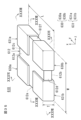
- FIG. 1 is an external perspective view showing a multilayer capacitor according to a first embodiment of the present invention
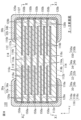
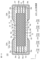
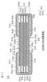
- 2 is a cross-sectional view taken along line II-II in FIG. 1.
- 3 is a cross-sectional view taken along line III-III in FIG. 1.
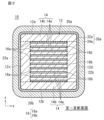
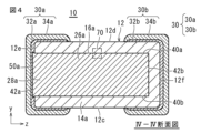
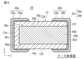
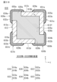
- FIG. 3 is a cross-sectional view taken along line IV-IV in FIG. 3 is a cross-sectional view taken along line VV in FIG. 2.
- 3A is an enlarged view of the ⁇ portion in Fig. 2
- Fig. 3B is an enlarged view of the ⁇ portion in Fig. 2.
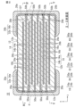
- FIG. 5 is a diagram showing measurement points in FIG. 4 .
- 2 is a cross-sectional view of a multilayer capacitor according to a second embodiment of the present invention, taken along line II-II in FIG. 1.
- FIG. 3 is a cross-sectional view of the multilayer capacitor according to the second embodiment of the present invention, taken along line III-III in FIG. 1.
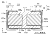
- 9 is a cross-sectional view taken along line XX in FIG. 8 .
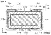
- 10 is a cross-sectional view taken along line XI-XI in FIG. 8.
- FIG. 13 is an external perspective view showing a multilayer capacitor in accordance with a third embodiment of the present invention.
- FIG. 13 is a front view showing a multilayer capacitor according to a third embodiment of the present invention.
- FIG. 11 is a top view showing a multilayer capacitor according to a third embodiment of the present invention.
- 13 is a cross-sectional view taken along line XV-XV in FIG. 12.
- FIG. 13 is a cross-sectional view taken along line XVI-XVI in FIG. 12.
- FIG. 13 is an exploded perspective view of the laminate shown in FIG. 12 .
- FIG. 13 is an external perspective view showing a multilayer capacitor in accordance with a fourth embodiment of the present invention.
- FIG. 13 is a front view showing a multilayer capacitor according to a fourth embodiment of the present invention.
- FIG. 13 is a top view showing a multilayer capacitor according to a fourth embodiment of the present invention.
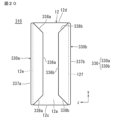
- 19 is a cross-sectional view taken along line XXI-XXI in FIG. 18.
- 19 is a cross-sectional view taken along line XXII-XXII in FIG. 18.
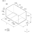
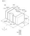
- FIG. 13 is an external perspective view showing a multilayer capacitor in accordance with a fifth embodiment of the present invention.
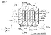
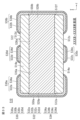
- 24 is a cross-sectional view taken along line XXIV-XXIV in FIG. 23.
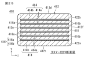
- 24 is a cross-sectional view taken along line XXV-XXV in FIG. 23.
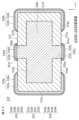
- 25 is a cross-sectional view taken along line XXVI-XXVI in FIG. 24.
- FIG. 24 is an exploded perspective view of the laminate shown in FIG. 23.
- FIG. 13 is an external perspective view showing a multilayer capacitor in accordance with a sixth embodiment of the present invention.
- FIG. 13 is a top view showing a multilayer capacitor in accordance with a sixth embodiment of the present invention.
- FIG. 13 is a front view showing a multilayer capacitor in accordance with a sixth embodiment of the present invention.
- 29 is a cross-sectional view taken along line XXXI-XXXI in FIG. 28.
- 29 is a cross-sectional view taken along line XXXII-XXXII in FIG. 28.
- 32 is a cross-sectional view taken along line XXXIII-XXXIII in FIG. 31 .
- 32 is a cross-sectional view taken along line XXIV-XXXIV in FIG. 31 .
- FIG. 13 is an external perspective view showing a multilayer capacitor in accordance with a seventh embodiment of the present invention.
- FIG. 36 is a cross-sectional view taken along line XXXVI-XXXVI in FIG.
- FIG. 36 is a cross-sectional view taken along line XXXVII-XXXVII in FIG. 35 .
- FIG. 36 is a cross-sectional view taken along line XXXVIII-XXXVIII in FIG. 35 .
- FIG. 36 is an exploded perspective view of the laminate shown in FIG. 35 .
- FIG. 13 is an external perspective view showing a multilayer capacitor in accordance with an eighth embodiment of the present invention. This is a cross-sectional view taken along line XXXI-XXXXI in Figure 40.
- This is a cross-sectional view taken along line XXXII-XXXXII in Figure 40.
- FIG. 41 is an exploded perspective view of the laminate shown in FIG. 40.
- FIG. 1 is an external perspective view showing a multilayer capacitor according to a first embodiment of the present invention.
- FIG. 2 is a cross-sectional view taken along line II-II in FIG. 1.
- FIG. 3 is a cross-sectional view taken along line III-III in FIG. 1.
- FIG. 4 is a cross-sectional view taken along line IV-IV in FIG. 2.
- FIG. 5 is a cross-sectional view taken along line V-V in FIG. 2.
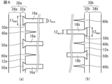
- FIG. 6(a) is an enlarged view of an ⁇ portion in FIG. 2.
- FIG. 6(b) is an enlarged view of a ⁇ portion in FIG. 2.
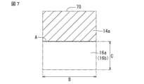
- FIG. 7 is a diagram showing measurement points in FIG. 4.
- the multilayer capacitor 10 has a laminate 12 and an external electrode 30. Below, the configuration of each will be explained in the order of the laminate 12 and the external electrode 30.
- the laminate 12 includes a first main surface 12a and a second main surface 12b facing the stacking direction x, a first side surface 12c and a second side surface 12d facing the width direction y perpendicular to the stacking direction x, and a first end surface 12e and a second end surface 12f facing the length direction z perpendicular to the stacking direction x and the width direction y.
- the first main surface 12a and the second main surface 12b extend along the width direction y and the length direction z, respectively.
- the first side surface 12c and the second side surface 12d extend along the stacking direction x and the length direction z, respectively.
- the first end surface 12e and the second end surface 12f extend along the stacking direction x and the width direction y, respectively.
- the stacking direction x is the direction connecting the first main surface 12a and the second main surface 12b
- the width direction y is the direction connecting the first side surface 12c and the second side surface 12d
- the length direction z is the direction connecting the first end surface 12e and the second end surface 12f.
- the surfaces of the first main surface 12a and the second main surface 12b, the first side surface 12c and the second side surface 12d, and the first end surface 12e and the second end surface 12f may be provided with irregularities, or may be roughened.
- the corners and ridges of the laminate 12 are rounded. Note that a corner refers to a portion where three adjacent faces of the laminate 12 intersect, and a ridge refers to a portion where two adjacent faces of the laminate 12 intersect.
- the laminate 12 includes a plurality of laminated resin layers 14 and a plurality of internal electrode layers 16.
- the resin layers 14 include an inner resin layer 14a and an outer resin layer 14b.
- the internal electrode layers 16 include a first internal electrode layer 16a and a second internal electrode layer 16b.
- the laminate 12 comprises an inner layer 18 and two outer layer sections 20a, 20b arranged to sandwich the inner layer section 18 in the stacking direction x.
- the outer layer section on the first main surface 12a side is referred to as the first main surface side outer layer section 20a
- the outer layer section on the second main surface 12b side is referred to as the second main surface side outer layer section 20b.
- the laminate 12 also comprises two outer layer sections 22a, 22b arranged to sandwich the inner layer section 18 in the width direction y.
- the outer layer section on the first side surface 12c side is referred to as the first side surface side outer layer section 22a
- the outer layer section on the second side surface 12d side is referred to as the second side surface side outer layer section 22b.
- the laminate 12 has an inner layer portion 18 composed of one or more inner resin layers 14a and multiple internal electrode layers 16 arranged thereon.
- the internal electrode layers 16 have a first internal electrode layer 16a that is extended to the first end face 12e and a second internal electrode layer 16b that is extended to the second end face 12f.
- the multiple first internal electrode layers 16a and second internal electrode layers 16b face each other via the inner resin layer 14a.
- the laminate 12 has a first main surface side outer layer portion 20a located on the first main surface 12a side and formed from a plurality of outer layer resin layers 14b located between the first main surface 12a and the outermost surface of the inner layer portion 18 on the first main surface 12a side and a straight line adjacent to that outermost surface.
- the laminate 12 has a second main surface side outer layer portion 20b located on the second main surface 12b side and formed from a plurality of outer layer resin layers 14b located between the second main surface 12b and the outermost surface of the inner layer portion 18 on the second main surface 12b side and a straight line adjacent to that outermost surface.
- the laminate 12 has a first side outer layer portion 22a located on the first side surface 12c side and formed from a plurality of outer resin layers 14b located between the first side surface 12c and the outermost surface of the inner layer portion 18 on the first side surface 12c side.
- the laminate 12 has a second side surface outer layer portion 22b located on the second side surface 12d side and formed from a plurality of outer layer resin layers 14b located between the second side surface 12d and the outermost surface of the inner layer portion 18 on the second side surface 12d side.
- the resin layer 14, i.e., the inner resin layer 14a and the outer resin layer 14b, may be made of, but is not limited to, a liquid crystal polymer (LCP) resin, which has excellent heat resistance, an epoxy resin, or a polyimide resin.
- LCP liquid crystal polymer
- the outer resin layers 14b of the first main surface side outer layer 20a, the second main surface side outer layer 20b, the first side surface side outer layer 22a, and the second side surface side outer layer 22b are each formed from the same type of resin material as the inner resin layer 14a.
- the first main surface side outer layer 20a, the second main surface side outer layer 20b, the first side surface side outer layer 22a, and the second side surface side outer layer 22b may each be composed of multiple outer resin layers 14b or a single outer resin layer 14b.
- the inner resin layer 14a and the outer resin layer 14b can be formed using different components. For example, it is possible to change the inner resin layer 14a to one with a high dielectric constant and the outer resin layer 14b to one with good moisture resistance, weather resistance, and strength resistance.
- the number of inner resin layers 14a and outer resin layers 14b to be laminated is not particularly limited, but it is preferable that the number be 15 or more and 200 or less, including the outer resin layers 14b. In addition, it is preferable that the thickness of the inner resin layer 14a be 0.2 ⁇ m or more and 10.0 ⁇ m or less.
- the internal electrode layer 16 includes a first internal electrode layer 16a and a second internal electrode layer 16b.
- the first internal electrode layer 16a and the second internal electrode layer 16b are alternately stacked with the inner resin layer 14a interposed therebetween. Note that, below, the internal electrode layer may be referred to as the internal electrode.
- the first internal electrode layer 16a is disposed between two of the multiple inner resin layers 14a, and is exposed to at least one of the first main surface 12a, the second main surface 12b, the first side surface 12c, the second side surface 12d, the first end surface 12e, and the second end surface 12f.
- the first internal electrode layer 16a is disposed between two of the inner resin layers 14a, and is exposed to the first end surface 12e.
- the second internal electrode layer 16b is disposed between two of the multiple inner resin layers 14a, and is exposed to at least one of the first main surface 12a, the second main surface 12b, the first side surface 12c, the second side surface 12d, the first end surface 12e, and the second end surface 12f.
- the second internal electrode layer 16b is disposed between two of the inner resin layers 14a, and is exposed to the second end surface 12f.
- the first internal electrode layer 16a is disposed on the surface of the inner resin layer 14a.
- the first internal electrode layer 16a has a first opposing electrode portion 26a that faces the second internal electrode layer 16b, and a first extraction electrode portion 28a that is located on one end side of the first internal electrode layer 16a and extends from the first opposing electrode portion 26a to the first end face 12e of the laminate 12. The end of the first extraction electrode portion 28a is extended to the first end face 12e and exposed.
- the shape of the first opposing electrode portion 26a of the first internal electrode layer 16a is not particularly limited, but is preferably rectangular in plan view. However, the corners in plan view may be rounded or may be formed at an angle in plan view (tapered). It may also be tapered in plan view, with a slope in either direction.
- the shape of the first extraction electrode portion 28a of the first internal electrode layer 16a is not particularly limited, but is preferably rectangular in plan view. However, the corners in plan view may be rounded or may be formed at an angle in plan view (tapered). It may also be tapered in plan view, with a slope in either direction.
- the length in the width direction y of the first opposing electrode portion 26a of the first internal electrode layer 16a and the length in the width direction y of the first extraction electrode portion 28a of the first internal electrode layer 16a may be different, or the length in the width direction y may change toward the first end face 12e side where the first internal electrode layer 16a is exposed.
- the second internal electrode layer 16b is disposed on a surface of an inner resin layer 14a different from the inner resin layer 14a on which the first internal electrode layer 16a is disposed.
- the second internal electrode layer 16b has a second opposing electrode portion 26b that faces the first internal electrode layer 16a, and a second extraction electrode portion 28b that is located on one end side of the second internal electrode layer 16b and extends from the second opposing electrode portion 26b to the second end face 12f of the laminate 12. The end of the second extraction electrode portion 28b is extended to the second end face 12f and exposed.
- the shape of the second opposing electrode portion 26b of the second internal electrode layer 16b is not particularly limited, but is preferably rectangular in plan view. However, the corners in plan view may be rounded or may be formed at an angle in plan view (tapered). It may also be tapered in plan view, with a slope in either direction.
- the shape of the second extraction electrode portion 28b of the second internal electrode layer 16b is not particularly limited, but is preferably rectangular in plan view. However, the corners in plan view may be rounded or may be formed at an angle in plan view (tapered). It may also be tapered in plan view, with a slope in either direction.
- the length in the width direction y of the second opposing electrode portion 26b of the second internal electrode layer 16b and the length in the width direction y of the second extraction electrode portion 28b of the second internal electrode layer 16b may be different, or the length in the width direction y may change toward the second end face 12f side where the second internal electrode layer 16b is exposed.
- the first internal electrode layer 16a and the second internal electrode layer 16b face each other via the inner resin layer 14a, generating capacitance.
- the first internal electrode layer 16a and the second internal electrode layer 16b can be made of an appropriate conductive material, for example, metals such as Ni, Cu, Ag, Pd, Au, or an Ag-Pd alloy that contains one of these metals, but are not limited to these.
- the first internal electrode layer 16a and the second internal electrode layer 16b are made mainly of Cu, which has good conductivity. This can reduce the ESR of the multilayer capacitor 10.
- the dielectric constant of the inner resin layer 14a is lower than that of the dielectric material used in conventional laminated capacitors, the area of the opposing electrode portions 26a, 26b must be increased accordingly to form a capacitor with the same capacitance.
- This requires increasing the number of laminated layers of the first inner electrode layer 16a and the second inner electrode layer 16b.
- the total area of the internal electrode layers 16 increases, and the ESR of the laminated capacitor 10 can be reduced.
- the laminate 12 has the inner resin layer 14a and the outer resin layer 14b, even if the laminated capacitor 10 is deflected, it can be cushioned by the inner resin layer 14a and the outer resin layer 14b, and the deflection strength can be improved. Therefore, the mechanical strength can be improved compared to conventional laminated capacitors.
- the sintering temperature of the dielectric ceramic is higher than that of the internal electrode 16 when the dielectric ceramic is fired, so that over-sintering of the internal electrode 16 may cause the particles to bond together, resulting in voids in the internal electrode 16, which may reduce the effective area and the linearity of the ends of the internal electrode 16.
- the multilayer capacitor 10 can be formed without including a firing process at a temperature exceeding the melting point of the inner resin layer 14a, there is no reduction in the effective area or linearity due to over-sintering of the first internal electrode layer 16a and the second internal electrode layer 16b. Therefore, the area of the internal electrode 16 per unit number can be maximized, and the capacity can be maximized. Furthermore, the linearity of the ends of the internal electrode 16 can be improved, which reduces the ESR.
- the first internal electrode layer 16a and the second internal electrode layer 16b have no voids. This shortens the current path of the multilayer capacitor 10, thereby reducing the ESR.
- the first internal electrode layer 16a has an end 40a in the width direction y on the first side surface 12c side, an end 40b in the width direction y on the second side surface 12d side, an end 42a in the length direction z on the first end surface 12e side, and an end 42b in the length direction z on the second end surface 12f side.
- the end 42a on the first end surface 12e side of the first internal electrode layer 16a is exposed from the laminate 12.
- the end 40a on the first side surface 12c side, the end 40b on the second side surface 12d side, and the end 42b on the second end surface 12f side of the first internal electrode layer 16a are in contact with the inner resin layer 14a.
- the second internal electrode layer 16b has an end 40c in the width direction y on the first side surface 12c side, an end 40d in the width direction y on the second side surface 12d side, an end 42c in the length direction z on the first end surface 12e side, and an end 42d in the length direction z on the second end surface 12f side.
- the end 42d on the second end surface 12f side of the second internal electrode layer 16b is exposed from the laminate 12.
- the end 40c on the first side surface 12c side, the end 40d on the second side surface 12d side, and the end 42c on the first end surface 12e side of the second internal electrode layer 16b are in contact with the inner resin layer 14a.
- the linearity of the end of the first internal electrode layer 16a or the second internal electrode layer 16b where the first internal electrode layer 16a or the second internal electrode layer 16b contacts the inner resin layer 14a is preferably 1.0 or more and 1.5 or less. Furthermore, the linearity of the end of the first internal electrode layer 16a or the second internal electrode layer 16b where the first internal electrode layer 16a or the second internal electrode layer 16b contacts the inner resin layer 14a is preferably 1.0. This allows the current path to be formed as close to the shortest path as possible, thereby reducing the ESR.
- the linearity of the ends 40a, 40b of the first internal electrode layer 16a in the width direction y is calculated by the following method. First, the substrate is polished in the length direction z and width direction y (LW cross section) to expose the first internal electrode layer 16a. Next, a scanning electron microscope (SEM) is used to take an SEM image of the ends 40a, 40b of the first internal electrode layer 16a exposed on the surface in the width direction y at a magnification of 2000 times, centered on 1/2L of the multilayer capacitor 10, and the perimeter, average vertical chord length, and image width are measured.
- Figure 7 is a diagram showing a measurement point 70 in Figure 4.
- the length of the end of the internal electrode layer is A
- the image width is B
- the average vertical chord length is C
- the perimeter is D.
- the perimeter, average vertical chord length, and image width are measured, and the lengths ⁇ A> of the ends 40a, 40b of the first internal electrode layer 16a are calculated by (Equation 1).
- (Equation 1) (End length ⁇ A>) (Circumference length ⁇ D>) - (Average vertical chord length ⁇ C>) x 2 - (Image width ⁇ B>)
- the linearity of the ends 40a, 40b of the first internal electrode layer 16a is calculated using (Equation 2).
- (Equation 2) (Edge Linearity) (Edge Length ⁇ A>)/(Image Width ⁇ B>)
- the linearity of the end portion 42b of the first internal electrode layer 16a in the length direction z is calculated by the following method.
- the substrate is polished in the length direction z and width direction y (LW cross section) to expose the first internal electrode layer 16a.
- a scanning electron microscope (SEM) is used to take an SEM image of the end 42b in the length direction z of the first internal electrode layer 16a exposed on the surface at a magnification of 2000 times, centered on 1/2 W of the multilayer capacitor 10, and the perimeter, average vertical chord length, and image width are measured.
- the length of the end of the internal electrode layer is designated as A, the image width as B, the average vertical chord length as C, and the perimeter as D. From the SEM image, the perimeter, average vertical chord length, and image width are measured, and the linearity of the end 42b in the length direction z of the first internal electrode layer 16a is calculated using the above (Equation 1) and (Equation 2).
- the linearity of the ends 40c, 40d of the second internal electrode layer 16b in the width direction y is calculated by the following method. First, the second internal electrode layer 16b is exposed by polishing in the length direction z and the width direction y (LW cross section). Next, a scanning electron microscope (SEM) is used to take an SEM image of the ends 40c, 40d of the second internal electrode layer 16b in the width direction y exposed on the surface at a magnification of 2000 times centered on 1/2L of the multilayer capacitor 10, and the perimeter, average vertical chord length, and image width are measured.
- the length of the end of the internal electrode layer is A
- the image width is B
- the average vertical chord length is C
- the perimeter is D.
- the perimeter, average vertical chord length, and image width are measured from the SEM image, and the linearity of the ends 40c, 40d of the second internal electrode layer 16b in the width direction y is calculated using the above (Equation 1) and (Equation 2).
- the linearity of the end portion 42c of the second internal electrode layer 16b in the longitudinal direction z is calculated by the following method.
- the second internal electrode layer 16b is exposed by polishing in the length direction z and the width direction y (LW cross section).
- a scanning electron microscope (SEM) is used to take an SEM image of the end 42c in the length direction z of the second internal electrode layer 16b exposed on the surface at a magnification of 2000 times, centered on 1/2W of the multilayer capacitor 10, and the perimeter, average vertical chord length, and image width are measured.
- the length of the end of the internal electrode layer is designated as A, the image width as B, the average vertical chord length as C, and the perimeter as D. From the SEM image, the perimeter, average vertical chord length, and image width are measured, and the linearity of the end 42c in the length direction z of the second internal electrode layer 16b is calculated using the above (Equation 1) and (Equation 2).
- the end 42a on the first end face 12e side which is the end exposed on any one of the first side face 12c, the second side face 12d, the first end face 12e, and the second end face 12f of the laminate 12, of the first internal electrode layer 16a, is thinner in thickness in the stacking direction x toward the face (second end face 12f) opposite to the exposed face of the first internal electrode layer 16a.
- the first internal electrode layer 16a when the first internal electrode layer 16a is exposed on the first end face 12e, the first internal electrode layer 16a is formed in a substantially triangular shape with a shorter length in the stacking direction x from the first end face 12e toward the second end face 12f side in the cross section (LT cross section) in the stacking direction x and the length direction z. This increases the bonding area between the first external electrode 30a and the first internal electrode layer 16a, increasing the adhesion strength and reducing the ESR.
- the end 42a on the first end face 12e side which is the end exposed to any one of the first side face 12c, second side face 12d, first end face 12e and second end face 12f of the laminate 12, among the ends 40a, 40b, 42a, 42b of the first internal electrode layer 16a, is defined as a region where the thickness in the stacking direction x decreases toward the face (second end face 12f) opposite the exposed face of the first internal electrode layer 16a, then it is preferable that the entire first exposed end region 50a is exposed from the laminate 12.
- the end 42a exposed at the first end face 12e of the laminate 12 has a first exposed end region 50a, which is a region in which the thickness in the lamination direction x is reduced toward the second end face 12f opposite the exposed first end face 12e of the first internal electrode layer 16a, and it is preferable that the entire first exposed end region 50a is exposed from the first end face 12e.
- the thickness of the first internal electrode layer 16a in the stacking direction x is defined as the thickest part t1max and the thinnest part t1min .
- the ratio of the thickness of the first internal electrode layer 16a in the stacking direction x between the thickest part t1max and the thinnest part t1min is preferably such that the thickest part t1max is 1.5 times or more and 2.5 times or less than the thinnest part t1min .
- the first exposed end region 50a can be formed, for example, by immersing the first end surface 12e of the laminate 12 in an etching solution and etching the inner resin layer 14a.
- the end 42d on the second end face 12f side which is the end exposed to any one of the first side face 12c, the second side face 12d, the first end face 12e, and the second end face 12f of the laminate 12, has a thickness in the stacking direction x that is thinner toward the face (first end face 12e) opposite to the exposed face of the second internal electrode layer 16b.
- the second internal electrode layer 16b when the second internal electrode layer 16b is exposed to the second end face 12f, the second internal electrode layer 16b is formed to have a substantially triangular shape with a shorter length in the stacking direction x from the second end face 12f toward the first end face 12e side in the cross section (LT cross section) in the stacking direction x and the length direction z.
- This increases the bonding area between the second external electrode 30b and the second internal electrode layer 16b, increasing the adhesion strength and reducing the ESR.
- the second exposed end region 50b which is the region where the thickness in the stacking direction x decreases toward the surface (first end face 12e) opposite the exposed surface of the second internal electrode layer 16b, it is preferable that the entire second exposed end region 50b is exposed from the laminate 12.
- the end 42d exposed at the second end face 12f of the laminate 12 has a second exposed end region 50b, which is a region in which the thickness in the lamination direction x is thinner toward the first end face 12e opposite the exposed second end face 12f of the second internal electrode layer 16b, and it is preferable that the entire second exposed end region 50b is exposed from the second end face 12f.
- the thickness of the second internal electrode layer 16b in the stacking direction x is defined as the thickest part t2max and the thinnest part t2min .
- the ratio of the thickness of the second internal electrode layer 16b in the stacking direction x between the thickest part t2max and the thinnest part t2min is preferably such that the thickest part t2max is 1.5 times or more and 2.5 times or less than the thinnest part t2min .
- the second exposed end region 50b can be formed, for example, by immersing the second end surface 12f of the laminate 12 in an etching solution and etching the inner resin layer 14a.
- the thickness of the stacking direction x of the ends 40a, 40b in the width direction y of the first internal electrode layer 16a thicker than the thickness of the stacking direction x of the center of the width direction y of the first internal electrode layer 16a.
- the total number of the first internal electrode layers 16a and the second internal electrode layers 16b is preferably 15 or more and 200 or less.
- the thickness of the first internal electrode layers 16a and the second internal electrode layers 16b is preferably 1 ⁇ m or more and 12 ⁇ m or less.
- the laminate 12 may have a first cut portion 60a from the first end face 12e where the first internal electrode layer 16a is exposed toward the second end face 12f, which is the opposite face.
- the laminate 12 may have a second cut portion 60b from the second end face 12f where the second internal electrode layer 16b is exposed toward the first end face 12e, which is the opposite face. This allows the external electrode 30 to penetrate into the first cut portion 60a and the second cut portion 60b, and the anchor effect can improve the adhesive strength between the laminate 12 and the external electrode 30.
- the first cut portion 60a and the second cut portion 60b can be formed, for example, by immersing the first end surface 12e and the second end surface 12f of the laminate 12 in an etching solution and etching the inner resin layer 14a.
- the external electrode 30 has a first external electrode 30a and a second external electrode 30b.
- the first external electrode 30a is disposed on one or more of the first main surface 12a, the second main surface 12b, the first side surface 12c, the second side surface 12d, the first end surface 12e, and the second end surface 12f of the laminate 12.
- the first external electrode 30a is connected to the first internal electrode layer 16a, and is disposed so as to extend from the first end surface 12e around the first main surface 12a, the second main surface 12b, the first side surface 12c, and a portion of the second side surface 12d.
- the electrode may be disposed, for example, so as not to extend from the first end surface 12e around the first side surface 12c and the second side surface 12d.
- the second external electrode 30b is disposed on one or more of the first main surface 12a, the second main surface 12b, the first side surface 12c, the second side surface 12d, the first end surface 12e, and the second end surface 12f of the laminate 12.
- the second external electrode 30b is connected to the second internal electrode layer 16b, and is disposed so as to extend from the second end surface 12f around the first main surface 12a, the second main surface 12b, the first side surface 12c, and a part of the second side surface 12d.
- the electrode 30b may be disposed, for example, so as not to extend from the second end surface 12f around the first side surface 12c and the second side surface 12d.
- the external electrode 30 is composed of an underlying electrode layer 32 arranged on at least one of the first principal surface 12a, the second principal surface 12b, the first side surface 12c, the second side surface 12d, the first end surface 12e, and the second end surface 12f, and a plating layer 34 that covers the underlying electrode layer 32.
- the base electrode layer 32 has a first base electrode layer 32a and a second base electrode layer 32b.
- the first base electrode layer 32a is disposed so as to wrap around from the first end face 12e to the first main surface 12a, the second main surface 12b, the first side surface 12c, and a portion of the second side surface 12d.
- the second base electrode layer 32b is disposed so as to wrap around from the second end face 12f to the first main surface 12a, the second main surface 12b, the first side surface 12c, and a portion of the second side surface 12d.
- the base electrode layer 32 includes at least one selected from a baked layer, a conductive resin layer, a thin film layer, etc.
- the baked layer contains a metal component and a glass component.
- the glass component contains at least one selected from B, Si, Ba, Mg, Al, Li, Zn, Ti, etc.
- the metal component of the baked layer contains at least one selected from Cu, Ni, Ag, Pd, Ag-Pd alloy, Au, etc. It is preferable that the metal component of the baked layer is made of a metal such as Cu or Ni. In the case of a baked layer, the metal component acts as a conductive component. Furthermore, the baked layer may be a multi-layered layer.
- the baked layer is formed by applying a conductive paste containing a glass component and a metal component to the laminate 12 and baking it.
- the baked layer may be formed by simultaneously baking a laminated chip having an internal electrode layer 16 and an inner resin layer 14a and a conductive paste applied to the laminated chip, or may be formed by baking a laminated chip having an internal electrode layer 16 and an inner resin layer 14a to obtain the laminate 12, and then applying and baking a conductive paste.
- the baking temperature is preferably lower than the melting point of the inner resin layer 14a. More specifically, the baking temperature is preferably 200°C or lower.
- the thickness in the length direction z connecting the first end face 12e and the second end face 12f of the first baked layer and the second baked layer at the center of the stacking direction x connecting the first main surface 12a and the second main surface 12b of the first baked layer and the second baked layer located at the first end face 12e and the second end face 12f is preferably, for example, 5 ⁇ m or more and 60 ⁇ m or less.
- the thickness in the stacking direction x connecting the first main face 12a and the second main face 12b of the first baked layer and the second baked layer is preferably, for example, 0.5 ⁇ m or more and 20 ⁇ m or less.
- the conductive resin layer includes a thermosetting resin and a metal. Since the conductive resin layer includes a thermosetting resin, it is more flexible than a baked layer made of, for example, a plating film or a baked product of a conductive paste. Therefore, even if the multilayer capacitor 10 is subjected to a physical impact or an impact due to a thermal cycle, the conductive resin layer functions as a buffer layer, and it is possible to further prevent cracks in the multilayer capacitor 10.
- the metal contained in the conductive resin layer can be Ag, Cu, Ni, Sn, Bi, or an alloy containing these. It is also possible to use a metal powder with an Ag coating on the surface. When using a metal powder with an Ag coating on the surface, it is preferable to use Cu, Ni, Sn, Bi, or an alloy powder of these.
- the reason for using Ag conductive metal powder as the conductive metal is that Ag has the lowest resistivity of all metals, making it suitable as an electrode material, and Ag is a precious metal, so it does not oxidize and has high weather resistance. In addition, it is possible to use a cheaper base metal while maintaining the above-mentioned properties of Ag. In the case of a conductive resin layer, the conductive metal acts as the conductive component.
- the metal contained in the conductive resin layer may be Cu or Ni that has been subjected to an anti-oxidation treatment.
- the metal contained in the conductive resin layer may be a metal powder whose surface is coated with Sn, Ni, or Cu.
- Ag, Cu, Ni, Sn, Bi, or an alloy powder of these metals it is preferable to use Ag, Cu, Ni, Sn, Bi, or an alloy powder of these metals.
- the metal contained in the conductive resin layer is mainly responsible for the electrical conductivity of the conductive resin layer. Specifically, when the conductive fillers come into contact with each other, an electrical path is formed inside the conductive resin layer.
- the metal contained in the conductive resin layer can be spherical or flat, but it is preferable to use a mixture of spherical metal powder and flat metal powder.
- thermosetting resins such as epoxy resin, phenolic resin, urethane resin, silicone resin, polyimide resin, etc.
- epoxy resin which has excellent heat resistance, moisture resistance, adhesion, etc., is one of the most suitable resins.
- the conductive resin layer preferably contains a curing agent in addition to the thermosetting resin.
- a curing agent in addition to the thermosetting resin.
- various known compounds such as phenol-based, amine-based, acid anhydride-based, imidazole-based, active ester-based, and amide-imide-based compounds can be used as the curing agent for the epoxy resin.
- the thickest part of the conductive resin layer is preferably, for example, 5 ⁇ m or more and 60 ⁇ m or less.
- the base electrode layer 32 is formed from a thin film layer.
- the thin film layer is formed by a thin film formation method such as a sputtering method or a vapor deposition method.
- the thin film layer is a layer of 1 ⁇ m or less in which metal particles are deposited.
- the base electrode layer 32 may be directly formed by a plating layer.
- the multilayer capacitor 10 may have a structure including a plating layer that is directly electrically connected to the internal electrode layer 16.
- a catalyst may be disposed on the surface of the laminate 12 as a pretreatment, and then the plating layer may be directly formed.
- the plating layer formed as the base electrode layer 32 contains at least one metal selected from, for example, Cu, Ni, Sn, Pb, Au, Ag, Pd, Bi, or Zn, or an alloy containing such a metal.
- the plating layer formed as the base electrode layer 32 does not contain glass. Furthermore, it is preferable that the metal ratio per unit volume of the plating layer formed as the base electrode layer 32 is 99 volume % or more.
- the height can be reduced, i.e., the thickness can be converted to the thickness of the laminate 12, i.e., the thickness of the inner layer 18, thereby improving the design freedom of thin chips.
- the base electrode layer 32 may be formed from one of the above four configurations, or the base electrode layer 32 may be formed from a combination of the above four configurations.
- the plating layer 34 has a first plating layer 34a and a second plating layer 34b.
- the first plating layer 34a is disposed so as to cover the first base electrode layer 32a.
- the second plating layer 34b is disposed so as to cover the second base electrode layer 32b.
- the plating layer 34 includes, for example, at least one selected from Cu, Ni, Sn, Ag, Pd, Ag-Pd alloy, Au, etc.
- the plating layer 34 preferably has at least a two-layer structure.
- Ni plating and Sn plating are arranged in this order from the laminate 12 side.
- Sn plating, Ni plating, and Sn plating are arranged in this order from the laminate 12 side.
- the Ni plating can prevent the base electrode layer 32 from being eroded by solder when mounting the multilayer capacitor 10.
- the Sn plating can improve the wettability of the solder when mounting the multilayer capacitor 10, thereby improving mountability.
- each plating layer 34 is 1 ⁇ m or more and 6 ⁇ m or less.
- the dimension in the length direction z of the multilayer capacitor 10, including the laminate 12, the first external electrode 30a, and the second external electrode 30b, is defined as dimension L
- the dimension in the width direction y of the multilayer capacitor 10, including the laminate 12, the first external electrode 30a, and the second external electrode 30b is defined as dimension W
- the dimension in the stacking direction x of the multilayer capacitor 10, including the laminate 12, the first external electrode 30a, and the second external electrode 30b is defined as dimension T.
- the dimensions of the multilayer capacitor 10 are not limited, but it is preferable that, for example, the L dimension in the length direction z is 0.20 mm or more and 0.65 mm or less, the W dimension in the width direction y is 0.10 mm or more and 0.35 mm or less, and the T dimension in the stacking direction x is 0.01 mm or more and 0.35 mm or less.
- the inner layer 18 of the laminate 12 is formed by alternately stacking a plurality of inner resin layers 14a and a plurality of internal electrode layers 16.
- the baking process can be performed at a temperature lower than usual, and the metal components of the internal electrode layers 16 can be prevented from being over-sintered.
- the generation of voids in the internal electrode layers 16 can be suppressed, and the shape of the ends of the internal electrode layers 16 can be prevented from becoming irregular.
- the ends of the internal electrode layers 16 become regular, i.e., the ends of the internal electrode layers 16 become linear, which shortens the current path and reduces the ESR.
- the inner resin layer 14a and the outer resin layer 14b are resin sheets whose main material is a thermoplastic resin such as liquid crystal polymer (LCP).
- LCP liquid crystal polymer
- a conductor pattern that will become the internal electrode layer 16 is formed on the resin sheets that will become the multiple inner resin layers 14a. More specifically, a metal foil such as Cu foil is laminated on one side of the resin sheets that will become the inner resin layers 14a, and the metal foil is patterned by photolithography and stacked. At this time, for example, the surface of one side of the resin sheet that will become the inner resin layer 14a may be roughened, and Cu foil may be laminated on top of it to improve the adhesive strength between the inner resin layer 14a and the internal electrode layer 16. This forms a block for the inner layer portion. In addition, resin sheets that will become the outer resin layers 14b are stacked to form multiple or single blocks for the first main surface side outer layer portion and multiple or single blocks for the second main surface side outer layer portion.
- the inner layer block is sandwiched between the first main surface side outer layer block and the second main surface side outer layer block, and then heated and pressed (collectively pressed) to produce a laminate block.
- the produced laminate block is cut into individual pieces, for example, by a dicer cut, to form the laminate 12.
- the first end face 12e and the second end face 12f of the laminate 12 may be immersed in an etching solution.
- the inner resin layer 14a is etched, the ends 42a, 42d of the internal electrode layer 16 are exposed, and the first exposed end region 50a and the second exposed end region 50b can be formed.
- a low-temperature curing conductive paste is applied to the first end face 12e and the second end face 12f of the obtained laminate 12, for example by a dipping method, and a baking process is performed at a temperature of 100°C to 250°C to form the base electrode layer 32.
- a dipping method for example by a dipping method
- a baking process is performed at a temperature of 100°C to 250°C to form the base electrode layer 32.
- the conductive paste can also be applied by a screen printing method.
- a conductive resin layer is formed as the base electrode layer 32
- a conductive resin paste containing a thermosetting resin and a metal component is applied to the first end face 12e and the second end face 12f of the obtained laminate 12, and heat treatment is performed at a temperature of 250° C. or less to harden the thermosetting resin to form the base electrode layer 32.
- the heat treatment atmosphere is preferably a N2 atmosphere, and the oxygen concentration is preferably suppressed to 100 ppm or less.
- the base electrode layer 32 can be formed by depositing metal particles on the first end face 12e and the second end face 12f of the obtained laminate 12, for example, by a sputtering method. This allows a thin film of 1.0 ⁇ m or less to be formed as the base electrode layer 32. At this time, by controlling the positional relationship with the laminate 12, such as the angle and distance, it is possible to control the thickness of the base electrode layer 32 and the amount of wrapping around the first main surface 12a, the second main surface 12b, the first side surface 12c, and the second side surface 12d of the laminate 12. In addition, the sputtering method may be applied to each surface individually, not just one surface.
- the first exposed end region 50a and the second exposed end region 50b may cause a step in the base electrode layer 32, and the base electrode layer 32 may be formed discontinuously in the lamination direction x.
- metal particles are deposited from one side, so that the first exposed end region 50a and the second exposed end region 50b may block the metal particles on the surface of each end face 12e, 12f of the laminate 12, resulting in a portion where the metal particles are not deposited, and the thin film layer may not be formed continuously.
- the internal electrode layer 16 and the external electrode 30 are electrically connected by the plating layer 34.
- electrolytic plating When forming a plating layer directly as the base electrode layer 32, electrolytic plating, electroless plating, etc. are used.
- electrolytic plating barrel plating is preferred.
- a plating layer 34 is formed on the formed base electrode layer 32 by, for example, barrel plating.
- the plating layer 34 has a two-layer structure, it is preferable that, for example, Ni plating and Sn plating are arranged in this order from the laminate 12 side.
- the metal types are not limited thereto.
- the plating layer 34 has a three-layer structure, it is preferable that, for example, Sn plating, Ni plating, and Sn plating are arranged in this order from the laminate 12 side.
- the multilayer capacitor 10 according to this embodiment is manufactured.
- Fig. 8 is a cross-sectional view of the multilayer capacitor according to the second embodiment of the present invention, taken along line II-II in Fig. 1.
- Fig. 9 is a cross-sectional view of the multilayer capacitor according to the second embodiment of the present invention, taken along line III-III in Fig. 1.
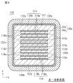
- Fig. 10 is a cross-sectional view taken along line XX in Fig. 8.
- Fig. 11 is a cross-sectional view taken along line XI-XI in Fig. 8.
- the multilayer capacitor 110 according to the second embodiment has a laminate 112 and an external electrode 30 having a configuration similar to that of the first embodiment.
- the laminate 112 is different from the laminate 12 according to the first embodiment in the structure of the internal electrode layer 116 of the laminate 112. Therefore, the same reference numerals are used for components corresponding to those of the multilayer capacitor 10 according to the first embodiment, and detailed description thereof will be omitted.
- the laminate 112 includes a first main surface 112a and a second main surface 112b facing the stacking direction x, a first side surface 112c and a second side surface 112d facing the width direction y perpendicular to the stacking direction x, and a first end surface 112e and a second end surface 112f facing the length direction z perpendicular to the stacking direction x and the width direction y.
- the first main surface 112a and the second main surface 112b extend along the width direction y and the length direction z, respectively.
- the first side surface 112c and the second side surface 112d extend along the stacking direction x and the length direction z, respectively.
- the first end surface 112e and the second end surface 112f extend along the stacking direction x and the width direction y, respectively. Therefore, the stacking direction x is the direction connecting the first main surface 112a and the second main surface 112b, the width direction y is the direction connecting the first side surface 112c and the second side surface 112d, and the length direction z is the direction connecting the first end surface 112e and the second end surface 112f.
- the surfaces of the first main surface 112a and the second main surface 112b, the first side surface 112c and the second side surface 112d, and the first end surface 112e and the second end surface 112f may be provided with irregularities, or may be roughened.
- the corners and ridges of the laminate 112 are rounded. Note that a corner refers to a portion where three adjacent faces of the laminate 112 intersect, and a ridge refers to a portion where two adjacent faces of the laminate 112 intersect. By rounding the corners and ridges of the laminate 112, chipping or cracking of the laminate 112 can be prevented.
- the laminate 112 includes a plurality of laminated resin layers 114 and a plurality of internal electrode layers 116.
- the resin layer 114 has an inner resin layer 114a and an outer resin layer 114b.
- the internal electrode layer 116 has a first internal electrode layer 116a, a second internal electrode layer 116b, and a floating internal electrode layer 116c.
- the laminate 112 includes an inner layer 118 and two outer layer sections 120a, 120b arranged to sandwich the inner layer section 118 in the stacking direction x.
- the outer layer section on the first main surface 112a side is referred to as the first main surface side outer layer section 120a
- the outer layer section on the second main surface 112b side is referred to as the second main surface side outer layer section 120b.
- the laminate 112 also includes two outer layer sections 122a, 122b arranged to sandwich the inner layer section 118 in the width direction y.
- the outer layer section on the first side surface 112c side is referred to as the first side surface side outer layer section 122a
- the outer layer section on the second side surface 112d side is referred to as the second side surface side outer layer section 122b.
- the laminate 112 has an inner layer section 118 composed of one or more inner resin layers 114a and multiple internal electrode layers 116 arranged thereon.
- the internal electrode layers 116 have a first internal electrode layer 116a that is extended to the first end face 112e and a second internal electrode layer 116b that is extended to the second end face 112f.
- the multiple first internal electrode layers 116a and second internal electrode layers 116b face each other via the inner resin layer 114a.
- the laminate 112 has a first main surface side outer layer portion 120a located on the first main surface 112a side and formed from a plurality of outer layer resin layers 114b located between the first main surface 112a and the outermost surface of the inner layer portion 118 on the first main surface 112a side and a straight line adjacent to that outermost surface.
- the laminate 112 has a second main surface side outer layer portion 120b located on the second main surface 112b side and formed from a plurality of outer layer resin layers 114b located between the second main surface 112b and the outermost surface of the inner layer portion 118 on the second main surface 112b side and a straight line adjacent to that outermost surface.
- the laminate 112 has a first side outer layer portion 122a located on the first side surface 112c side and formed from a plurality of outer resin layers 114b located between the first side surface 112c and the outermost surface of the inner layer portion 118 on the first side surface 112c side.
- the laminate 112 has a second side surface outer layer portion 122b located on the second side surface 112d side and formed from a plurality of outer layer resin layers 114b located between the second side surface 112d and the outermost surface of the inner layer portion 118 on the second side surface 112d side.
- the resin layer 114 i.e., the inner resin layer 114a and the outer resin layer 114b, may be made of, but is not limited to, a liquid crystal polymer (LCP) resin, which has excellent heat resistance, an epoxy resin, or a polyimide resin.
- LCP liquid crystal polymer
- the outer resin layers 114b of the first main surface side outer layer portion 120a, the second main surface side outer layer portion 120b, the first side surface side outer layer portion 122a, and the second side surface side outer layer portion 122b are formed from the same type of resin material as the inner resin layer 114a.
- the first main surface side outer layer portion 120a, the second main surface side outer layer portion 120b, the first side surface side outer layer portion 122a, and the second side surface side outer layer portion 122b may be composed of multiple outer resin layers 114b or may be composed of a single outer resin layer 114b.
- the inner resin layer 114a and the outer resin layer 114b are formed with different components. For example, it is possible to change the inner resin layer 114a to one with a high dielectric constant and the outer resin layer 114b to one with good moisture resistance, weather resistance, and strength resistance.
- the number of inner resin layers 114a and outer resin layers 114b to be stacked is not particularly limited, but it is preferable that the number be 15 or more and 200 or less, including the outer resin layers 114b. In addition, it is preferable that the thickness of the inner resin layer 114a be 0.2 ⁇ m or more and 10.0 ⁇ m or less.
- the internal electrode layer 116 includes a first internal electrode layer 116a, a second internal electrode layer 116b, and a floating internal electrode layer 116c.
- the first internal electrode layer 116a, the second internal electrode layer 116b, and the floating internal electrode layer 116c are alternately stacked with the inner resin layer 114a interposed therebetween.
- the first internal electrode layer 116a is disposed on the surface of the inner resin layer 114a.
- the first internal electrode layer 116a has a first opposing electrode portion 126a that faces the floating internal electrode layer 116c, and a first extraction electrode portion 128a that is located on one end side of the first internal electrode layer 116a and extends from the first opposing electrode portion 126a to the first end face 112e of the laminate 112. The end of the first extraction electrode portion 128a is drawn out to the first end face 112e and exposed.
- the shape of the first opposing electrode portion 126a of the first internal electrode layer 116a is not particularly limited, but is preferably rectangular in plan view. However, the corners in plan view may be rounded or may be formed at an angle in plan view (tapered). It may also be tapered in plan view, with a slope in either direction.
- the shape of the first extraction electrode portion 128a of the first internal electrode layer 116a is not particularly limited, but is preferably rectangular in plan view. However, the corners in plan view may be rounded or the corners may be formed at an angle in plan view (tapered). It may also be tapered in plan view, with a slope in either direction.
- the length in the width direction y of the first opposing electrode portion 126a of the first internal electrode layer 116a and the length in the width direction y of the first extraction electrode portion 128a of the first internal electrode layer 116a may be different, or the length in the width direction y may change toward the first end face 112e side where the first internal electrode layer 116a is exposed.
- the second internal electrode layer 116b is disposed on the surface of the same inner resin layer 114a as the inner resin layer 114a on which the first internal electrode layer 116a is disposed.
- the second internal electrode layer 116b has a second opposing electrode portion 126b that faces the floating internal electrode layer 116c, and a second extraction electrode portion 128b that is located on one end side of the second internal electrode layer 116b and extends from the second opposing electrode portion 126b to the second end surface 112f of the laminate 112. The end of the second extraction electrode portion 128b is extended to the second end surface 112f and exposed.
- the shape of the second opposing electrode portion 126b of the second internal electrode layer 116b is not particularly limited, but is preferably rectangular in plan view. However, the corners in plan view may be rounded or may be formed at an angle in plan view (tapered). It may also be tapered in plan view, with a slope in either direction.
- the shape of the second extraction electrode portion 128b of the second internal electrode layer 116b is not particularly limited, but is preferably rectangular in plan view. However, the corners in plan view may be rounded or may be formed at an angle in plan view (tapered). It may also be tapered in plan view, with a slope in either direction.
- the length in the width direction y of the second opposing electrode portion 126b of the second internal electrode layer 116b and the length in the width direction y of the second extraction electrode portion 128b of the second internal electrode layer 116b may be different, or the length in the width direction y may change toward the second end face 112f side where the second internal electrode layer 116b is exposed.
- the floating internal electrode layer 116c is disposed on a surface of the inner resin layer 114a different from the inner resin layer 114a on which the first internal electrode layer 116a and the second internal electrode layer 116b are disposed.
- the floating internal electrode layer 116c has a third opposing electrode portion 126c facing the first internal electrode layer 116a and a fourth opposing electrode portion 126d facing the second internal electrode layer 116b.
- the third opposing electrode portion 126c and the fourth opposing electrode portion 126d of the floating internal electrode layer 116c are formed so as to be continuous.
- the floating internal electrode layer 116c is not drawn out to either the first end surface 112e or the second end surface 112f. In FIG. 8 and FIG. 11, the third opposing electrode portion 126c and the fourth opposing electrode portion 126d of the floating internal electrode layer 116c are formed so as to be continuous, but may be divided.
- the shapes of the third opposing electrode portion 126c and the fourth opposing electrode portion 126d of the floating internal electrode layer 116c are not particularly limited, but are preferably rectangular in plan view. However, the corners in plan view may be rounded or may be formed at an angle in plan view (tapered). They may also be tapered in plan view, with a slope going in either direction.
- a floating internal electrode layer 116c is provided that is not drawn out to either the first end face 112e or the second end face 112f, and the floating internal electrode layer 116c divides the opposing electrode portion into two (two-unit structure).
- this is not limited to this, and for example, a three-unit structure, a four-unit structure, or a structure with more than four units may also be used.
- the first internal electrode layer 116a, the second internal electrode layer 116b, and the floating internal electrode layer 116c can be made of an appropriate conductive material, for example, metals such as Ni, Cu, Ag, Pd, Au, or an Ag-Pd alloy that contains one of these metals, but is not limited to this.
- the first internal electrode layer 116a, the second internal electrode layer 116b, and the floating internal electrode layer 116c are made mainly of Cu, which has good conductivity. This makes it possible to reduce the ESR of the multilayer capacitor 110.
- the dielectric constant of the inner resin layer 114a is lower than that of the dielectric material used in conventional laminated capacitors, the area of the opposing electrode parts 126a, 126b, 126c, and 126d must be increased accordingly to form a capacitor with the same capacitance. Therefore, it is necessary to increase the number of laminated layers of the first inner electrode layer 116a, the second inner electrode layer 116b, and the floating inner electrode layer 116c. As a result, the total area of the inner electrode layer 116 increases, and the ESR of the laminated capacitor 110 can be reduced.
- the laminate 112 since the laminate 112 has the inner resin layer 114a and the outer resin layer 114b, even if the laminated capacitor 110 is deflected, it can be cushioned by the inner resin layer 114a and the outer resin layer 114b, and the deflection strength can be improved. Therefore, the mechanical strength can be improved compared to conventional laminated capacitors.
- the sintering temperature of the dielectric ceramic is higher than that of the internal electrode 116 when the dielectric ceramic is fired, so that over-sintering of the internal electrode 116 may cause the particles to bond with each other, resulting in voids in the internal electrode 116, which may reduce the effective area and the linearity of the end of the internal electrode 116.
- the multilayer capacitor 110 can be formed without including a firing process at a temperature exceeding the melting point of the inner resin layer 114a, there is no reduction in the effective area or linearity due to over-sintering of the first internal electrode layer 116a, the second internal electrode layer 116b, and the floating internal electrode layer 116c. Therefore, the area of the internal electrode 116 per unit number can be maximized, and the maximum capacity can be obtained. Furthermore, the linearity of the end of the internal electrode 116 can be improved, which reduces the ESR.
- the first internal electrode layer 116a, the second internal electrode layer 116b, and the floating internal electrode layer 116c have no voids. This shortens the current path of the multilayer capacitor 110, thereby reducing the ESR.
- the linearity of the end of the first internal electrode layer 116a or the second internal electrode layer 116b where the first internal electrode layer 116a or the second internal electrode layer 116b contacts the inner resin layer 114a is preferably 1.0 or more and 1.5 or less. Furthermore, the linearity of the end of the first internal electrode layer 116a or the second internal electrode layer 116b where the first internal electrode layer 116a or the second internal electrode layer 116b contacts the inner resin layer 114a is preferably 1.0. This allows the current path to be formed as close to the shortest path as possible, thereby reducing the ESR.
- the linearity of the ends in the width direction y where the first internal electrode layer 116a and the second internal electrode layer 116b contact the inner resin layer 114a can be calculated in the same manner as the linearity of the ends in the width direction y of the internal electrode layer 16 in the first embodiment.
- the linearity of the ends in the length direction z where the first internal electrode layer 116a and the second internal electrode layer 116b contact the inner resin layer 114a can be calculated in the same manner as the linearity of the ends in the length direction z of the internal electrode layer 16 in the first embodiment.
- the end of the first internal electrode layer 116a on the first end face 112e side which is the end exposed to any one of the first side face 112c, the second side face 112d, the first end face 112e, and the second end face 112f of the laminate 112, has a thickness in the stacking direction x that is thinner toward the face (second end face 112f) opposite to the exposed face of the first internal electrode layer 116a.
- the first internal electrode layer 116a when the first internal electrode layer 116a is exposed to the first end face 112e, in a cross section (LT cross section) in the stacking direction x and the length direction z, the first internal electrode layer 116a is formed to have a substantially triangular shape with a short length in the stacking direction x from the first end face 112e toward the second end face 112f side. This increases the bonding area between the first external electrode 30a and the first internal electrode layer 116a, thereby increasing the fixing force and reducing the ESR.
- the first exposed end region 150a is defined as a first exposed end region 150a. It is preferable that the entire first exposed end region 150a is exposed from the laminate 112. By exposing the entire first exposed end region 150a from the laminate 112, the bonding area between the first external electrode 30a and the first internal electrode layer 116a increases, so that the fixing force increases and the ESR decreases.
- the ratio of the thickness of the first internal electrode layer 116a in the stacking direction x between the thickest part and the thinnest part is 1.5 times or more and 2.5 times or less than the thinnest part.
- the first exposed end region 150a can be formed, for example, by immersing the first end surface 112e of the laminate 112 in an etching solution and etching the inner resin layer 114a.
- the end of the second internal electrode layer 116b on the second end face 112f side which is the end exposed to any one of the first side face 112c, the second side face 112d, the first end face 112e, and the second end face 112f of the laminate 112, has a thickness in the stacking direction x that is thinner toward the face (first end face 112e) opposite to the exposed face of the second internal electrode layer 116b.
- the second internal electrode layer 116b when the second internal electrode layer 116b is exposed to the second end face 112f, in a cross section (LT cross section) in the stacking direction x and the length direction z, the second internal electrode layer 116b is formed to have a substantially triangular shape with a short length in the stacking direction x from the second end face 112f toward the first end face 112e side.
- the bonding area between the second external electrode 30b and the second internal electrode layer 116b increases, increasing the fixing force and reducing the ESR.
- the second exposed end region 150b is defined as a region, and it is preferable that the entire second exposed end region 150b is exposed from the laminate 112.
- the ratio of the thickness of the second internal electrode layer 116b in the stacking direction x between the thickest and thinnest parts is preferably 1.5 to 2.5 times the thickness of the thinnest part.
- the second exposed end region 150b can be formed, for example, by immersing the second end surface 112f of the laminate 112 in an etching solution and etching the inner resin layer 114a.
- the thickness in the stacking direction x of the end of the width direction y of the first internal electrode layer 116a thicker than the thickness in the stacking direction x of the center of the width direction y of the first internal electrode layer 116a.
- the total number of first internal electrode layers 116a and second internal electrode layers 116b is preferably 15 to 200 inclusive.
- the total number of floating internal electrode layers 116c is preferably 15 to 200 inclusive.
- the laminate 112 may also have a first cutout from the first end face 112e where the first internal electrode layer 116a is exposed toward the second end face 112f, which is the opposite face. Similarly, the laminate 112 may have a second cutout from the second end face 112f where the second internal electrode layer 116b is exposed toward the first end face 112e, which is the opposite face. This allows the external electrode 30 to penetrate into the first cutout and the second cutout, and the anchor effect can improve the adhesive strength between the laminate 112 and the external electrode 30.
- the first and second cuts can be formed, for example, by immersing the first end surface 112e and the second end surface 112f of the laminate 112 in an etching solution and etching the inner resin layer 114a.
- the method for manufacturing the multilayer capacitor 110 according to the second embodiment is the same as the method for manufacturing the multilayer capacitor 10 according to the first embodiment, except that the first internal electrode layer 116a and the second internal electrode layer 116b are arranged on the same inner resin layer 114a, and the first internal electrode layer 116a and the second internal electrode layer 116b are alternately stacked with the floating internal electrode layer 116c.
- the multilayer capacitor 110 according to the second embodiment which has the above-described configuration, has the same effects as the multilayer capacitor 10 according to the first embodiment, in addition to the effects described above.
- Fig. 12 is an external perspective view of the multilayer capacitor according to the third embodiment of the present invention.
- Fig. 13 is a front view of the multilayer capacitor according to the third embodiment of the present invention.
- Fig. 14 is a top view of the multilayer capacitor according to the third embodiment of the present invention.
- Fig. 15 is a cross-sectional view taken along line XV-XV in Fig. 12.
- Fig. 16 is a cross-sectional view taken along line XVI-XVI in Fig. 12.
- Fig. 17 is an exploded perspective view of the laminate shown in Fig. 12.
- the multilayer capacitor 210 according to the third embodiment has a laminate 12 and an external electrode 230 having the same configuration as the multilayer capacitor 10 according to the first embodiment.
- the L dimension and W dimension of the multilayer capacitor 210 are interchanged with those of the multilayer capacitor 10 according to the first embodiment. Therefore, the same reference numerals are used for components corresponding to those of the multilayer capacitor 10 according to the first embodiment, and detailed description thereof will be omitted.
- external electrodes 230 are arranged on the first end face 12e side and the second end face 12f side of the laminate 12.
- the external electrodes 230 have a first external electrode 230a and a second external electrode 230b.
- the first external electrode 230a is disposed on one or more of the first main surface 12a, the second main surface 12b, the first side surface 12c, the second side surface 12d, the first end surface 12e, and the second end surface 12f of the laminate 12.
- the first external electrode 230a is connected to the first internal electrode layer 16a, and is disposed so as to extend from the first end surface 12e around a portion of the first main surface 12a and the second main surface 12b.
- the second external electrode 230b is disposed on one or more of the first main surface 12a, the second main surface 12b, the first side surface 12c, the second side surface 12d, the first end surface 12e, and the second end surface 12f of the laminate 12.
- the second external electrode 230b is connected to the second internal electrode layer 16b, and is disposed so as to extend from the second end surface 12f around to a portion of the first main surface 12a and the second main surface 12b.
- the first external electrode 230a and the second external electrode 230b each have a U-shape when viewed from the front.
- the external electrode 230 is composed of an underlying electrode layer 232 disposed on at least one of the first principal surface 12a, the second principal surface 12b, the first end surface 12e, and the second end surface 12f, and a plating layer 234 that covers the underlying electrode layer 232.
- the base electrode layer 232 has a first base electrode layer 232a and a second base electrode layer 232b.
- the first base electrode layer 232a is disposed from the first end face 12e around the first principal surface 12a and a part of the second principal surface 12b.
- the second base electrode layer 232b is disposed from the second end face 12f around the first principal surface 12a and a part of the second principal surface 12b.
- the base electrode layer 232 includes at least one selected from a baked layer, a conductive resin layer, a thin film layer, etc.
- the base electrode layer 232 corresponds to the base electrode layer 32 of the first embodiment.
- the material and manufacturing method of the base electrode layer 232 are the same as those of the base electrode layer 32 of the first embodiment, and therefore a description thereof will be omitted.
- the plating layer 234 has a first plating layer 234a and a second plating layer 234b.
- the first plating layer 234a is arranged so as to cover the first base electrode layer 232a.
- the second plating layer 234b is arranged so as to cover the second base electrode layer 232b.
- the plating layer 234 corresponds to the plating layer 34 in the first embodiment.
- the material and manufacturing method of the plating layer 234 are the same as those of the plating layer 34 in the first embodiment, so a description thereof will be omitted.
- the method for manufacturing the multilayer capacitor according to the third embodiment is the same as the method for manufacturing the multilayer capacitor 10 according to the first embodiment.
- the multilayer capacitor 10 according to the first embodiment is manufactured so that the L dimension and the W dimension are interchanged.
- the multilayer capacitor 210 according to the third embodiment which has the above-described configuration, provides the same effects as the multilayer capacitor 10 according to the first embodiment.
- a multilayer capacitor 310 according to a fourth embodiment of the present invention will be described.
- Fig. 18 is an external perspective view of the multilayer capacitor according to the fourth embodiment of the present invention.
- Fig. 19 is a front view of the multilayer capacitor according to the fourth embodiment of the present invention.
- Fig. 20 is a top view of the multilayer capacitor according to the fourth embodiment of the present invention.
- Fig. 21 is a cross-sectional view taken along line XXI-XXI in Fig. 18.
- Fig. 22 is a cross-sectional view taken along line XXII-XXII in Fig. 18.
- the multilayer capacitor 310 according to the fourth embodiment has a laminate 12 and an external electrode 330 having the same configuration as the multilayer capacitor 10 according to the first embodiment.
- the L dimension and W dimension of the multilayer capacitor 310 are interchanged with those of the multilayer capacitor 10 according to the first embodiment. Therefore, the same reference numerals are used for the components corresponding to those of the multilayer capacitor 10 according to the first embodiment, and detailed description thereof will be omitted.
- external electrodes 330 are arranged on the first end face 12e side and the second end face 12f side of the stack 12.
- the external electrodes 330 have a first external electrode 330a and a second external electrode 330b.
- the first external electrode 330a is disposed on one or more of the first main surface 12a, the second main surface 12b, the first side surface 12c, the second side surface 12d, the first end surface 12e, and the second end surface 12f of the laminate 12.
- the first external electrode 330a is connected to the first internal electrode layer 16a, and is disposed so as to extend from the first end surface 12e around to a portion of the first main surface 12a and the second main surface 12b.
- the second external electrode 330b is disposed on one or more of the first main surface 12a, the second main surface 12b, the first side surface 12c, the second side surface 12d, the first end surface 12e, and the second end surface 12f of the laminate 12.
- the second external electrode 330b is connected to the second internal electrode layer 16b, and is disposed so as to extend from the second end surface 12f around to a portion of the first main surface 12a and the second main surface 12b.
- the first external electrode 330a has, on the surface of the first main surface 12a, a first side 336a facing the second external electrode 330b, a second side 337a in contact with the first end face 12e, and a fifth side 338a connecting the first side 336a and the second side 337a on the first side 12c side and the second side 12d side.
- the first external electrode 330a is also formed in a similar manner on the second main surface 12b. Furthermore, the length of the first side 336a of the first external electrode 330a is formed to be shorter than the length of the second side 337a of the first external electrode 330a.
- the second external electrode 330b has a third side 336b facing the first external electrode 330a on the surface of the first main surface 12a, a fourth side 337b in contact with the second end surface 12f, and a sixth side 338b connecting the third side 336b and the fourth side 337b on the first side surface 12c side and the second side surface 12d side.
- the second external electrode 330b is also formed in a similar manner on the second main surface 12b. Furthermore, the length of the third side 336b of the second external electrode 330b is formed to be shorter than the length of the fourth side 337b of the second external electrode 330b.
- the fifth side 338a connecting the first side 336a and the second side 337a of the first external electrode 330a and the sixth side 338b connecting the third side 336b and the fourth side 337b of the second external electrode 330b can reduce or eliminate the area in contact with the ridge where the first main surface 12a and the first side 12c intersect and the ridge where the first main surface 12a and the second side 12d intersect.
- the stress transmitted from the external electrode 330 to the laminate 12 can be reduced. This makes it possible to suppress the occurrence of cracks in the laminate capacitor 310.
- the external electrode 330 is composed of an underlying electrode layer 332 disposed on at least one of the first principal surface 12a, the second principal surface 12b, the first end surface 12e, and the second end surface 12f, and a plating layer 334 that covers the underlying electrode layer 332.
- the shape of the external electrode 330 (underlying electrode layer 332) is controlled by the mask design.
- the base electrode layer 332 has a first base electrode layer 332a and a second base electrode layer 332b.
- the first base electrode layer 332a is disposed from the first end face 12e around the first main surface 12a and a part of the second main surface 12b.
- the second base electrode layer 332b is disposed from the second end face 12f around the first main surface 12a and a part of the second main surface 12b.
- the base electrode layer 332 includes at least one selected from a baked layer, a conductive resin layer, a thin film layer, etc.
- the base electrode layer 332 corresponds to the base electrode layer 32 of the first embodiment.
- the material and manufacturing method of the base electrode layer 332 are the same as those of the base electrode layer 32 of the first embodiment, so a description thereof will be omitted.
- the plating layer 334 has a first plating layer 334a and a second plating layer 334b.
- the first plating layer 334a is disposed so as to cover the first base electrode layer 332a.
- the second plating layer 334b is disposed so as to cover the second base electrode layer 332b.
- the plating layer 334 corresponds to the plating layer 34 in the first embodiment.
- the material and manufacturing method of the plating layer 334 are the same as those of the plating layer 34 in the first embodiment, so a description thereof will be omitted.
- the manufacturing method of the multilayer capacitor 310 according to the fourth embodiment is the same as the manufacturing method of the multilayer capacitor 10 according to the first embodiment.
- the multilayer capacitor 310 according to the fourth embodiment is created so that the L dimension and the W dimension are interchanged compared to the multilayer capacitor 10 according to the first embodiment.
- the shape of the external electrode 330 can be formed by controlling the mask design.
- the multilayer capacitor 310 according to the fourth embodiment which has the above-mentioned configuration, has the same effects as the multilayer capacitor 10 according to the first embodiment, in addition to the above-mentioned effects.
- FIG. 23 is an external perspective view of the multilayer capacitor according to the fifth embodiment of the present invention.
- Fig. 24 is a cross-sectional view taken along line XXIV-XXIV in Fig. 23.
- Fig. 25 is a cross-sectional view taken along line XXV-XXV in Fig. 23.
- Fig. 26 is a cross-sectional view taken along line XXVI-XXVI in Fig. 23.
- Fig. 27 is an exploded perspective view of the multilayer body shown in Fig. 23.
- the multilayer capacitor 410 has a laminate 412 and an external electrode 430.
- the laminate 412 includes a first main surface 412a and a second main surface 412b that face the height direction x, a first side surface 412c and a second side surface 412d that face the width direction y perpendicular to the height direction x, and a first end surface 412e and a second end surface 412f that face the length direction z perpendicular to the height direction x and the width direction y.
- the first main surface 412a and the second main surface 412b extend along the width direction y and the length direction z, respectively.
- the first side surface 412c and the second side surface 412d extend along the height direction x and the length direction z, respectively.
- the first end surface 412e and the second end surface 412f extend along the height direction x and the width direction y, respectively. Therefore, the height direction x is the direction connecting the first main surface 412a and the second main surface 412b, the width direction y is the direction connecting the first side surface 412c and the second side surface 412d, and the length direction z is the direction connecting the first end surface 412e and the second end surface 412f.
- the first main surface 412a and the second main surface 412b are parallel to the surface (mounting surface) on which the stacked capacitor 410 is mounted.
- the laminate 412 includes a plurality of laminated resin layers 414 and a plurality of internal electrode layers 416.
- the resin layers 414 have an inner resin layer 414a and an outer resin layer 414b.
- the internal electrode layers 416 have a first internal electrode layer 416a and a second internal electrode layer 416b.
- the resin layers 414 and the internal electrode layers 416 are laminated in the width direction y.
- the laminate 412 includes an inner layer portion 418 and two outer layer portions 422a, 422b arranged to sandwich the inner layer portion 418 in the width direction y.
- the outer layer portion on the first side surface 412c side is referred to as the first side surface side outer layer portion 422a
- the outer layer portion on the second side surface 412d side is referred to as the second side surface side outer layer portion 422b.
- the laminate 412 has an inner layer section 418 composed of one or more inner resin layers 414a and multiple internal electrode layers 416 arranged thereon.
- the internal electrode layers 416 have a first internal electrode layer 416a that is drawn out to the second main surface 412b on the first end face 412e side, and a second internal electrode layer 416b that is drawn out to the second main surface 412b on the second end face 412f side.
- the multiple first internal electrode layers 416a and second internal electrode layers 416b face each other via the inner resin layer 414a.
- the laminate 412 has a first side surface outer layer portion 422a located on the first side surface 412c side and formed from a plurality of outer resin layers 414b located between the first side surface 412c and the outermost surface of the inner layer portion 418 on the first side surface 412c side and a straight line on that outermost surface.
- the laminate 412 has a second side surface outer layer portion 422b located on the second side surface 412d side and formed from a plurality of outer resin layers 414b located between the second side surface 412d and the outermost surface of the inner layer portion 418 on the second side surface 412d side and a straight line adjacent to that outermost surface.
- the resin layer 414 i.e., the inner resin layer 414a and the outer resin layer 414b, may be made of, but is not limited to, a liquid crystal polymer (LCP) resin, which has excellent heat resistance, an epoxy resin, or a polyimide resin.
- LCP liquid crystal polymer
- the outer resin layer 414b of each of the first side outer layer portion 422a and the second side outer layer portion 422b is formed from the same type of resin material as the inner resin layer 414a.
- the first side outer layer portion 422a and the second side outer layer portion 422b may be composed of multiple outer resin layers 414b or may be composed of a single outer resin layer 414b.
- the inner resin layer 414a and the outer resin layer 414b are also possible to form with different components. For example, it is possible to change the inner resin layer 414a to one with a high dielectric constant and the outer resin layer 414b to one with good moisture resistance, weather resistance, and strength resistance.
- the number of inner resin layers 414a and outer resin layers 414b to be stacked is not particularly limited, but it is preferable that the number be 15 or more and 200 or less, including the outer resin layers 414b. In addition, it is preferable that the thickness of the inner resin layer 414a be 0.2 ⁇ m or more and 10.0 ⁇ m or less.
- the laminate 412 has a plurality of first internal electrode layers 416a and a plurality of second internal electrode layers 416b as the plurality of internal electrode layers 416.
- the first internal electrode layer 416a is disposed on the surface of the inner resin layer 414a.
- the first internal electrode layer 416a also has a first opposing electrode portion 426a that faces the first side surface 412c and the second side surface 412d, and a first extraction electrode portion 428a that extends from the first opposing electrode portion 426a to the second main surface 412b. The end of the first extraction electrode portion 428a is extracted to the second main surface 412b and exposed.
- the second internal electrode layer 416b is disposed on a surface of an inner resin layer 414a different from the inner resin layer 414a on which the first internal electrode layer 416a is disposed.
- the second internal electrode layer 416b has a second opposing electrode portion 426b that faces the first side surface 412c and the second side surface 412d, and a second extraction electrode portion 428b that extends from the second opposing electrode portion 426b to the second main surface 412b.
- the end of the second extraction electrode portion 428b is extended to the second main surface 412b and exposed.
- the first internal electrode layer 416a and the second internal electrode layer 416b are not exposed to the first main surface 412a, both side surfaces 412c and 412d, and both end surfaces 412e and 412f of the laminate 412.
- the first internal electrode layer 416a and the second internal electrode layer 416b have an L-shape.
- the first internal electrode layer 416a and the second internal electrode layer 416b are arranged perpendicular to the first main surface 412a and the second main surface 412b of the laminate 412.
- the first opposing electrode portion 426a of the first internal electrode layer 416a and the second opposing electrode portion 426b of the second internal electrode layer 416b are arranged to face each other.
- the first internal electrode layer 416a and the second internal electrode layer 416b can be made of an appropriate conductive material, for example, metals such as Ni, Cu, Ag, Pd, Au, or an Ag-Pd alloy that contains one of these metals, but are not limited to these.
- the first internal electrode layer 416a and the second internal electrode layer 416b are made mainly of Cu, which has good conductivity. This can reduce the ESR of the multilayer capacitor 410.
- the dielectric constant of the inner resin layer 414a is lower than that of the dielectric material used in conventional laminated capacitors, the area of the opposing electrode parts 426a, 426b must be increased accordingly to form a capacitor with the same capacitance. Therefore, it is necessary to increase the number of laminated layers of the first inner electrode layer 416a and the second inner electrode layer 416b. As a result, the total area of the internal electrode layer 416 increases, and the ESR of the laminated capacitor 410 can be reduced.
- the laminate 412 has the inner resin layer 414a and the outer resin layer 414b, even if the laminated capacitor 410 is deflected, it can be cushioned by the inner resin layer 414a and the outer resin layer 414b, and the deflection strength can be improved. Therefore, the mechanical strength can be improved compared to conventional laminated capacitors.
- the sintering temperature of the dielectric ceramic is higher than that of the internal electrode 416 when the dielectric ceramic is fired, so that over-sintering of the internal electrode 416 bonds the particles together, creating voids in the internal electrode 416, which may reduce the effective area and the linearity of the end of the internal electrode 416.
- the multilayer capacitor 410 can be formed without including a firing process at a temperature exceeding the melting point of the inner resin layer 414a, there is no reduction in the effective area or linearity due to over-sintering of the first internal electrode layer 416a and the second internal electrode layer 416b. Therefore, the area of the internal electrode 416 per unit number can be maximized, and the capacity can be maximized. Furthermore, the linearity of the end of the internal electrode 416 can be improved, which reduces the ESR.
- the first internal electrode layer 416a and the second internal electrode layer 416b have no voids. This shortens the current path of the multilayer capacitor 410, thereby reducing the ESR.
- the linearity of the end of the first internal electrode layer 416a or the second internal electrode layer 416b where the first internal electrode layer 416a or the second internal electrode layer 416b contacts the inner resin layer 414a is preferably 1.0 or more and 1.5 or less. Furthermore, the linearity of the end of the first internal electrode layer 416a or the second internal electrode layer 416b where the first internal electrode layer 416a or the second internal electrode layer 416b contacts the inner resin layer 414a is preferably 1.0. This allows the current path to be formed as close to the shortest path as possible, thereby reducing the ESR.
- the linearity of the end portion of the first internal electrode layer 416a in the height direction x is calculated by the following method.
- the substrate is polished in the length direction z and the height direction x (LT cross section) to expose the first internal electrode layer 416a.
- a scanning electron microscope (SEM) is used to take an SEM image of the end of the first internal electrode layer 416a exposed on the surface in the height direction x at a magnification of 2000 times centered on 1/2L of the multilayer capacitor 410, and the perimeter, average vertical chord length, and image width are measured.
- the length of the end of the internal electrode layer is A
- the image width is B
- the average vertical chord length is C
- the perimeter is D.
- the linearity of the end of the first internal electrode layer 416a in the length direction z is calculated by the following method.
- the substrate is polished in the length direction z and the height direction x (LT cross section) to expose the first internal electrode layer 416a.
- a scanning electron microscope (SEM) is used to take an SEM image of the end of the first internal electrode layer 416a exposed on the surface in the length direction z at a magnification of 2000 times centered on 1/2T of the multilayer capacitor 410, and the perimeter, average vertical chord length, and image width are measured.
- the length of the end of the internal electrode layer is A
- the image width is B
- the average vertical chord length is C
- the perimeter is D.
- From the SEM image the perimeter, average vertical chord length, and image width are measured, and the linearity of the end of the first internal electrode layer 416a in the length direction z is calculated using the above (Equation 1) and (Equation 2).
- the linearity of the end portion of the second internal electrode layer 416b in the height direction x is calculated by the following method.
- the second internal electrode layer 416b is exposed by polishing in the length direction z and the height direction x (LT cross section).
- a scanning electron microscope (SEM) is used to take an SEM image of the end of the second internal electrode layer 416b exposed on the surface in the height direction x at a magnification of 2000 times centered on 1/2L of the multilayer capacitor 410, and the perimeter, average vertical chord length, and image width are measured.
- the length of the end of the internal electrode layer is A
- the image width is B
- the average vertical chord length is C
- the perimeter is D.
- From the SEM image the perimeter, average vertical chord length, and image width are measured, and the linearity of the end of the second internal electrode layer 416b in the height direction x is calculated using the above (Equation 1) and (Equation 2).
- the linearity of the end portion of the second internal electrode layer 416b in the longitudinal direction z is calculated by the following method.
- the second internal electrode layer 416b is exposed by polishing in the length direction z and the height direction x (LT cross section).
- a scanning electron microscope (SEM) is used to take an SEM image of the end of the second internal electrode layer 416b exposed on the surface in the length direction z at a magnification of 2000 times centered on 1/2T of the multilayer capacitor 410, and the perimeter, average vertical chord length, and image width are measured.
- the length of the end of the internal electrode layer is designated as A, the image width as B, the average vertical chord length as C, and the perimeter as D. From the SEM image, the perimeter, average vertical chord length, and image width are measured, and the linearity of the end of the second internal electrode layer 416b in the length direction z is calculated using the above (Equation 1) and (Equation 2).
- the end of the first internal electrode layer 416a on the second main surface 412b side which is the end exposed on one of the surfaces of the laminate 412, is thinner in the stacking direction toward the surface (first main surface 412a) opposite to the exposed surface of the first internal electrode layer 416a.
- the first internal electrode layer 416a when the first internal electrode layer 416a is exposed on the second main surface 412b, in a cross section (WT cross section) in the height direction x and width direction y, the first internal electrode layer 416a is formed to have a substantially triangular shape with a short length in the width direction y (stacking direction in this embodiment) from the second main surface 412b toward the first main surface 412a. This increases the bonding area between the first external electrode 430a and the first internal electrode layer 416a, increasing the fixing force and reducing the ESR.
- the first exposed end region 450a it is preferable that the entire first exposed end region 450a is exposed from the laminate 412. By exposing the entire first exposed end region 450a from the laminate 412, the bonding area between the first external electrode 430a and the first internal electrode layer 416a increases, so that the fixing force increases and the ESR decreases.
- the ratio of the thickness of the first internal electrode layer 416a in the width direction y between the thickest and thinnest parts is 1.5 to 2.5 times the thickness of the thinnest part.
- the first exposed end region 450a can be formed, for example, by immersing the second main surface 412b of the laminate 412 in an etching solution and etching the inner resin layer 414a.
- the end on the second main surface 412b side which is the end exposed to any surface of the laminate 412, becomes thinner in the stacking direction toward the surface (first main surface 412a) opposite to the exposed surface of the second internal electrode layer 416b.
- the second internal electrode layer 416b when the second internal electrode layer 416b is exposed to the second main surface 412b, in a cross section (WT cross section) in the height direction x and width direction y, the second internal electrode layer 416b is formed to have a substantially triangular shape with a short length in the width direction y (stacking direction in this embodiment) from the second main surface 412b toward the first main surface 412a. This increases the bonding area between the second external electrode 430b and the second internal electrode layer 416b, increasing the fixing force and reducing the ESR.
- the second exposed end region 450b is defined as the region where the end of the second internal electrode layer 416b on the second main surface 412b side, which is the end exposed on one of the surfaces of the laminate 412, becomes thinner in the stacking direction toward the surface (first main surface 412a) opposite the exposed surface of the second internal electrode layer 416b, it is preferable that the entire second exposed end region 450b is exposed from the laminate 412. By exposing the entire second exposed end region 450b from the laminate 412, the bonding area between the second external electrode 430b and the second internal electrode layer 416b increases, so that the fixing force increases and the ESR decreases.
- the ratio of the thickness of the second internal electrode layer 416b in the width direction y between the thickest and thinnest parts is 1.5 to 2.5 times the thickness of the thinnest part.
- the second exposed end region 450b can be formed, for example, by immersing the second main surface 412b of the laminate 412 in an etching solution and etching the inner resin layer 414a.
- the thickness in the width direction y of the end of the height direction x of the first internal electrode layer 416a thicker than the thickness in the width direction y of the center of the height direction x of the first internal electrode layer 416a.
- the total number of first internal electrode layers 416a and second internal electrode layers 416b is preferably 15 or more and 200 or less.
- the laminate 412 may also have a notch from the second main surface 412b, where the first internal electrode layer 416a is exposed, toward the first main surface 412a, which is the opposing surface. This allows the external electrode 430 to fit into the notch, and the anchor effect can improve the adhesion between the laminate 412 and the external electrode 430.
- the notch can be formed, for example, by immersing the second main surface 412b of the laminate 412 in an etching solution and etching the inner resin layer 414a.
- An external electrode 430 is formed on the second main surface 412b of the laminate 412.
- the external electrode 430 may be arranged so as to extend from the second main surface 412b around the first side surface 412c and the second side surface 412d.
- the external electrode 430 has a first external electrode 430a electrically connected to the first extraction electrode portion 428a, and a second external electrode 430b electrically connected to the second extraction electrode portion 428b.
- the first opposing electrode portion 426a and the second opposing electrode portion 426b face each other via the inner resin layer 414a, generating electrical characteristics (e.g., capacitance). Therefore, capacitance can be obtained between the first external electrode 430a to which the first internal electrode layer 416a is connected and the second external electrode 430b to which the second internal electrode layer 416b is connected. Therefore, the laminated capacitor 410 having such a structure functions as a capacitor.
- the external electrode 430 has, in order from the laminate 412 side, a base electrode layer 432 and a plating layer 434.
- the base electrode layer 432 has a first base electrode layer 432a and a second base electrode layer 432b.
- the base electrode layer 432 corresponds to the base electrode layer 32 of the multilayer capacitor 10 according to the first embodiment.
- the material and manufacturing method of the base electrode layer 432 are the same as those of the base electrode layer 32 of the first embodiment, and therefore a description thereof will be omitted.
- the plating layer 434 has a first plating layer 434a and a second plating layer 434b.
- the plating layer 434 corresponds to the plating layer 34 of the multilayer capacitor 10 according to the first embodiment.
- the material and manufacturing method of the plating layer 434 are the same as those of the plating layer 34 of the first embodiment, and therefore a description thereof will be omitted.
- the inner resin layer 414a and the outer resin layer 414b are resin sheets whose main material is a thermoplastic resin such as liquid crystal polymer (LCP).
- LCP liquid crystal polymer
- a conductor pattern that will become the internal electrode layer 416 is formed on the resin sheets that will become the multiple inner resin layers 414a. More specifically, a metal foil such as Cu foil is laminated on one side of the resin sheets that will become the inner resin layers 414a, and the metal foil is patterned by photolithography and stacked. At this time, for example, the surface of one side of the resin sheet that will become the inner resin layer 414a may be roughened, and Cu foil may be laminated on top of it to improve the adhesive strength between the inner resin layer 414a and the internal electrode layer 416. This forms a block for the inner layer portion. In addition, resin sheets that will become the outer resin layers 414b are stacked to form multiple or single blocks for the first side outer layer portion and multiple or single blocks for the second side outer layer portion.
- the inner layer block is sandwiched between the first side outer layer block and the second side outer layer block, and then heated and pressed (collectively pressed) to produce a laminate block.
- the produced laminate block is cut into individual pieces, for example, with a dicer, to form the laminate 412.
- the second main surface 412b of the laminate 412 may be immersed in an etching solution. In this way, the inner resin layer 414a is etched, the ends of the internal electrode layer 416 are exposed, and the first exposed end region 450a and the second exposed end region 450b can be formed.
- a low-temperature curing conductive paste is applied to the second main surface 412b of the obtained laminate 412, and a baking process is performed at a temperature of 100°C to 250°C to form the base electrode layer 432.
- Various methods can be used to apply the low-temperature curing conductive paste. For example, a method can be used in which the conductive paste is extruded from a slit and applied to the second main surface 412b of the obtained laminate 412.
- the base electrode layer 432 can be formed not only on the second main surface 412b but also on a part of the first side surface 412c and a part of the second side surface 412d.
- the base electrode layer 432 can also be formed using a roller transfer method.
- the pressing pressure during roller transfer can be increased to form the base electrode layer 432 on a part of the first side surface 412c and a part of the second side surface 412d.
- the conductive paste can also be applied by a screen printing method.
- a conductive resin layer is formed as the base electrode layer 432
- a conductive resin paste containing a thermosetting resin and a metal component is applied to the second main surface 412b of the obtained laminate 412, and heat treatment is performed at a temperature of 250° C. or less to harden the thermosetting resin to form the base electrode layer 432.
- the heat treatment atmosphere is preferably a N2 atmosphere, and the oxygen concentration is preferably suppressed to 100 ppm or less.
- the base electrode layer 432 can be formed by depositing metal particles on the second main surface 412b of the obtained laminate 412, for example, by a sputtering method. This allows a thin film of 1.0 ⁇ m or less to be formed as the base electrode layer 432. At this time, by controlling the positional relationship with the laminate 412, such as the angle and distance, it is possible to control the thickness of the base electrode layer 432 and the amount of wrapping around the first side surface 412c and the second side surface 412d of the laminate 412. Also, sputtering may be performed on each surface individually, not just one surface.
- electrolytic plating When forming a plating layer directly as the base electrode layer 432, electrolytic plating, electroless plating, etc. are used.
- electrolytic plating barrel plating is preferred.
- a plating layer 434 is formed on the formed base electrode layer 432 by, for example, barrel plating.
- the plating layer 434 has a two-layer structure, it is preferable that, for example, Ni plating and Sn plating are arranged in this order from the laminate 412 side.
- the metal types are not limited to this.
- the plating layer 434 has a three-layer structure, it is preferable that, for example, Sn plating, Ni plating, and Sn plating are arranged in this order from the laminate 412 side.
- the multilayer capacitor 410 according to this embodiment is manufactured.
- FIG. 28 is an external perspective view of the multilayer capacitor according to the sixth embodiment of the present invention.
- FIG. 29 is a top view of the multilayer capacitor according to the sixth embodiment of the present invention.
- FIG. 30 is a front view of the multilayer capacitor according to the sixth embodiment of the present invention.
- FIG. 31 is a cross-sectional view taken along line XXXI-XXXI in FIG. 28.
- FIG. 32 is a cross-sectional view taken along line XXXII-XXXII in FIG. 28.
- FIG. 33 is a cross-sectional view taken along line XXXIII-XXXIII in FIG. 31.
- FIG. 34 is a cross-sectional view taken along line XXIV-XXXIV in FIG. 31.
- the stacked capacitor 510 includes a stack 512 and four external electrodes 530.
- the laminate 512 has a first main surface 512a and a second main surface 512b facing the stacking direction x, a first side surface 512c and a second side surface 512d facing the width direction y perpendicular to the stacking direction x, and a first end surface 512e and a second end surface 512f facing the length direction z perpendicular to the stacking direction x and the width direction y.
- the first main surface 512a and the second main surface 512b extend along the width direction y and the length direction z, respectively.
- the first side surface 512c and the second side surface 512d extend along the stacking direction x and the length direction z, respectively.
- the first end surface 512e and the second end surface 512f extend along the stacking direction x and the width direction y, respectively. Therefore, the stacking direction x is the direction connecting the first main surface 512a and the second main surface 512b, the width direction y is the direction connecting the first side surface 512c and the second side surface 512d, and the length direction z is the direction connecting the first end surface 512e and the second end surface 512f.
- the surfaces of the first main surface 512a and the second main surface 512b, the first side surface 512c and the second side surface 512d, and the first end surface 512e and the second end surface 512f may be provided with irregularities, or may be roughened.
- the corners and ridges of the laminate 512 are rounded. Note that a corner refers to a portion where three adjacent faces of the laminate 512 intersect, and a ridge refers to a portion where two adjacent faces of the laminate 512 intersect. By rounding the corners and ridges of the laminate 512, chipping or cracking of the laminate 512 can be prevented.
- the laminate 512 includes a plurality of laminated resin layers 514 and a plurality of internal electrode layers 516.
- the resin layers 514 include an inner resin layer 514a and an outer resin layer 514b.
- the internal electrode layers 516 include a first internal electrode layer 516a and a second internal electrode layer 516b.
- the laminate 512 includes an inner layer portion 518 and two outer layer portions 520a, 520b arranged to sandwich the inner layer portion 518 in the stacking direction x.
- the outer layer portion on the first main surface 512a side is referred to as the first main surface side outer layer portion 520a
- the outer layer portion on the second main surface 512b side is referred to as the second main surface side outer layer portion 520b.
- the laminate 512 has a first main surface side outer layer portion 520a located on the first main surface 512a side and formed from a plurality of outer resin layers 514b located between the first main surface 512a and the outermost surface of the inner layer portion 518 on the first main surface 512a side and a straight line adjacent to that outermost surface.
- the laminate 512 has a second main surface side outer layer portion 520b located on the second main surface 512b side and formed from a plurality of outer resin layers 514b located between the second main surface 512b and the outermost surface of the inner layer portion 518 on the second main surface 512b side and a straight line adjacent to that outermost surface.
- the inner layer portion 518 has a first internal electrode layer 516a having one end exposed on the first end face 512e and the second end face 512f, a second internal electrode layer 516b having one end exposed on the first side face 512c and the second side face 512d, and an inner resin layer 514a laminated alternately with the internal electrode layer 516.
- the resin layer 514 i.e., the inner resin layer 514a and the outer resin layer 514b, may be made of, but is not limited to, a liquid crystal polymer (LCP) resin, which has excellent heat resistance, an epoxy resin, or a polyimide resin.
- LCP liquid crystal polymer
- the outer resin layer 514b of each of the first main surface side outer layer portion 520a and the second main surface side outer layer portion 520b is formed from the same type of resin material as the inner resin layer 514a.
- the first main surface side outer layer portion 520a and the second main surface side outer layer portion 520b may be composed of multiple outer resin layers 514b or may be composed of a single outer resin layer 514b.
- the inner resin layer 514a and the outer resin layer 514b are also possible to form with different components. For example, it is possible to change the inner resin layer 514a to one with a high dielectric constant and the outer resin layer 514b to one with good moisture resistance, weather resistance, and strength resistance.
- the number of inner resin layers 514a and outer resin layers 514b to be stacked is not particularly limited, but it is preferable that the number be 15 or more and 200 or less, including the outer resin layers 514b. In addition, it is preferable that the thickness of the inner resin layer 514a be 0.2 ⁇ m or more and 10.0 ⁇ m or less.
- the internal electrode layer 516 includes a first internal electrode layer 516a and a second internal electrode layer 516b.
- the first internal electrode layer 516a and the second internal electrode layer 516b are alternately stacked with the inner resin layer 514a interposed therebetween.
- the first internal electrode layer 516a is disposed on the surface of the inner resin layer 514a.
- the first internal electrode layer 516a has a first opposing electrode portion 526a located inside the laminate 512, a first extraction electrode portion 528a connected to the first opposing electrode portion 526a and extracted to the first end face 512e, and a second extraction electrode portion 528b extracted to the second end face 512f.
- the shape of the first opposing electrode portion 526a of the first internal electrode layer 516a is not particularly limited, but is preferably rectangular in plan view. However, the corners in plan view may be rounded or may be formed at an angle in plan view (tapered). It may also be tapered in plan view, with a slope in either direction.
- the shape of the first lead electrode portion 528a and the second lead electrode portion 528b of the first internal electrode layer 516a is not particularly limited, but is preferably rectangular in plan view. However, the corners in plan view may be rounded or may be formed at an angle in plan view (tapered). Also, the shape may be tapered in plan view with a slope in either direction.
- the second internal electrode layer 516b is disposed on a surface of an inner resin layer 514a different from the inner resin layer 514a on which the first internal electrode layer 516a is disposed.
- the second internal electrode layer 516b has a second opposing electrode portion 526b that faces the first internal electrode layer 516a, a third extraction electrode portion 529a that is connected to the second opposing electrode portion 526b and is extended to the first side surface 512c, and a fourth extraction electrode portion 529b that is extended to the second side surface 512d.
- the shape of the second opposing electrode portion 526b of the second internal electrode layer 516b is not particularly limited, but is preferably rectangular in plan view. However, the corners in plan view may be rounded or may be formed at an angle in plan view (tapered). It may also be tapered in plan view, with a slope in either direction.
- the shapes of the third extraction electrode portion 529a and the fourth extraction electrode portion 529b of the second internal electrode layer 516b are not particularly limited, but are preferably rectangular in plan view. However, the corners in plan view may be rounded or may be formed at an angle in plan view (tapered). Also, they may be tapered in plan view with a slope in either direction.
- the first opposing electrode portion 526a of the first internal electrode layer 516a and the second opposing electrode portion 526b of the second internal electrode layer 516b face each other via the inner resin layer 514a, forming capacitance and exhibiting the characteristics of a capacitor.
- the first internal electrode layer 516a and the second internal electrode layer 516b can be made of an appropriate conductive material, for example, metals such as Ni, Cu, Ag, Pd, Au, or an Ag-Pd alloy that contains one of these metals, but are not limited to these.
- the first internal electrode layer 516a and the second internal electrode layer 516b are made mainly of Cu, which has good conductivity. This can reduce the ESR of the multilayer capacitor 510.
- the dielectric constant of the inner resin layer 514a is lower than that of the dielectric material used in conventional laminated capacitors, the area of the opposing electrode parts 526a, 526b must be increased accordingly to form a capacitor with the same capacitance. Therefore, it is necessary to increase the number of laminated layers of the first inner electrode layer 516a and the second inner electrode layer 516b. As a result, the total area of the internal electrode layer 516 increases, and the ESR of the laminated capacitor 510 can be reduced.
- the laminate 512 has the inner resin layer 514a and the outer resin layer 514b, even if the laminated capacitor 510 is deflected, it can be cushioned by the inner resin layer 514a and the outer resin layer 514b, and the deflection strength can be improved. Therefore, the mechanical strength can be improved compared to conventional laminated capacitors.
- the sintering temperature of the dielectric ceramic is higher than that of the internal electrode 516 when the dielectric ceramic is fired, so that over-sintering of the internal electrode 516 bonds the particles together, creating voids in the internal electrode 516, which may reduce the effective area and the linearity of the end of the internal electrode 516.
- the multilayer capacitor 510 can be formed without including a firing process at a temperature exceeding the melting point of the inner resin layer 514a, there is no reduction in the effective area or linearity due to over-sintering of the first internal electrode layer 516a and the second internal electrode layer 516b. Therefore, the area of the internal electrode 516 per unit number can be maximized, and the capacity can be maximized. Furthermore, the linearity of the end of the internal electrode 516 can be improved, thereby reducing the ESR.
- the first internal electrode layer 516a and the second internal electrode layer 516b have no voids. This shortens the current path of the multilayer capacitor 510, thereby reducing the ESR.
- the linearity of the end of the first internal electrode layer 516a or the second internal electrode layer 516b where the first internal electrode layer 516a or the second internal electrode layer 516b contacts the inner resin layer 514a is preferably 1.0 or more and 1.5 or less. Furthermore, the linearity of the end of the first internal electrode layer 516a or the second internal electrode layer 516b where the first internal electrode layer 516a or the second internal electrode layer 516b contacts the inner resin layer 514a is preferably 1.0. This allows the current path to be formed as close to the shortest path as possible, thereby reducing the ESR.
- the linearity of the end in the width direction y where the first internal electrode layer 516a contacts the inner resin layer 514a can be calculated in the same manner as the linearity of the end in the width direction y of the internal electrode layer 16 in the first embodiment.
- the linearity of the end in the width direction y where the second internal electrode layer 516b contacts the inner resin layer 514a can be calculated in the same manner as the linearity of the end in the width direction y of the internal electrode layer 16 in the first embodiment, but the measurement point is centered on 1/4L of the multilayer capacitor 510, and an SEM image is taken at a magnification of 2000 times to measure the perimeter, average vertical chord length, and image width.
- the linearity of the end in the length direction z where the second internal electrode layer 516b contacts the inner resin layer 514a can be calculated in a manner similar to the method for calculating the linearity of the end in the length direction z of the internal electrode layer 16 in the first embodiment.
- the end of the first internal electrode layer 516a on the side of the first end face 512e which is the end exposed to any one of the first side face 512c, the second side face 512d, the first end face 512e, and the second end face 512f of the laminate 512, is thinner in the stacking direction x toward the face (second end face 512f) opposite the exposed face of the first internal electrode layer 516a.
- the end of the first internal electrode layer 516a on the side of the second end face 512f which is the end exposed to any one of the first side face 512c, the second side face 512d, the first end face 512e, and the second end face 512f of the laminate 512, is thinner in the stacking direction x toward the face (first end face 512e) opposite the exposed face of the first internal electrode layer 516a.
- the first internal electrode layer 516a is exposed to the first end face 512e and the second end face 512f, and in a cross section (LT cross section) in the stacking direction x and the length direction z, the portion of the first internal electrode layer 516a exposed to the first end face 512e is formed to have a substantially triangular shape with a short length in the stacking direction x from the first end face 512e to the second end face 512f, and the portion of the first internal electrode layer 516a exposed to the second end face 512f is formed to have a substantially triangular shape with a short length in the stacking direction x from the second end face 512f to the first end face 512e.
- the bonding area between the first external electrode 530a and the second external electrode 530b and the first internal electrode layer 516a is increased, so that the fixing force is increased and the ESR is reduced.
- the end of the first internal electrode layer 516a which is the end exposed to any one of the first side surface 512c, the second side surface 512d, the first end surface 512e, and the second end surface 512f of the laminate 512, is a region where the thickness in the stacking direction x decreases toward the surface (second end surface 512f) opposite the exposed surface of the first internal electrode layer 516a, then it is preferable that the entire first exposed end region 550a is exposed from the laminate 512.
- the second exposed end region 550b is preferably exposed in its entirety from the laminate 512.
- the bonding area between the first external electrode 530a and the second external electrode 530b and the first internal electrode layer 516a increases, so that the fixing force increases and the ESR decreases.
- the ratio of the thickness of the first internal electrode layer 516a in the stacking direction x between the thickest part and the thinnest part is 1.5 times or more and 2.5 times or less than the thinnest part.
- the first exposed end region 550a and the second exposed end region 550b can be formed, for example, by immersing the first end face 512e and the second end face 512f of the laminate 512 in an etching solution and etching the inner resin layer 514a.
- the end of the second internal electrode layer 516b on the first side 512c side which is an end exposed to any one of the first side 512c, second side 512d, first end face 512e, and second end face 512f of the laminate 512, is thinner in the stacking direction x toward the face (second side 512d) opposite the exposed face of the second internal electrode layer 516b.
- the end of the second internal electrode layer 516b on the second side 512d side which is an end exposed to any one of the first side 512c, second side 512d, first end face 512e, and second end face 512f of the laminate 512, is thinner in the stacking direction x toward the face (first side 512c) opposite the exposed face of the second internal electrode layer 516b.
- the second internal electrode layer 516b is exposed to the first side 512c and the second side 512d, and in a cross section (WT cross section) in the stacking direction x and the width direction y, the portion of the second internal electrode layer 516b exposed to the first side 512c is formed to have a substantially triangular shape with a short length in the stacking direction x from the first side 512c to the second side 512d, and the portion of the second internal electrode layer 516b exposed to the second side 512d is formed to have a substantially triangular shape with a short length in the stacking direction x from the second side 512d to the first side 512c.
- the bonding area between the third external electrode 530c and the fourth external electrode 530d and the second internal electrode layer 516b is increased, so that the fixing force is increased and the ESR is reduced.
- the end of the second internal electrode layer 516b which is an end exposed to any one of the first side surface 512c, the second side surface 512d, the first end surface 512e, and the second end surface 512f of the laminate 512, is located on the first side surface 512c side, the thickness of which decreases in the stacking direction x toward the surface (second side surface 512d) opposite the exposed surface of the second internal electrode layer 516b, is defined as a third exposed end region 551a, and it is preferable that the entire third exposed end region 551a is exposed from the laminate 512.
- the fourth exposed end region 551b is preferably exposed in its entirety from the laminate 512.
- the bonding area between the third external electrode 530c and the fourth external electrode 530d and the second internal electrode layer 516b increases, so that the fixing force increases and the ESR decreases.
- the ratio of the thickness of the second internal electrode layer 516b in the stacking direction x between the thickest part and the thinnest part is 1.5 times or more and 2.5 times or less than the thinnest part.
- the third exposed end region 551a and the fourth exposed end region 551b can be formed, for example, by immersing the first side 512c and the second side 512d of the laminate 512 in an etching solution and etching the inner resin layer 514a.
- the thickness in the stacking direction x of the end of the width direction y of the first internal electrode layer 516a thicker than the thickness in the stacking direction x of the center of the width direction y of the first internal electrode layer 516a.
- the total number of first internal electrode layers 516a and second internal electrode layers 516b is preferably 15 or more and 200 or less.
- the laminate 512 may have a first cutout from the first end face 512e where the first internal electrode layer 516a is exposed toward the second end face 512f, which is the opposite face. Similarly, the laminate 512 may have a second cutout from the second end face 512f where the first internal electrode layer 516a is exposed toward the first end face 512e, which is the opposite face. Furthermore, the laminate 512 may have a third cut portion provided from the first side surface 512c on which the second internal electrode layer 516b is exposed toward the second side surface 512d, which is the surface facing the first side surface 512c.
- the laminate 512 may have a fourth cut portion provided from the second side surface 512d on which the second internal electrode layer 516b is exposed toward the first side surface 512c, which is the surface facing the second side surface 512d. This allows the external electrode 530 to penetrate into the first cut portion, the second cut portion, the third cut portion, and the fourth cut portion, and the anchor effect can improve the adhesion between the laminate 512 and the external electrode 530.
- the first cut portion, the second cut portion, the third cut portion, and the fourth cut portion can be formed, for example, by immersing the first side surface 512c, the second side surface 512d, the first end surface 512e, and the second end surface 512f of the laminate 512 in an etching solution and etching the inner resin layer 514a.
- the external electrode 530 has a first external electrode 530a, a second external electrode 530b, a third external electrode 530c, and a fourth external electrode 530d.
- the first external electrode 530a is disposed on the first end face 512e and is connected to the first internal electrode layer 516a.
- the first external electrode 530a may also be disposed on a portion of the first main surface 512a, a portion of the second main surface 512b, a portion of the first side surface 512c, and a portion of the second side surface 512d.
- the second external electrode 530b is disposed on the second end surface 512f and is connected to the first internal electrode layer 516a.
- the second external electrode 530b may also be disposed on a portion of the first main surface 512a, a portion of the second main surface 512b, a portion of the first side surface 512c, and a portion of the second side surface 512d.
- the third external electrode 530c is disposed on the first side surface 512c and is connected to the second internal electrode layer 516b.
- the third external electrode 530c may also be disposed on a portion of the first main surface 512a and a portion of the second main surface 512b.
- the fourth external electrode 530d is disposed on the second side surface 512d and is connected to the second internal electrode layer 516b.
- the fourth external electrode 530d may also be disposed on a portion of the first main surface 512a and a portion of the second main surface 512b.
- the first external electrode 530a, the second external electrode 530b, the third external electrode 530c, and the fourth external electrode 530d each have a base electrode layer 532 and a plating layer 534.
- the first external electrode 530a has a first base electrode layer 532a and a first plating layer 534a.
- the second external electrode 530b has a second base electrode layer 532b and a second plating layer 534b.
- the third external electrode 530c has a third base electrode layer 532c and a third plating layer 534c.
- the fourth external electrode 530d has a fourth base electrode layer 532d and a fourth plating layer 534d.
- the materials and methods of forming the base electrode layer 532 and plating layer 534 are similar to those of the base electrode layer 32 and plating layer 34 in the first embodiment, and therefore will not be described.
- the inner resin layer 514a and the outer resin layer 514b are resin sheets whose main material is a thermoplastic resin such as liquid crystal polymer (LCP).
- LCP liquid crystal polymer
- a conductor pattern that will become the internal electrode layer 516 is formed on the resin sheets that will become the multiple inner resin layers 514a. More specifically, a metal foil such as Cu foil is laminated on one side of the resin sheets that will become the inner resin layers 514a, and the metal foil is patterned and stacked by photolithography. At this time, for example, the surface of one side of the resin sheet that will become the inner resin layer 514a may be roughened, and Cu foil may be laminated on top of it to improve the adhesive strength between the inner resin layer 514a and the internal electrode layer 516. This forms a block for the inner layer portion. In addition, resin sheets that will become the outer resin layers 514b are stacked to form multiple or single blocks for the first main surface side outer layer portion and multiple or single blocks for the second main surface side outer layer portion.
- the inner layer block is sandwiched between the first main surface side outer layer block and the second main surface side outer layer block, and then heated and pressed (collectively pressed) to produce a laminate block.
- the produced laminate block is cut into individual pieces, for example, with a dicer, to form the laminate 512.
- the first side surface 512c, the second side surface 512d, the first end surface 512e, and the second end surface 512f may be immersed in an etching solution.
- the inner resin layer 514a is etched to expose the ends of the internal electrode layer 516, thereby forming the first exposed end region 550a, the second exposed end region 550b, the third exposed end region 551a, and the fourth exposed end region 551b.
- a low-temperature curing conductive paste is applied to the first end face 512e, the second end face 512f, the first side face 512c, and the second side face 512d of the obtained laminate 512, and a baking process is performed at a temperature of 100°C or higher and 250°C or lower, thereby forming the base electrode layer 532.
- a conductive paste can be applied to the first end face 512e and the second end face 512f of the obtained laminate 512 by a dipping method or the like.
- the conductive paste can also be applied by a screen printing method.
- a method of applying conductive paste by extruding it from a slit to the first side surface 512c and the second side surface 512d of the obtained laminate 512 can be used.
- the third base electrode layer 532c and the fourth base electrode layer 532d can be formed not only on the first side surface 512c and the second side surface 512d but also on a part of the first main surface 512a and a part of the second main surface 512b.
- the third base electrode layer 532c and the fourth base electrode layer 532d can be formed by using a roller transfer method.
- the pressing pressure during the roller transfer can be increased to form the third base electrode layer 532c and the fourth base electrode layer 532d to a part of the first main surface 512a and a part of the second main surface 512b.
- the conductive paste can also be applied by a screen printing method.
- a conductive resin paste containing a thermosetting resin and a metal component is applied to the first end face 512e, the second end face 512f, the first side face 512c, and the second side face 512d of the obtained laminate 512, and heat treatment is performed at a temperature of 250° C. or less to harden the thermosetting resin, thereby forming the base electrode layer 532.
- the heat treatment atmosphere is preferably a N2 atmosphere, and the oxygen concentration is preferably suppressed to 100 ppm or less.
- the base electrode layer 532 in which metal particles are deposited can be formed on the first end face 512e, the second end face 512f, the first side face 512c, and the second side face 512d of the obtained laminate 512 by, for example, a sputtering method.
- This allows a thin film of 1.0 ⁇ m or less to be formed as the base electrode layer 532.
- the sputtering method may be applied to each face individually, not just one face.
- electrolytic plating When forming a plating layer directly as the base electrode layer 532, electrolytic plating, electroless plating, etc. are used.
- electrolytic plating barrel plating is preferred.
- a plating layer 534 is formed on the formed base electrode layer 532 by, for example, barrel plating.
- the plating layer 534 has a two-layer structure, it is preferable that, for example, Ni plating and Sn plating are arranged in this order from the laminate 512 side.
- the metal types are not limited to this.
- the plating layer 534 has a three-layer structure, it is preferable that, for example, Sn plating, Ni plating, and Sn plating are arranged in this order from the laminate 512 side.
- the stacked capacitor 510 according to this embodiment is manufactured.
- Fig. 35 is an external perspective view of the multilayer capacitor according to the seventh embodiment of the present invention.
- Fig. 36 is a cross-sectional view taken along line XXXVI-XXXVI in Fig. 35.
- Fig. 37 is a cross-sectional view taken along line XXXVII-XXXVII in Fig. 35.
- Fig. 38 is a cross-sectional view taken along line XXXVIII-XXXVIII in Fig. 35.
- Fig. 39 is an exploded perspective view of the multilayer body shown in Fig. 35.
- the multilayer capacitor 610 includes a laminate 612 and external electrodes 630 and 631.
- the laminate 612 has a first main surface 612a and a second main surface 612b facing the stacking direction x, a first side surface 612c and a second side surface 612d facing the width direction y perpendicular to the stacking direction x, and a first end surface 612e and a second end surface 612f facing the length direction z perpendicular to the stacking direction x and the width direction y.
- the first main surface 612a and the second main surface 612b extend along the width direction y and the length direction z, respectively.
- the first side surface 612c and the second side surface 612d extend along the stacking direction x and the width direction y, respectively.
- the first end surface 612e and the second end surface 612f extend along the stacking direction x and the length direction z, respectively. Therefore, the stacking direction x is the direction connecting the first main surface 612a and the second main surface 612b, the width direction y is the direction connecting the first side surface 612c and the second side surface 612d, and the length direction z is the direction connecting the first end surface 612e and the second end surface 612f.
- the surfaces of the first main surface 612a and the second main surface 612b, the first side surface 612c and the second side surface 612d, and the first end surface 612e and the second end surface 612f may be provided with irregularities, or may be roughened.
- the corners and ridges of the laminate 612 are rounded.
- a corner is a portion where three faces of the laminate 612 intersect
- a ridge is a portion where two faces of the laminate 612 intersect.
- the laminate 612 includes a plurality of laminated resin layers 614 and a plurality of internal electrode layers 616.
- the resin layers 614 include an inner resin layer 614a and an outer resin layer 614b.
- the internal electrode layers 616 include a first internal electrode layer 616a and a second internal electrode layer 616b.
- the laminate 612 has an inner layer portion 618 in which multiple internal electrode layers 616 face each other in the stacking direction x connecting the first main surface 612a and the second main surface 612b, a first main surface side outer layer portion 620a formed from multiple outer layer resin layers 614b located between the internal electrode layer 616 located closest to the first main surface 612a and the first main surface 612a, and a second main surface side outer layer portion 620b formed from multiple outer layer resin layers 614b located between the internal electrode layer 616 located closest to the second main surface 612b and the second main surface 612b.
- the first main surface side outer layer portion 620a is located on the first main surface 612a side of the laminate 612, and is an assembly of multiple outer resin layers 614b located between the first main surface 612a and the internal electrode layer 616 closest to the first main surface 612a.
- the second main surface side outer layer portion 620b is located on the second main surface 612b side of the laminate 612, and is an assembly of multiple outer resin layers 614b located between the second main surface 612b and the internal electrode layer 616 closest to the second main surface 612b.
- the area sandwiched between the first main surface side outer layer portion 620a and the second main surface side outer layer portion 620b is the inner layer portion 618.
- the inner layer portion 618 has a first internal electrode layer 616a having one end exposed on the first end face 612e and the second end face 612f, a second internal electrode layer 616b having one end exposed on the first end face 612e and the second end face 612f, and an inner resin layer 614a laminated alternately with the internal electrode layer 616.
- the resin layer 614 i.e., the inner resin layer 614a and the outer resin layer 614b, may be made of, but is not limited to, a liquid crystal polymer (LCP) resin, which has excellent heat resistance, an epoxy resin, or a polyimide resin.
- LCP liquid crystal polymer
- the outer resin layer 614b of each of the first main surface side outer layer portion 620a and the second main surface side outer layer portion 620b is formed from the same type of resin material as the inner resin layer 614a.
- the first main surface side outer layer portion 620a and the second main surface side outer layer portion 620b may be composed of multiple outer resin layers 614b or may be composed of a single outer resin layer 614b.
- the inner resin layer 614a and the outer resin layer 614b are also possible to form with different components. For example, it is possible to change the inner resin layer 614a to one with a high dielectric constant and the outer resin layer 614b to one with good moisture resistance, weather resistance, and strength resistance.
- the number of inner resin layers 614a and outer resin layers 614b to be stacked is not particularly limited, but it is preferable that the number be 15 or more and 200 or less, including the outer resin layers 614b. In addition, it is preferable that the thickness of the inner resin layer 614a be 0.2 ⁇ m or more and 10.0 ⁇ m or less.
- the internal electrode layer 616 has a plurality of first internal electrode layers 616a and a plurality of second internal electrode layers 616b.
- the first internal electrode layers 616a and the second internal electrode layers 616b are alternately stacked with the inner resin layer 614a interposed therebetween.
- the first internal electrode layer 616a is disposed on the surface of the inner resin layer 614a.
- the first internal electrode layer 616a faces the first main surface 612a and the second main surface 612b, has a first opposing electrode portion 626a facing the second internal electrode layer 616b, and is stacked in the stacking direction x.
- the second internal electrode layer 616b is disposed on a surface of an inner resin layer 614a different from the inner resin layer 614a on which the first internal electrode layer 616a is disposed.
- the second internal electrode layer 616b has a second opposing electrode portion 626b that faces the first main surface 612a and the second main surface 612b, and is laminated in the lamination direction x.
- the first internal electrode layer 616a is drawn out to the first side surface 612c and the first end surface 612e of the laminate 612 by the first drawn out electrode portion 628a, and is drawn out to the second side surface 612d and the second end surface 612f of the laminate 612 by the second drawn out electrode portion 628b.
- the width of the first drawn out electrode portion 628a drawn out to the first side surface 612c may be approximately equal to the width of the first end surface 612e
- the width of the second drawn out electrode portion 628b drawn out to the second side surface 612d may be approximately equal to the width of the second drawn out electrode portion 628b drawn out to the second end surface 612f.
- the second internal electrode layer 616b is drawn out to the first side surface 612c and the second end surface 612f of the laminate 612 by the third drawn out electrode portion 629a, and drawn out to the second side surface 612d and the first end surface 612e of the laminate 612 by the fourth drawn out electrode portion 629b.
- the width of the third drawn out electrode portion 629a drawn out to the first side surface 612c may be approximately equal to the width of the third drawn out electrode portion 629a drawn out to the second end surface 612f
- the width of the fourth drawn out electrode portion 629b drawn out to the second side surface 612d may be approximately equal to the width of the fourth drawn out electrode portion 629b drawn out to the second end surface 612e.
- the first opposing electrode portion 626a of the first internal electrode layer 616a and the second opposing electrode portion 626b of the second internal electrode layer 616b face each other via the inner resin layer 614a, forming capacitance and exhibiting the characteristics of a capacitor.
- the first internal electrode layer 616a and the second internal electrode layer 616b can be made of an appropriate conductive material, for example, metals such as Ni, Cu, Ag, Pd, Au, or an Ag-Pd alloy that contains one of these metals, but are not limited to these.
- the first internal electrode layer 616a and the second internal electrode layer 616b are made mainly of Cu, which has good conductivity. This can reduce the ESR of the multilayer capacitor 610.
- the dielectric constant of the inner resin layer 614a is lower than that of the dielectric material used in conventional multilayer capacitors, the area of the opposing electrode parts 626a, 626b must be increased accordingly to form a capacitor with the same capacitance. Therefore, it is necessary to increase the number of layers of the first inner electrode layer 616a and the second inner electrode layer 616b. As a result, the total area of the internal electrode layer 616 increases, and the ESR of the multilayer capacitor 610 can be reduced.
- the laminate 612 has the inner resin layer 614a and the outer resin layer 614b, even if the multilayer capacitor 610 is deflected, it can be cushioned by the inner resin layer 614a and the outer resin layer 614b, and the deflection strength can be improved. Therefore, the mechanical strength can be improved compared to conventional multilayer capacitors.
- the sintering temperature of the dielectric ceramic is higher than that of the internal electrode 616 when the dielectric ceramic is fired, so that over-sintering of the internal electrode 616 bonds the particles together, creating voids in the internal electrode 616, which may reduce the effective area and the linearity of the end of the internal electrode 616.
- the multilayer capacitor 610 can be formed without including a firing process at a temperature exceeding the melting point of the inner resin layer 614a, there is no reduction in the effective area or linearity due to over-sintering of the first internal electrode layer 616a and the second internal electrode layer 616b. Therefore, the area of the internal electrode 616 per unit number can be maximized, and the capacity can be maximized. Furthermore, the linearity of the end of the internal electrode 616 can be improved, thereby reducing the ESR.
- the first internal electrode layer 616a and the second internal electrode layer 616b have no voids. This shortens the current path of the multilayer capacitor 610, thereby reducing the ESR.
- the linearity of the end of the first internal electrode layer 616a or the second internal electrode layer 616b where the first internal electrode layer 616a or the second internal electrode layer 616b contacts the inner resin layer 614a is preferably 1.0 or more and 1.5 or less. Furthermore, the linearity of the end of the first internal electrode layer 616a or the second internal electrode layer 616b where the first internal electrode layer 616a or the second internal electrode layer 616b contacts the inner resin layer 614a is preferably 1.0. This allows the current path to be formed as close to the shortest path as possible, thereby reducing the ESR.
- the linearity of the ends in the width direction y and length direction z where the first internal electrode layer 616a and the second internal electrode layer 616b contact the inner resin layer 614a can be calculated in the same manner as the method for calculating the linearity of the ends in the width direction y and length direction z of the internal electrode layer 16 in the first embodiment.
- the end of the first internal electrode layer 616a on the first side surface 612c side which is an end exposed to any one of the first side surface 612c, the second side surface 612d, the first end surface 612e, and the second end surface 612f of the laminate 612, is thinner in the stacking direction x toward the surface (second side surface 612d) opposite the exposed surface of the first internal electrode layer 616a.
- the end of the first internal electrode layer 616a on the second side surface 612d side which is an end exposed to any one of the first side surface 612c, the second side surface 612d, the first end surface 612e, and the second end surface 612f of the laminate 612, is thinner in the stacking direction x toward the surface (first side surface 612c) opposite the exposed surface of the first internal electrode layer 616a.
- the first internal electrode layer 616a is exposed to the first side surface 612c and the second side surface 612d, and in a cross section (WT cross section) in the stacking direction x and the width direction y, the portion of the first internal electrode layer 616a exposed to the first side surface 612c is formed to have a substantially triangular shape with a short length in the stacking direction x from the first side surface 612c to the second side surface 612d, and the portion of the first internal electrode layer 616a exposed to the second side surface 612d is formed to have a substantially triangular shape with a short length in the stacking direction x from the second side surface 612d to the first side surface 612c.
- the end on the first end face 612e side which is the end exposed to any one of the first side face 612c, the second side face 612d, the first end face 612e, and the second end face 612f of the laminate 612, has a thickness in the stacking direction x that is thinner toward the face (second end face 612f) opposite the exposed face of the first internal electrode layer 616a.
- the end on the second end face 612f side which is the end exposed to any one of the first side face 612c, the second side face 612d, the first end face 612e, and the second end face 612f of the laminate 612, has a thickness in the stacking direction x that is thinner toward the face (first end face 612e) opposite the exposed face of the first internal electrode layer 616a.
- the first internal electrode layer 616a is exposed at the first end face 612e and the second end face 612f, and in a cross section (LT cross section) in the stacking direction x and the length direction z, the portion of the first internal electrode layer 616a exposed at the first end face 612e is formed to have a substantially triangular shape with a short length in the stacking direction x from the first end face 612e to the second end face 612f, and the portion of the first internal electrode layer 616a exposed at the second end face 612f is formed to have a substantially triangular shape with a short length in the stacking direction x from the second end face 612f to the first end face 612e.
- the end on the first side surface 612c side which is the end exposed on any one of the first side surface 612c, the second side surface 612d, the first end surface 612e, and the second end surface 612f of the laminate 612, has a region in which the thickness in the stacking direction x becomes thinner toward the surface (second side surface 612d) opposite the exposed surface of the first internal electrode layer 616a, and among the ends of the first internal electrode layer 616a, the end on the first side surface 612c side, which is the end exposed on any one of the first side surface 612c, the second side surface 612d, the first end surface 612e, and the second end surface 612f of the laminate 612 If the end on the first end face 612e side, which is the end exposed on any one of the first side face 612c, the second side face 612d, the first end face 612e, and the second end face 612f, is a region where the thickness in the stacking
- the end on the second side surface 612d side which is the end exposed to any one of the first side surface 612c, the second side surface 612d, the first end surface 612e, and the second end surface 612f of the laminate 612, has a region where the thickness in the stacking direction x becomes thinner toward the surface (first side surface 612c) opposite the exposed surface of the first internal electrode layer 616a, and among the ends of the first internal electrode layer 616a, the end on the second side surface 612d side, which is the end exposed to any one of the first side surface 612c, the second end surface 612f of the laminate 612 If the end on the second end face 612f side, which is the end exposed on any one of the first side face 612c, the second side face 612d, the first end face 612e, and the second end face 612f, is a region where the thickness in the stacking direction x becomes thinner toward the face (first end face 612e) opposite the
- the bonding area between the first external electrode 630a and the second external electrode 630b and the first internal electrode layer 616a increases, increasing the bonding strength and reducing the ESR.
- the ratio of the thickness of the first internal electrode layer 616a in the stacking direction x between the thickest part and the thinnest part is preferably 1.5 times or more and 2.5 times or less than the thinnest part.
- the first exposed end region 650a and the second exposed end region 650b can be formed, for example, by immersing the first side surface 612c and the second side surface 612d, the first end surface 612e and the second end surface 612f of the laminate 612 in an etching solution and etching the inner resin layer 614a.
- the end of the second internal electrode layer 616b on the first side surface 612c side which is an end exposed to any one of the first side surface 612c, the second side surface 612d, the first end surface 612e, and the second end surface 612f of the laminate 612, is thinner in the stacking direction x toward the surface (second side surface 612d) opposite the exposed surface of the second internal electrode layer 616b.
- the end of the second internal electrode layer 616b on the second side surface 612d side which is an end exposed to any one of the first side surface 612c, the second side surface 612d, the first end surface 612e, and the second end surface 612f of the laminate 612, is thinner in the stacking direction x toward the surface (first side surface 612c) opposite the exposed surface of the second internal electrode layer 616b.
- the second internal electrode layer 616b is exposed to the first side surface 612c and the second side surface 612d, and in a cross section (WT cross section) in the stacking direction x and the width direction y, the portion of the second internal electrode layer 616b exposed to the first side surface 612c is formed to have a substantially triangular shape with a short length in the stacking direction x from the first side surface 612c to the second side surface 612d, and the portion of the second internal electrode layer 616b exposed to the second side surface 612d is formed to have a substantially triangular shape with a short length in the stacking direction x from the second side surface 612d to the first side surface 612c.
- the end on the first end face 612e side which is the end exposed to any one of the first side face 612c, the second side face 612d, the first end face 612e, and the second end face 612f of the laminate 612, has a thickness in the stacking direction x that is thinner toward the face (second end face 612f) opposite the exposed face of the second internal electrode layer 616b.
- the end on the second end face 612f side which is the end exposed to any one of the first side face 612c, the second side face 612d, the first end face 612e, and the second end face 612f of the laminate 612, has a thickness in the stacking direction x that is thinner toward the face (first end face 612e) opposite the exposed face of the second internal electrode layer 616b.
- the second internal electrode layer 616b is exposed at the first end face 612e and the second end face 612f, and in a cross section (LT cross section) in the stacking direction x and the length direction z, the portion of the second internal electrode layer 616b exposed at the first end face 612e is formed to have a substantially triangular shape with a short length in the stacking direction x from the first end face 612e to the second end face 612f, and the portion of the second internal electrode layer 616b exposed at the second end face 612f is formed to have a substantially triangular shape with a short length in the stacking direction x from the second end face 612f to the first end face 612e.
- the end on the first side surface 612c side which is the end exposed on any one of the first side surface 612c, the second side surface 612d, the first end surface 612e, and the second end surface 612f of the laminate 612, has a region in which the thickness in the stacking direction x becomes thinner toward the surface (second side surface 612d) opposite the exposed surface of the second internal electrode layer 616b, and among the ends of the second internal electrode layer 616b, the end on the first side surface 612c side, which is the end exposed on any one of the first side surface 612c, the second side surface 612d, the first end surface 612e, and the second end surface 612f of the laminate 612 If the end on the second end face 612f side, which is the end exposed on any one of the first side face 612c, the second side face 612d, the first end face 612e, and the second end face 612f, is a region where the thickness in the stacking
- the end on the second side surface 612d side which is the end exposed to any one of the first side surface 612c, the second side surface 612d, the first end surface 612e, and the second end surface 612f of the laminate 612, has a region where the thickness in the stacking direction x becomes thinner toward the surface (first side surface 612c) opposite the exposed surface of the second internal electrode layer 616b, and among the ends of the second internal electrode layer 616b, the end on the second side surface 612d side, which is the end exposed to any one of the first side surface 612c, the second end surface 612f of the laminate 612 If the end on the first end face 612e side, which is the end exposed on any one of the first side face 612c, the second side face 612d, the first end face 612e, and the second end face 612f, is a region where the thickness in the stacking direction x becomes thinner toward the face (second end face 612f) opposite the
- the bonding area between the third external electrode 631a and the fourth external electrode 631b and the second internal electrode layer 616b increases, increasing the bonding strength and reducing the ESR.
- the ratio of the thickness of the second internal electrode layer 616b in the stacking direction x between the thickest part and the thinnest part is preferably 1.5 times or more and 2.5 times or less than the thinnest part.
- the third exposed end region 651a and the fourth exposed end region 651b can be formed, for example, by immersing the first side surface 612c and the second side surface 612d, the first end surface 612e and the second end surface 612f of the laminate 612 in an etching solution and etching the inner resin layer 614a.
- the total number of first internal electrode layers 616a and second internal electrode layers 616b is preferably 15 or more and 200 or less.
- the laminate 612 may have a first notch portion provided toward a second side surface 612d, which is the opposing surface from the first side surface 612c where the first extraction electrode portion 628a of the first internal electrode layer 616a is exposed, and toward a second end surface 612f, which is the opposing surface from the first end surface 612e where the first extraction electrode portion 628a of the first internal electrode layer 616a is exposed.
- the laminate 612 may have a second notch portion provided toward the first side surface 612c, which is the opposing surface from the second side surface 612d where the second extraction electrode portion 628b of the first internal electrode layer 616a is exposed, and toward the first end surface 612e, which is the opposing surface from the second end surface 612f where the second extraction electrode portion 628b of the first internal electrode layer 616a is exposed.
- the laminate 612 may have a third notch portion provided toward the second side surface 612d, which is the opposing surface from the first side surface 612c where the third extraction electrode portion 629a of the second internal electrode layer 616b is exposed, and toward the first end surface 612e, which is the opposing surface from the second end surface 612f where the third extraction electrode portion 629a of the second internal electrode layer 616b is exposed.
- the laminate 612 may have a fourth notch portion provided toward the first side surface 612c, which is the opposing surface from the second side surface 612d where the fourth extraction electrode portion 629b of the second internal electrode layer 616b is exposed, and toward the second end surface 612f, which is the opposing surface from the first end surface 612e where the fourth extraction electrode portion 629b of the second internal electrode layer 616b is exposed.
- This allows the external electrodes 630, 631 to fit into the first cut portion, the second cut portion, the third cut portion, and the fourth cut portion, and the anchor effect can improve the adhesive strength between the laminate 612 and the external electrodes 630, 631.
- the first cut portion, the second cut portion, the third cut portion, and the fourth cut portion can be formed, for example, by immersing the first side surface 612c, the second side surface 612d, the first end surface 612e, and the second end surface 612f of the laminate 612 in an etching solution and etching the inner resin layer 614a.
- External electrodes 630, 631 are arranged on the laminate 612 as shown in Figures 35 to 38.
- the external electrode 630 includes a base electrode layer 632 and a plating layer 634 formed so as to cover the base electrode layer 632 .
- the external electrode 631 includes a base electrode layer 633 and a plating layer 635 formed so as to cover the base electrode layer 633 .
- the external electrode 630 has a first external electrode 630a and a second external electrode 630b.
- the first external electrode 630a is arranged so as to cover the first lead-out electrode portion 628a on the first side surface 612c and the first end surface 612e, and is arranged so as to cover a part of the first main surface 612a and the second main surface 612b.
- the first external electrode 630a is electrically connected to the first lead-out electrode portion 628a of the first internal electrode layer 616a.
- the second external electrode 630b is arranged so as to cover the second extraction electrode portion 628b on the second side surface 612d and the second end surface 612f, and is arranged so as to cover a part of the first main surface 612a and the second main surface 612b.
- the second external electrode 630b is electrically connected to the second extraction electrode portion 628b of the first internal electrode layer 616a.
- the external electrode 631 has a third external electrode 631a and a fourth external electrode 631b.
- the third external electrode 631a is arranged so as to cover the third extraction electrode portion 629a on the first side surface 612c and the second end surface 612f, and is arranged so as to cover a part of the first main surface 612a and the second main surface 612b.
- the third external electrode 631a is electrically connected to the third extraction electrode portion 629a of the second internal electrode layer 616b.
- the fourth external electrode 631b is arranged so as to cover the fourth extraction electrode portion 629b on the second side surface 612d and the first end surface 612e, and is arranged so as to cover a part of the first main surface 612a and the second main surface 612b.
- the fourth external electrode 631b is electrically connected to the fourth extraction electrode portion 629b of the second internal electrode layer 616b.
- the first opposing electrode portion 626a of the first internal electrode layer 616a and the second opposing electrode portion 626b of the second internal electrode layer 616b face each other via the internal resin layer 614a, forming a capacitance. Therefore, a capacitance can be obtained between the first external electrode 630a and the second external electrode 630b to which the first internal electrode layer 616a is connected, and the third external electrode 631a and the fourth external electrode 631b to which the second internal electrode layer 616b is connected, and the characteristics of a capacitor are expressed.
- the base electrode layer 632 has a first base electrode layer 632a and a second base electrode layer 632b.
- the first base electrode layer 632a is formed so as to cover a part of the first principal surface 612a, a part of the second principal surface 612b, a part of the first side surface 612c, and a part of the first end surface 612e.
- the second base electrode layer 632b is formed so as to cover a part of the first principal surface 612a, a part of the second principal surface 612b, a part of the second side surface 612d, and a part of the second end surface 612f.
- the base electrode layer 633 has a third base electrode layer 633a and a fourth base electrode layer 633b.
- the third base electrode layer 633a is formed so as to cover a part of the first principal surface 612a, a part of the second principal surface 612b, a part of the first side surface 612c, and a part of the second end surface 612f.
- the fourth base electrode layer 633b is formed so as to cover a part of the first principal surface 612a, a part of the second principal surface 612b, a part of the second side surface 612d, and a part of the first end surface 612e.
- the material and method of formation of the base electrode layers 632 and 633 are the same as those of the base electrode layer 32 in the first embodiment, so a description thereof will be omitted.
- the plating layer 634 includes a first plating layer 634a and a second plating layer 634b.
- the first plating layer 634a is disposed so as to cover the first base electrode layer 632a.
- the second plating layer 634b is disposed so as to cover the second base electrode layer 632b.
- the plating layer 635 includes a third plating layer 635a and a fourth plating layer 635b.
- the third plating layer 635a is disposed so as to cover the third base electrode layer 633a.
- the fourth plating layer 635b is disposed so as to cover the fourth base electrode layer 633b.
- the plating layer 634 and the plating layer 635 may be formed of multiple layers.
- the material and method of forming the plating layers 634, 635 are the same as those of the plating layer 34 in the first embodiment, so a description thereof will be omitted.
- the inner resin layer 614a and the outer resin layer 614b are resin sheets whose main material is a thermoplastic resin such as liquid crystal polymer (LCP).
- LCP liquid crystal polymer
- a conductor pattern that will become the internal electrode layer 616 is formed on the resin sheets that will become the multiple inner resin layers 614a. More specifically, a metal foil such as Cu foil is laminated on one side of the resin sheets that will become the inner resin layers 614a, and the metal foil is patterned and stacked by photolithography. At this time, for example, the surface of one side of the resin sheet that will become the inner resin layer 614a may be roughened, and Cu foil may be laminated on top of it to improve the adhesive strength between the inner resin layer 614a and the internal electrode layer 616. This forms a block for the inner layer portion. In addition, resin sheets that will become the outer resin layers 614b are stacked to form multiple or single blocks for the first main surface side outer layer portion and multiple or single blocks for the second main surface side outer layer portion.
- the inner layer block is sandwiched between the first main surface side outer layer block and the second main surface side outer layer block, and then heated and pressed (collectively pressed) to produce a laminate block.
- the produced laminate block is cut into individual pieces, for example, using a dicer, to form the laminate 612.
- the first side surface 612c, the second side surface 612d, the first end surface 612e, and the second end surface 612f may be immersed in an etching solution.
- the inner resin layer 614a is etched to expose the ends of the internal electrode layer 616, thereby forming the first exposed end region 650a, the second exposed end region 650b, the third exposed end region 651a, and the fourth exposed end region 651b.
- the base electrode layers 632, 633 on which metal particles are deposited can be formed by, for example, sputtering on the first main surface 612a and the second main surface 612b of the obtained laminate 612. This allows a thin film of 1.0 ⁇ m or less to be formed as the base electrode layers 632, 633.
- the sputtering method may be applied to each surface individually, not just one surface.
- electrolytic plating When forming a plating layer directly as the base electrode layers 632, 633, electrolytic plating, electroless plating, etc. are used.
- electrolytic plating barrel plating is preferred.
- plating layers 634, 635 are formed on the formed base electrode layers 632, 633 by, for example, barrel plating.
- the plating layers 634, 635 have a two-layer structure, it is preferable that, for example, Ni plating and Sn plating are arranged in this order from the laminate 612 side.
- the metal types are not limited to this.
- the plating layers 634, 635 have a three-layer structure, it is preferable that, for example, Sn plating, Ni plating, and Sn plating are arranged in this order from the laminate 612 side.
- the stacked capacitor 610 according to this embodiment is manufactured.
- Fig. 40 is an external perspective view of the multilayer capacitor according to the eighth embodiment of the present invention.
- Fig. 41 is a cross-sectional view taken along line XXXXI-XXXXI in Fig. 40.
- Fig. 42 is a cross-sectional view taken along line XXXXII-XXXXII in Fig. 40.
- Fig. 43 is a cross-sectional view taken along line XXXIII-XXXIII in Fig. 40.
- Fig. 44 is an exploded perspective view of the multilayer body shown in Fig. 40.
- the stacked capacitor 710 includes a stack 712 and external electrodes 730 and 731.
- the laminate 712 has a first main surface 712a and a second main surface 712b facing the stacking direction x, a first side surface 712c and a second side surface 712d facing the width direction y perpendicular to the stacking direction x, and a first end surface 712e and a second end surface 712f facing the length direction z perpendicular to the stacking direction x and the width direction y.
- the first main surface 712a and the second main surface 712b extend along the width direction y and the length direction z, respectively.
- the first side surface 712c and the second side surface 712d extend along the stacking direction x and the width direction y, respectively.
- the first end surface 712e and the second end surface 712f extend along the stacking direction x and the length direction z, respectively. Therefore, the stacking direction x is the direction connecting the first main surface 712a and the second main surface 712b, the width direction y is the direction connecting the first side surface 712c and the second side surface 712d, and the length direction z is the direction connecting the first end surface 712e and the second end surface 712f.
- the surfaces of the first main surface 712a and the second main surface 712b, the first side surface 712c and the second side surface 712d, and the first end surface 712e and the second end surface 712f may be provided with irregularities, or may be roughened.
- the corners and ridges of the laminate 712 are rounded.
- a corner is a portion where three faces of the laminate 712 intersect
- a ridge is a portion where two faces of the laminate 712 intersect.
- the laminate 712 includes a plurality of laminated resin layers 714 and a plurality of internal electrode layers 716.
- the resin layers 714 include an inner resin layer 714a and an outer resin layer 714b.
- the internal electrode layers 716 include a first internal electrode layer 716a and a second internal electrode layer 716b.
- the laminate 712 has an inner layer portion 718 in which multiple internal electrode layers 716 face each other in the stacking direction x connecting the first main surface 712a and the second main surface 712b, a first main surface side outer layer portion 720a formed from multiple outer layer resin layers 714b located between the internal electrode layer 716 located closest to the first main surface 712a and the first main surface 712a, and a second main surface side outer layer portion 720b formed from multiple outer layer resin layers 714b located between the internal electrode layer 716 located closest to the second main surface 712b and the second main surface 712b.
- the first main surface side outer layer portion 720a is located on the first main surface 712a side of the laminate 712, and is an assembly of multiple outer resin layers 714b located between the first main surface 712a and the internal electrode layer 716 closest to the first main surface 712a.
- the second main surface side outer layer portion 720b is located on the second main surface 712b side of the laminate 712, and is an assembly of multiple outer resin layers 714b located between the second main surface 712b and the internal electrode layer 716 closest to the second main surface 712b.
- the area sandwiched between the first main surface side outer layer portion 720a and the second main surface side outer layer portion 720b is the inner layer portion 718.
- the inner layer portion 718 includes an inner resin layer 714a, a first internal electrode layer 716a alternately stacked with the inner resin layer 714a, and a second internal electrode layer 716b alternately stacked with the inner resin layer 714a.
- the resin layer 714 i.e., the inner resin layer 714a and the outer resin layer 714b, may be made of, but is not limited to, a liquid crystal polymer (LCP) resin, which has excellent heat resistance, an epoxy resin, or a polyimide resin.
- LCP liquid crystal polymer
- the outer resin layer 714b of each of the first main surface side outer layer portion 720a and the second main surface side outer layer portion 720b is formed from the same type of resin material as the inner resin layer 714a.
- the first main surface side outer layer portion 720a and the second main surface side outer layer portion 720b may be composed of multiple outer resin layers 714b or may be composed of a single outer resin layer 714b.
- the inner resin layer 714a and the outer resin layer 714b are also possible to form with different components. For example, it is possible to change the inner resin layer 714a to one with a high dielectric constant and the outer resin layer 714b to one with good moisture resistance, weather resistance, and strength resistance.
- the number of inner resin layers 714a and outer resin layers 714b to be stacked is not particularly limited, but it is preferable that the number be 15 or more and 200 or less, including the outer resin layers 714b. In addition, it is preferable that the thickness of the inner resin layer 714a be 0.2 ⁇ m or more and 10.0 ⁇ m or less.
- the internal electrode layer 716 has a plurality of first internal electrode layers 716a and a plurality of second internal electrode layers 716b.
- the first internal electrode layers 716a and the second internal electrode layers 716b are alternately stacked with the inner resin layer 714a interposed therebetween.
- the first internal electrode layer 716a is disposed on the surface of the inner resin layer 714a.
- the first internal electrode layer 716a faces the first main surface 712a and the second main surface 712b, has a first opposing electrode portion 726a facing the second internal electrode layer 716b, and is stacked in the stacking direction x.
- the second internal electrode layer 716b is disposed on a surface of an inner resin layer 714a different from the inner resin layer 714a on which the first internal electrode layer 716a is disposed.
- the second internal electrode layer 716b has a second opposing electrode portion 726b that faces the first main surface 712a and the second main surface 712b, and is laminated in the lamination direction x.
- the first internal electrode layer 716a is extended to the first side surface 712c of the laminate 712 by the first extension electrode portion 728a, and extended to the second side surface 712d of the laminate 712 by the second extension electrode portion 728b.
- the second internal electrode layer 716b is extended to the first side surface 712c of the laminate 712 by the third extension electrode portion 729a, and extended to the second side surface 712d of the laminate 712 by the fourth extension electrode portion 729b.
- the first opposing electrode portion 726a of the first internal electrode layer 716a and the second opposing electrode portion 726b of the second internal electrode layer 716b face each other via the inner resin layer 714a, forming capacitance and exhibiting the characteristics of a capacitor.
- the first internal electrode layer 716a and the second internal electrode layer 716b can be made of an appropriate conductive material, for example, metals such as Ni, Cu, Ag, Pd, Au, or an Ag-Pd alloy that contains one of these metals, but are not limited to these.
- the first internal electrode layer 716a and the second internal electrode layer 716b are made mainly of Cu, which has good conductivity. This can reduce the ESR of the multilayer capacitor 710.
- the dielectric constant of the inner resin layer 714a is lower than that of the dielectric material used in conventional multilayer capacitors, the area of the opposing electrode parts 726a, 726b must be increased accordingly to form a capacitor with the same capacitance. Therefore, it is necessary to increase the number of layers of the first inner electrode layer 716a and the second inner electrode layer 716b. As a result, the total area of the internal electrode layer 716 increases, and the ESR of the multilayer capacitor 710 can be reduced.
- the laminate 712 has the inner resin layer 714a and the outer resin layer 714b, even if the multilayer capacitor 710 is deflected, it can be cushioned by the inner resin layer 714a and the outer resin layer 714b, and the deflection strength can be improved. Therefore, the mechanical strength can be improved compared to conventional multilayer capacitors.
- the sintering temperature of the dielectric ceramic is higher than that of the internal electrode 716 when the dielectric ceramic is fired, so that over-sintering of the internal electrode 716 bonds the particles together, creating voids in the internal electrode 716, which may reduce the effective area and the linearity of the end of the internal electrode 716.
- the multilayer capacitor 710 can be formed without including a firing process at a temperature exceeding the melting point of the inner resin layer 714a, there is no reduction in the effective area or linearity due to over-sintering of the first internal electrode layer 716a and the second internal electrode layer 716b. Therefore, the area of the internal electrode 716 per unit number can be maximized, and the capacity can be maximized. Furthermore, the linearity of the end of the internal electrode 716 can be improved, thereby reducing the ESR.
- the first internal electrode layer 716a and the second internal electrode layer 716b have no voids. This shortens the current path of the multilayer capacitor 710, thereby reducing the ESR.
- the linearity of the end of the first internal electrode layer 716a or the second internal electrode layer 716b where the first internal electrode layer 716a or the second internal electrode layer 716b contacts the inner resin layer 714a is preferably 1.0 or more and 1.5 or less. Furthermore, the linearity of the end of the first internal electrode layer 716a or the second internal electrode layer 716b where the first internal electrode layer 716a or the second internal electrode layer 716b contacts the inner resin layer 714a is preferably 1.0. This allows the current path to be formed as close to the shortest path as possible, thereby reducing the ESR.
- the linearity of the ends in the width direction y and length direction z where the first internal electrode layer 716a and the second internal electrode layer 716b contact the inner resin layer 714a can be calculated in the same manner as the method for calculating the linearity of the ends in the width direction y and length direction z of the internal electrode layer 16 in the first embodiment.
- the end of the first internal electrode layer 716a on the first side surface 712c side which is the end exposed to any one of the first side surface 712c, the second side surface 712d, the first end surface 712e, and the second end surface 712f of the laminate 712, is thinner in the stacking direction x toward the surface (second side surface 712d) opposite the exposed surface of the first internal electrode layer 716a.
- the end of the first internal electrode layer 716a on the second side surface 712d side which is the end exposed to any one of the first side surface 712c, the second side surface 712d, the first end surface 712e, and the second end surface 712f of the laminate 712, is thinner in the stacking direction x toward the surface (first side surface 712c) opposite the exposed surface of the first internal electrode layer 716a.
- the first internal electrode layer 716a is exposed to the first side surface 712c and the second side surface 712d, and in a cross section (WT cross section) in the stacking direction x and the width direction y, the portion of the first internal electrode layer 716a exposed to the first side surface 712c is formed to have a substantially triangular shape with a short length in the stacking direction x from the first side surface 712c to the second side surface 712d, and the portion of the first internal electrode layer 716a exposed to the second side surface 712d is formed to have a substantially triangular shape with a short length in the stacking direction x from the second side surface 712d to the first side surface 712c.
- the bonding area between the first external electrode 730a and the second external electrode 730b and the first internal electrode layer 716a is increased, so that the fixing force is increased and the ESR is reduced.
- the end of the first internal electrode layer 716a which is the end exposed to any one of the first side surface 712c, the second side surface 712d, the first end surface 712e, and the second end surface 712f of the laminate 712, is a region where the thickness in the stacking direction x decreases toward the surface (second side surface 712d) opposite the exposed surface of the first internal electrode layer 716a, then it is preferable that the entire first exposed end region 750a is exposed from the laminate 712.
- the second exposed end region 750b is preferably exposed in its entirety from the laminate 712.
- the ratio of the thickness of the first internal electrode layer 716a in the stacking direction x between the thickest part and the thinnest part is preferably 1.5 times or more and 2.5 times or less than the thinnest part.
- the first exposed end region 750a and the second exposed end region 750b can be formed, for example, by immersing the first side 712c and the second side 712d of the laminate 712 in an etching solution and etching the inner resin layer 714a.
- the end of the second internal electrode layer 716b on the first side 712c side which is an end exposed to any one of the first side 712c, second side 712d, first end face 712e, and second end face 712f of the laminate 712, is thinner in the stacking direction x toward the face (second side 712d) opposite the exposed face of the second internal electrode layer 716b.
- the end of the second internal electrode layer 716b on the second side 712d side which is an end exposed to any one of the first side 712c, second side 712d, first end face 712e, and second end face 712f of the laminate 712, is thinner in the stacking direction x toward the face (first side 712c) opposite the exposed face of the second internal electrode layer 716b.
- the second internal electrode layer 716b is exposed to the first side 712c and the second side 712d, and in a cross section (WT cross section) in the stacking direction x and the width direction y, the portion of the second internal electrode layer 716b exposed to the first side 712c is formed to have a substantially triangular shape with a short length in the stacking direction x from the first side 712c to the second side 712d, and the portion of the second internal electrode layer 716b exposed to the second side 712d is formed to have a substantially triangular shape with a short length in the stacking direction x from the second side 712d to the first side 712c.
- the bonding area between the third external electrode 731a and the fourth external electrode 731b and the second internal electrode layer 716b is increased, so that the fixing force is increased and the ESR is reduced.
- the end of the second internal electrode layer 716b on the first side surface 712c side which is the end exposed to any one of the first side surface 712c, the second side surface 712d, the first end surface 712e, and the second end surface 712f of the laminate 712, is defined as a third exposed end surface region 651a, where the thickness in the stacking direction x decreases toward the surface (second side surface 712d) opposite the exposed surface of the second internal electrode layer 716b, it is preferable that the entire third exposed end surface region 651a is exposed from the laminate 712.
- the fourth exposed end region 751b is preferably entirely exposed from the laminate 712.
- the bonding area between the third external electrode 731a and the fourth external electrode 731b and the second internal electrode layer 716b is increased, thereby increasing the bonding strength and reducing the ESR.
- the ratio of the thickness of the second internal electrode layer 716b in the stacking direction x between the thickest part and the thinnest part is preferably 1.5 times or more and 2.5 times or less than the thinnest part.
- the third exposed end region 751a and the fourth exposed end region 751b can be formed, for example, by immersing the first side 712c and the second side 712d of the laminate 712 in an etching solution and etching the inner resin layer 714a.
- the total number of first internal electrode layers 716a and second internal electrode layers 716b is preferably 15 or more and 200 or less.
- the laminate 712 may have a first cutout from the first side 712c on which the first lead electrode portion 728a of the first internal electrode layer 716a is exposed toward the second side 712d, which is the opposite side. Similarly, the laminate 712 may have a second cutout from the second side 712d on which the second lead electrode portion 728b of the first internal electrode layer 716a is exposed toward the first side 712c, which is the opposite side. Furthermore, the laminate 712 may be provided with a third cutout from the first side 712c on which the third lead electrode portion 729a of the second internal electrode layer 716b is exposed toward the second side 712d, which is the opposite side.
- the laminate 712 may be provided with a fourth cutout from the second side 712d on which the fourth lead electrode portion 729b of the second internal electrode layer 716b is exposed toward the first side 712c, which is the opposite side.
- This allows the external electrodes 730, 731 to fit into the first cut portion, the second cut portion, the third cut portion, and the fourth cut portion, and the anchor effect can improve the adhesion between the laminate 712 and the external electrodes 730, 731.
- the first cut portion, the second cut portion, the third cut portion, and the fourth cut portion can be formed, for example, by immersing the first side surface 712c and the second side surface 712d of the laminate 712 in an etching solution and etching the inner resin layer 714a.
- External electrodes 730 and 731 are arranged on the laminate 712 as shown in Figures 40 and 43.
- the external electrode 730 includes a base electrode layer 732 and a plating layer 734 formed so as to cover the base electrode layer 732 .
- the external electrode 731 includes a base electrode layer 733 and a plating layer 735 formed so as to cover the base electrode layer 733 .
- the external electrode 730 has a first external electrode 730a and a second external electrode 730b.
- the first external electrode 730a is arranged so as to cover the first lead-out electrode portion 728a on the first side surface 712c, and is arranged so as to cover the first main surface 712a, the second main surface 712b, and a portion of the first end surface 712e.
- the first external electrode 730a is electrically connected to the first lead-out electrode portion 728a of the first internal electrode layer 716a.
- the second external electrode 730b is arranged so as to cover the second extraction electrode portion 728b on the second side surface 712d, and so as to cover the first main surface 712a, the second main surface 712b, and a portion of the second end surface 712f.
- the second external electrode 730b is electrically connected to the second extraction electrode portion 728b of the first internal electrode layer 716a.
- the external electrode 731 has a third external electrode 731a and a fourth external electrode 731b.
- the third external electrode 731a is arranged so as to cover the third extraction electrode portion 729a on the first side surface 712c, and is arranged so as to cover the first main surface 712a, the second main surface 712b, and a portion of the second end surface 712f.
- the third external electrode 731a is electrically connected to the third extraction electrode portion 729a of the second internal electrode layer 716b.
- the fourth external electrode 731b is arranged so as to cover the fourth extraction electrode portion 729b on the second side surface 712d, and is arranged so as to cover the first main surface 712a, the second main surface 712b, and a part of the first end surface 712e.
- the fourth external electrode 731b is electrically connected to the fourth extraction electrode portion 729b of the second internal electrode layer 716b.
- the first opposing electrode portion 726a of the first internal electrode layer 716a and the second opposing electrode portion 726b of the second internal electrode layer 716b face each other via the internal resin layer 714a, forming a capacitance. Therefore, a capacitance can be obtained between the first external electrode 730a and the second external electrode 730b to which the first internal electrode layer 716a is connected, and the third external electrode 731a and the fourth external electrode 731b to which the second internal electrode layer 716b is connected, and the characteristics of a capacitor are expressed.
- the base electrode layer 732 has a first base electrode layer 732a and a second base electrode layer 732b.
- the first base electrode layer 732a is formed so as to cover a part of the first principal surface 712a, a part of the second principal surface 712b, a part of the first side surface 712c, and a part of the first end surface 712e.
- the second base electrode layer 732b is formed so as to cover a part of the first principal surface 712a, a part of the second principal surface 712b, a part of the second side surface 712d, and a part of the second end surface 712f.
- the base electrode layer 733 has a third base electrode layer 733a and a fourth base electrode layer 733b.
- the third base electrode layer 733a is formed so as to cover a part of the first principal surface 712a, a part of the second principal surface 712b, a part of the first side surface 712c, and a part of the second end surface 712f.
- the fourth base electrode layer 733b is formed so as to cover a part of the first principal surface 712a, a part of the second principal surface 712b, a part of the second side surface 712d, and a part of the first end surface 712e.
- the material and method of forming the base electrode layers 732, 733 are similar to those of the base electrode layers 632, 633 of the multilayer capacitor 610 according to the seventh embodiment, and therefore will not be described.
- the plating layer 734 includes a first plating layer 734a and a second plating layer 734b.
- the first plating layer 734a is disposed so as to cover the first base electrode layer 732a.
- the second plating layer 734b is disposed so as to cover the second base electrode layer 732b.
- the plating layer 735 includes a third plating layer 735a and a fourth plating layer 735b.
- the third plating layer 735a is disposed so as to cover the third base electrode layer 733a.
- the fourth plating layer 735b is disposed so as to cover the fourth base electrode layer 733b.
- the plating layers 734 and 735 may be formed from multiple layers.
- the material and method of forming the plating layers 734, 735 are the same as those of the plating layers 634, 635 of the multilayer capacitor 610 according to the seventh embodiment, and therefore will not be described.
- the shape of the external electrodes 730, 731 is U-shaped when viewed from the first end surface 712e or the second end surface 712f of the laminate 712.
- the shape of the external electrodes 730, 731 can also be V-shaped or U-shaped when viewed from the first end surface 712e or the second end surface 712f of the laminate 712.
- the present invention relates to a multilayer capacitor that can be used as a multilayer capacitor with reduced ESR and improved mechanical strength.
Landscapes
- Engineering & Computer Science (AREA)
- Power Engineering (AREA)
- Microelectronics & Electronic Packaging (AREA)
- Manufacturing & Machinery (AREA)
- Chemical & Material Sciences (AREA)
- Materials Engineering (AREA)
- Fixed Capacitors And Capacitor Manufacturing Machines (AREA)
- Ceramic Capacitors (AREA)
Abstract
ESRを減少させ、かつ、機械強度を向上させた積層型コンデンサを提供すること。 本発明に係る積層型コンデンサは、積層方向xに相対する第1の主面12a及び第2の主面12bと、積層方向xに直交する幅方向yに相対する第1の側面12c及び第2の側面12dと、積層方向x及び幅方向yに直交する長さ方向zに相対する第1の端面12e及び第2の端面12fとを有する積層体12と、積層体12の第1の主面12a、第2の主面12b、第1の側面12c、第2の側面12d、第1の端面12e及び第2の端面12fのうちいずれか一面以上に配置された第1の外部電極30aと、積層体12の第1の主面12a、第2の主面12b、第1の側面12c、第2の側面12d、第1の端面12e及び第2の端面12fのうちいずれか一面以上に配置された第2の外部電極30bと、を備え、積層体12は、積層方向xに積層された複数の内層樹脂層14aと、複数の内層樹脂層14aのうち2つの内層樹脂層14aの間に配置され、第1の主面12a、第2の主面12b、第1の側面12c、第2の側面12d、第1の端面12e及び第2の端面12fのうちいずれか一面以上に露出された第1の内部電極層16aと、複数の内層樹脂層14aのうち2つの内層樹脂層14aの間に配置され、第1の主面12a、第2の主面12b、第1の側面12c、第2の側面12d、第1の端面12e及び第2の端面12fのうちいずれか一面以上に露出された第2の内部電極層16bと、を備える内層部18を有する。
Description
本発明は、積層型コンデンサに関する。
電子機器の進歩に伴って、電子部品の小型化や高性能、耐機械強度が求められている。電子部品として、例えば、特許文献1などに記載の積層セラミックコンデンサが知られている。特許文献1では、セラミックを主成分とする誘電体層及び内部電極層が交互に積層された積層体と、一対の外部電極とを有する積層セラミックコンデンサが開示されている。
積層セラミックコンデンサの周波数特性には、ESR(等価直列抵抗)やESL(等価直列インダクタンス)が影響を及ぼすことが知られている。特許文献1などに記載の積層セラミックコンデンサでは、積層体と外部電極とを同時に焼成し、積層体の内部電極層と外部電極とのコンタクト性をあげることで、ESRを減少させている。
しかしながら、特許文献1のように積層体と外部電極とを同時に焼成すると、誘電体層に含まれる誘電体成分と、内部電極層に含まれる金属成分や外部電極に含まれる金属成分との焼結温度の違いから、焼結温度の低い内部電極層の金属成分の過焼結によって、内部電極層の端部の形状が不規則になる、又は、内部電極層中に空隙が生じてしまう恐れがあった。内部電極層の形状が不規則になるとそれだけ電流経路が長くなるため、ESRが増加してしまうという問題が生じる。
それゆえに、本発明の主たる目的は、ESRを減少させ、かつ、機械強度を向上させた積層型コンデンサを提供することである。
本発明に係る積層型コンデンサは、積層方向に相対する第1の主面及び第2の主面と、積層方向に直交する幅方向に相対する第1の側面及び第2の側面と、積層方向及び幅方向に直交する長さ方向に相対する第1の端面及び第2の端面とを有する積層体と、積層体の第1の主面、第2の主面、第1の側面、第2の側面、第1の端面及び第2の端面のうちいずれか一面以上に配置された第1の外部電極と、積層体の第1の主面、第2の主面、第1の側面、第2の側面、第1の端面及び第2の端面のうちいずれか一面以上に配置された第2の外部電極と、を備え、積層体は、積層方向に積層された複数の内層樹脂層と、複数の内層樹脂層のうち2つの内層樹脂層の間に配置され、第1の主面、第2の主面、第1の側面、第2の側面、第1の端面及び第2の端面のうちいずれか一面以上露出された第1の内部電極層と、複数の内層樹脂層のうち2つの内層樹脂層の間に配置され、第1の主面、第2の主面、第1の側面、第2の側面、第1の端面及び第2の端面のうちいずれか一面以上に露出された第2の内部電極層と、を備える内層部を有することを特徴とする。
このように構成することで、積層体と下地電極層とを焼成する際に、通常よりも低い温度で焼き付け処理を行うことができるため、内部電極層の金属成分が過焼結することを防止することができる。その結果、内部電極層中に空隙が生じることを抑制することができ、内部電極層の端部の形状が不規則になることを防止することができる。さらに、内部電極層の端部が規則的になる、すなわち、内部電極層の端部が直線的になることで、電流経路が短くなり、ESRを低下させることができる。
本発明の積層型コンデンサによれば、ESRを減少させ、かつ、機械強度を向上させた積層型コンデンサを提供することができる。
本発明の上述の目的、その他の目的、特徴及び利点は、図面を参照して行う以下の発明を実施するための形態の説明から一層明らかとなろう。
A.第1の実施の形態
1.積層型コンデンサ
本発明の第1の実施の形態に係る積層型コンデンサ10について説明する。図1は、本発明の第1の実施の形態に係る積層型コンデンサを示す外観斜視図である。図2は、図1に係る線II-IIにおける断面図である。図3は、図1に係る線III-IIIにおける断面図である。図4は、図2に係る線IV-IVにおける断面図である。図5は、図2に係る線V-Vにおける断面図である。図6(a)は、図2に係るα部拡大図である。図6(b)は、図2に係るβ部拡大図である。図7は、図4における測定箇所を示す図である。
1.積層型コンデンサ
本発明の第1の実施の形態に係る積層型コンデンサ10について説明する。図1は、本発明の第1の実施の形態に係る積層型コンデンサを示す外観斜視図である。図2は、図1に係る線II-IIにおける断面図である。図3は、図1に係る線III-IIIにおける断面図である。図4は、図2に係る線IV-IVにおける断面図である。図5は、図2に係る線V-Vにおける断面図である。図6(a)は、図2に係るα部拡大図である。図6(b)は、図2に係るβ部拡大図である。図7は、図4における測定箇所を示す図である。
積層型コンデンサ10は、積層体12と、外部電極30とを有する。以下、積層体12、外部電極30の順に、各構成を説明する。
積層体12は、積層方向xに相対する第1の主面12a及び第2の主面12bと、積層方向xに直交する幅方向yに相対する第1の側面12c及び第2の側面12dと、積層方向x及び幅方向yに直交する長さ方向zに相対する第1の端面12e及び第2の端面12fとを含む。第1の主面12a及び第2の主面12bは、それぞれ、幅方向y及び長さ方向zに沿って延在する。第1の側面12c及び第2の側面12dは、それぞれ、積層方向x及び長さ方向zに沿って延在する。第1の端面12e及び第2の端面12fは、それぞれ、積層方向x及び幅方向yに沿って延在する。したがって、積層方向xとは、第1の主面12aと第2の主面12bとを結んだ方向であり、幅方向yとは、第1の側面12cと第2の側面12dとを結んだ方向であり、長さ方向zとは、第1の端面12eと第2の端面12fとを結んだ方向である。また、第1の主面12a及び第2の主面12b、第1の側面12c及び第2の側面12d、並びに第1の端面12e及び第2の端面12fの表面には凹凸が設けられていてもよく、表面を荒らして粗面にしてもよい。
積層体12には、角部及び稜線部に丸みがつけられていることが好ましい。なお、角部とは、積層体12の隣接する3面が交わる部分のことであり、稜線部とは、積層体12の隣接する2面が交わる部分のことである。積層体12の角部及び稜線部に丸みがつけられていることにより、積層体12の欠けや割れを防止することができる。
積層体12は、積層された複数の樹脂層14と複数の内部電極層16とを含む。樹脂層14は、内層樹脂層14a及び外層樹脂層14bを有する。また、内部電極層16は、第1の内部電極層16a及び第2の内部電極層16bを有する。
積層体12は、内層部18と、内層部18を積層方向xに挟み込むように配置された2つの外層部20a,20bとを備える。2つの外層部20a,20bのうち、第1の主面12a側の外層部を第1の主面側外層部20aとし、第2の主面12b側の外層部を第2の主面側外層部20bとする。また、積層体12は、内層部18を幅方向yに挟み込むように配置された2つの外層部22a,22bを備える。側面側の2つの外層部22a,22bのうち、第1の側面12c側の外層部を第1の側面側外層部22aとし、第2の側面12d側の外層部を第2の側面側外層部22bとする。
より詳細には、積層体12は、単数もしくは複数枚の内層樹脂層14aとそれらの上に配置される複数枚の内部電極層16とから構成される内層部18を有する。内部電極層16は、第1の端面12eに引き出される第1の内部電極層16aと第2の端面12fに引き出される第2の内部電極層16bとを有する。内層部18では、複数枚の第1の内部電極層16a及び第2の内部電極層16bが内層樹脂層14aを介して対向している。
積層体12は、第1の主面12a側に位置し、第1の主面12aと第1の主面12a側の内層部18の最表面及びその最表面の一直線上との間に位置する複数の外層樹脂層14bから形成される第1の主面側外層部20aを有する。
同様に、積層体12は、第2の主面12b側に位置し、第2の主面12bと第2の主面12b側の内層部18の最表面及びその最表面の一直線上との間に位置する複数の外層樹脂層14bから形成される第2の主面側外層部20bを有する。
同様に、積層体12は、第2の主面12b側に位置し、第2の主面12bと第2の主面12b側の内層部18の最表面及びその最表面の一直線上との間に位置する複数の外層樹脂層14bから形成される第2の主面側外層部20bを有する。
積層体12は、第1の側面12c側に位置し、第1の側面12cと第1の側面12c側の内層部18の最表面との間に位置する複数の外層樹脂層14bから形成される第1の側面側外層部22aを有する。
同様に、積層体12は、第2の側面12d側に位置し、第2の側面12dと第2の側面12d側の内層部18の最表面との間に位置する複数の外層樹脂層14bから形成される第2の側面側外層部22bを有する。
同様に、積層体12は、第2の側面12d側に位置し、第2の側面12dと第2の側面12d側の内層部18の最表面との間に位置する複数の外層樹脂層14bから形成される第2の側面側外層部22bを有する。
樹脂層14、すなわち内層樹脂層14a及び外層樹脂層14bの成分として、例えば、耐熱性に優れる液晶ポリマー(LCP)樹脂や、エポキシ樹脂、ポリイミド樹脂などの樹脂を用いることができるがこれに限定されない。
第1の主面側外層部20a、第2の主面側外層部20b、第1の側面側外層部22a及び第2の側面側外層部22bのそれぞれの外層樹脂層14bは、内層樹脂層14aと同種の樹脂材料から形成される。第1の主面側外層部20a、第2の主面側外層部20b、第1の側面側外層部22a及び第2の側面側外層部22bは、複数の外層樹脂層14bから構成されていてもよいし、単数の外層樹脂層14bから構成されていてもよい。
また、内層樹脂層14aと外層樹脂層14bとを異なる成分にして形成することも可能である。例えば、内層樹脂層14aを誘電率の高いものとし、外層樹脂層14bを耐湿性、耐候性、耐強度性のよい成分に変更することも可能である。
積層される内層樹脂層14a及び外層樹脂層14bの枚数は、特に限定されないが、外層樹脂層14bを含めて、15枚以上200枚以下であることが好ましい。また、内層樹脂層14aの厚みは、0.2μm以上10.0μm以下であることが好ましい。
内部電極層16は、第1の内部電極層16a及び第2の内部電極層16bを含む。第1の内部電極層16aと第2の内部電極層16bとは、内層樹脂層14aを介して交互に積層される。なお、以下において、内部電極層は内部電極と記載することがある。
第1の内部電極層16aは、複数の内層樹脂層14aのうち2つの内層樹脂層14aの間に配置され、第1の主面12a、第2の主面12b、第1の側面12c、第2の側面12d、第1の端面12e及び第2の端面12fのうちいずれか一面以上に露出されている。本実施の形態では、第1の内部電極層16aは、内層樹脂層14aのうち2つの内層樹脂層14aの間に配置され、第1の端面12eに露出されている。
また、第2の内部電極層16bは、複数の内層樹脂層14aのうち2つの内層樹脂層14aの間に配置され、第1の主面12a、第2の主面12b、第1の側面12c、第2の側面12d、第1の端面12e及び第2の端面12fのうちいずれか一面以上に露出されている。本実施の形態では、第2の内部電極層16bは、内層樹脂層14aのうち2つの内層樹脂層14aの間に配置され、第2の端面12fに露出されている。
また、第2の内部電極層16bは、複数の内層樹脂層14aのうち2つの内層樹脂層14aの間に配置され、第1の主面12a、第2の主面12b、第1の側面12c、第2の側面12d、第1の端面12e及び第2の端面12fのうちいずれか一面以上に露出されている。本実施の形態では、第2の内部電極層16bは、内層樹脂層14aのうち2つの内層樹脂層14aの間に配置され、第2の端面12fに露出されている。
第1の内部電極層16aは、内層樹脂層14aの表面に配置される。第1の内部電極層16aは、第2の内部電極層16bと対向する第1の対向電極部26aと、第1の内部電極層16aの一端側に位置し、第1の対向電極部26aから積層体12の第1の端面12eまでの第1の引出電極部28aとを有する。第1の引出電極部28aは、その端部が第1の端面12eに引き出され、露出されている。
第1の内部電極層16aの第1の対向電極部26aの形状は、特に限定されないが平面視矩形状であることが好ましい。もっとも、平面視コーナー部を丸められていたり、コーナー部を平面視斜めに形成したりしてよい(テーパー状)。また、どちらかに向かうにつれて傾斜がついている平面視テーパー状であってもよい。
第1の内部電極層16aの第1の引出電極部28aの形状は、特に限定されないが平面視矩形状であることが好ましい。もっとも、平面視コーナー部を丸められていたり、コーナー部を平面視斜めに形成したりしてよい(テーパー状)。また、どちらかに向かうにつれて傾斜がついている平面視テーパー状であってもよい。
第1の内部電極層16aの第1の対向電極部26aの幅方向yの長さと、第1の内部電極層16aの第1の引出電極部28aの幅方向yの長さとは、異なっていても良いし、第1の内部電極層16aが露出されている第1の端面12e側に向かって幅方向yの長さが変わっていてもよい。
第2の内部電極層16bは、第1の内部電極層16aが配置される内層樹脂層14aと異なる内層樹脂層14aの表面に配置される。第2の内部電極層16bは、第1の内部電極層16aと対向する第2の対向電極部26bと、第2の内部電極層16bの一端側に位置し、第2の対向電極部26bから積層体12の第2の端面12fまでの第2の引出電極部28bとを有する。第2の引出電極部28bは、その端部が第2の端面12fに引き出され、露出されている。
第2の内部電極層16bの第2の対向電極部26bの形状は、特に限定されないが平面視矩形状であることが好ましい。もっとも、平面視コーナー部を丸められていたり、コーナー部を平面視斜めに形成したりしてよい(テーパー状)。また、どちらかに向かうにつれて傾斜がついている平面視テーパー状であってもよい。
第2の内部電極層16bの第2の引出電極部28bの形状は、特に限定されないが平面視矩形状であることが好ましい。もっとも、平面視コーナー部を丸められていたり、コーナー部を平面視斜めに形成したりしてよい(テーパー状)。また、どちらかに向かうにつれて傾斜がついている平面視テーパー状であってもよい。
第2の内部電極層16bの第2の対向電極部26bの幅方向yの長さと、第2の内部電極層16bの第2の引出電極部28bの幅方向yの長さとは、異なっていても良いし、第2の内部電極層16bが露出されている第2の端面12f側に向かって幅方向yの長さが変わっていてもよい。
第1の内部電極層16aと第2の内部電極層16bとが内層樹脂層14aを介して対向することで静電容量が発生する。
第1の内部電極層16a及び第2の内部電極層16bは、例えば、Ni、Cu、Ag、Pd、Auなどの金属や、これらの金属の一種を含む例えばAg-Pd合金などの適宜の導電材料により構成することができるが、これに限定されない。本実施の形態では、導電性の良いCuを主成分として第1の内部電極層16a及び第2の内部電極層16bを構成している。これにより、積層型コンデンサ10のESRを低下させることができる。
内層樹脂層14aの誘電率は従来の積層型コンデンサに使われている誘電体材料よりも低いため、同容量のコンデンサを形成しようとするとそれだけ対向電極部26a,26bの面積を増やさなければならない。そのため、第1の内部電極層16a及び第2の内部電極層16bの積層枚数を多くすることが必要となる。その結果、内部電極層16の全体の面積が増加するため、積層型コンデンサ10のESRを低下させることができる。また、積層体12は内層樹脂層14a及び外層樹脂層14bを有するため、積層型コンデンサ10にたわみが発生しても内層樹脂層14a及び外層樹脂層14bによって緩衝することができ、たわみ強度を向上させることができる。そのため、従来の積層型コンデンサと比較して機械強度を向上させることができる。
さらに、従来の積層型コンデンサの一例である積層セラミックコンデンサを作製する場合、誘電体セラミックを焼成するときに内部電極16の焼結温度よりも誘電体セラミックの焼結温度の方が高いため、内部電極16の過焼結によって、粒子同士が結合し、内部電極16内に空隙が生じてしまい、有効面積の低下や内部電極16の端部の直線性が低下してしまう恐れがあった。しかし、内層樹脂層14aの融点を越える温度での焼成工程を含むことなく積層型コンデンサ10を形成することができるため、第1の内部電極層16a及び第2の内部電極層16bの過焼結による有効面積の低下や直線性の低下を生じない。そのため、単位枚数当たりの内部電極16の面積を最大限にとることができるので、最大限に容量を得ることができる。さらに、内部電極16の端部の直線性を良くすることができるため、ESRが低下する。
また、第1の内部電極層16a及び第2の内部電極層16bは、空隙を有さないことが好ましい。これにより、積層型コンデンサ10の電流経路が短くなり、ESRを低下させることができる。
ここで、図4に示すように、第1の内部電極層16aは、第1の側面12c側の幅方向yの端部40aと、第2の側面12d側の幅方向yの端部40bと、第1の端面12e側の長さ方向zの端部42aと、第2の端面12f側の長さ方向zの端部42bとを有する。第1の内部電極層16aは、第1の端面12e側の端部42aが積層体12から露出している。また、第1の内部電極層16aは、第1の側面12c側の端部40aと、第2の側面12d側の端部40bと、第2の端面12f側の端部42bとが、内層樹脂層14aと接している。
同様に、図5に示すように、第2の内部電極層16bは、第1の側面12c側の幅方向yの端部40cと、第2の側面12d側の幅方向yの端部40dと、第1の端面12e側の長さ方向zの端部42cと、第2の端面12f側の長さ方向zの端部42dとを有する。第2の内部電極層16bは、第2の端面12f側の端部42dが積層体12から露出している。また、第2の内部電極層16bは、第1の側面12c側の端部40cと、第2の側面12d側の端部40dと、第1の端面12e側の端部42cとが、内層樹脂層14aと接している。
第1の内部電極層16a又は第2の内部電極層16bと、内層樹脂層14aとが接する第1の内部電極層16a又は第2の内部電極層16bの端部の直線性は、1.0以上1.5以下であることが好ましい。さらに、第1の内部電極層16a又は第2の内部電極層16bと、内層樹脂層14aとが接する第1の内部電極層16a又は第2の内部電極層16bの端部の直線性は1.0であることが好ましい。これにより、電流経路を最短に近い経路で形成することができるので、ESRを減少させることができる。
第1の内部電極層16aの幅方向yの端部40a,40bの直線性は、以下の方法により算出される。
まず、長さ方向z及び幅方向y(LW断面)に研磨し、第1の内部電極層16aを露出させる。
次に、表面に露出された第1の内部電極層16aの幅方向yの端部40a,40bを、走査電子顕微鏡(SEM)を使用して、積層型コンデンサ10の1/2Lを中心に倍率2000倍でSEM像をとり、周囲長さ、垂直弦長平均、画像幅を測定する。図7は図4における測定箇所70を示す図である。図7では、内部電極層の端部の長さをA、画像幅をB、垂直弦長平均をC、周囲長さをDとする。SEM像から、周囲長さ、垂直弦長平均、画像幅を測定し、(式1)により第1の内部電極層16aの端部40a,40bのそれぞれの長さ<A>を算出する。
(式1)
(端部の長さ<A>)=(周囲長さ<D>)-(垂直弦長平均<C>)×2-(画像幅<B>)
最後に、(式2)により、第1の内部電極層16aの端部40a,40bの直線性を算出する。
(式2)
(端部の直線性)=(端部の長さ<A>)/(画像幅<B>)
まず、長さ方向z及び幅方向y(LW断面)に研磨し、第1の内部電極層16aを露出させる。
次に、表面に露出された第1の内部電極層16aの幅方向yの端部40a,40bを、走査電子顕微鏡(SEM)を使用して、積層型コンデンサ10の1/2Lを中心に倍率2000倍でSEM像をとり、周囲長さ、垂直弦長平均、画像幅を測定する。図7は図4における測定箇所70を示す図である。図7では、内部電極層の端部の長さをA、画像幅をB、垂直弦長平均をC、周囲長さをDとする。SEM像から、周囲長さ、垂直弦長平均、画像幅を測定し、(式1)により第1の内部電極層16aの端部40a,40bのそれぞれの長さ<A>を算出する。
(式1)
(端部の長さ<A>)=(周囲長さ<D>)-(垂直弦長平均<C>)×2-(画像幅<B>)
最後に、(式2)により、第1の内部電極層16aの端部40a,40bの直線性を算出する。
(式2)
(端部の直線性)=(端部の長さ<A>)/(画像幅<B>)
また、第1の内部電極層16aの長さ方向zの端部42bの直線性は、以下の方法により算出される。
まず、長さ方向z及び幅方向y(LW断面)に研磨し、第1の内部電極層16aを露出させる。
次に、表面に露出された第1の内部電極層16aの長さ方向zの端部42bを、走査電子顕微鏡(SEM)を使用して、積層型コンデンサ10の1/2Wを中心に倍率2000倍でSEM像をとり、周囲長さ、垂直弦長平均、画像幅を測定する。内部電極層の端部の長さをA、画像幅をB、垂直弦長平均をC、周囲長さをDとする。SEM像から、周囲長さ、垂直弦長平均、画像幅を測定し、上記(式1)及び(式2)により第1の内部電極層16aの長さ方向zの端部42bの直線性を算出する。
まず、長さ方向z及び幅方向y(LW断面)に研磨し、第1の内部電極層16aを露出させる。
次に、表面に露出された第1の内部電極層16aの長さ方向zの端部42bを、走査電子顕微鏡(SEM)を使用して、積層型コンデンサ10の1/2Wを中心に倍率2000倍でSEM像をとり、周囲長さ、垂直弦長平均、画像幅を測定する。内部電極層の端部の長さをA、画像幅をB、垂直弦長平均をC、周囲長さをDとする。SEM像から、周囲長さ、垂直弦長平均、画像幅を測定し、上記(式1)及び(式2)により第1の内部電極層16aの長さ方向zの端部42bの直線性を算出する。
第2の内部電極層16bの幅方向yの端部40c,40dの直線性は、以下の方法により算出される。
まず、長さ方向z及び幅方向y(LW断面)に研磨し、第2の内部電極層16bを露出させる。
次に、表面に露出された第2の内部電極層16bの幅方向yの端部40c,40dを、走査電子顕微鏡(SEM)を使用して、積層型コンデンサ10の1/2Lを中心に倍率2000倍でSEM像をとり、周囲長さ、垂直弦長平均、画像幅を測定する。内部電極層の端部の長さをA、画像幅をB、垂直弦長平均をC、周囲長さをDとする。SEM像から、周囲長さ、垂直弦長平均、画像幅を測定し、上記(式1)及び(式2)により第2の内部電極層16bの幅方向yの端部40c,40dの直線性を算出する。
まず、長さ方向z及び幅方向y(LW断面)に研磨し、第2の内部電極層16bを露出させる。
次に、表面に露出された第2の内部電極層16bの幅方向yの端部40c,40dを、走査電子顕微鏡(SEM)を使用して、積層型コンデンサ10の1/2Lを中心に倍率2000倍でSEM像をとり、周囲長さ、垂直弦長平均、画像幅を測定する。内部電極層の端部の長さをA、画像幅をB、垂直弦長平均をC、周囲長さをDとする。SEM像から、周囲長さ、垂直弦長平均、画像幅を測定し、上記(式1)及び(式2)により第2の内部電極層16bの幅方向yの端部40c,40dの直線性を算出する。
また、第2の内部電極層16bの長さ方向zの端部42cの直線性は、以下の方法により算出される。
まず、長さ方向z及び幅方向y(LW断面)に研磨し、第2の内部電極層16bを露出させる。
次に、表面に露出された第2の内部電極層16bの長さ方向zの端部42cを、走査電子顕微鏡(SEM)を使用して、積層型コンデンサ10の1/2Wを中心に倍率2000倍でSEM像をとり、周囲長さ、垂直弦長平均、画像幅を測定する。内部電極層の端部の長さをA、画像幅をB、垂直弦長平均をC、周囲長さをDとする。SEM像から、周囲長さ、垂直弦長平均、画像幅を測定し、上記(式1)及び(式2)により第2の内部電極層16bの長さ方向zの端部42cの直線性を算出する。
まず、長さ方向z及び幅方向y(LW断面)に研磨し、第2の内部電極層16bを露出させる。
次に、表面に露出された第2の内部電極層16bの長さ方向zの端部42cを、走査電子顕微鏡(SEM)を使用して、積層型コンデンサ10の1/2Wを中心に倍率2000倍でSEM像をとり、周囲長さ、垂直弦長平均、画像幅を測定する。内部電極層の端部の長さをA、画像幅をB、垂直弦長平均をC、周囲長さをDとする。SEM像から、周囲長さ、垂直弦長平均、画像幅を測定し、上記(式1)及び(式2)により第2の内部電極層16bの長さ方向zの端部42cの直線性を算出する。
さらに、図2及び図6(a)に示すように、第1の内部電極層16aの端部40a,40b,42a,42bのうち、積層体12の第1の側面12c、第2の側面12d、第1の端面12e及び第2の端面12fのうちいずれかの面に露出されている端部である第1の端面12e側の端部42aは、第1の内部電極層16aの露出されている面と対向する面(第2の端面12f)に向かって、積層方向xの厚みが薄くなっている。つまり、第1の内部電極層16aが第1の端面12eに露出される場合、積層方向x及び長さ方向zの断面(LT断面)において、第1の内部電極層16aは、第1の端面12eから第2の端面12f側に向かって積層方向xの長さの短い略三角形状となるように形成されている。これによって、第1の外部電極30aと第1の内部電極層16aとの接合面積が増加するため、固着力が増すとともに、ESRが低下する。
また、第1の内部電極層16aの端部40a,40b,42a,42bのうち、積層体12の第1の側面12c,第2の側面12d,第1の端面12e及び第2の端面12fのうちいずれかの面に露出されている端部である第1の端面12e側の端部42aが、第1の内部電極層16aの露出されている面と対向する面(第2の端面12f)に向かって、積層方向xの厚みが薄くなっている領域を第1の露出端部領域50aとすると、第1の露出端部領域50aの全体が積層体12から露出していることが好ましい。言い換えると、第1の内部電極層16aの端部40a,40b,42a,42bのうち、積層体12の第1の端面12eに露出されている端部42aは、第1の内部電極層16aの露出されている第1の端面12eと対向する第2の端面12fに向かって、積層方向xの厚みが薄くなっている領域である第1の露出端部領域50aを有し、第1の露出端部領域50aの全体が第1の端面12eから露出していることが好ましい。第1の露出端部領域50aの全体を積層体12から露出させることで、第1の外部電極30aと第1の内部電極層16aとの接合面積が増加するため、固着力が増すとともに、ESRが低下する。
この時、第1の内部電極層16aの積層方向xの厚みのうち、最も厚い部分t1maxとし、最も薄い部分t1minとする。第1の内部電極層16aの積層方向xの厚みのうち、最も厚い部分t1maxと薄い部分t1minとの割合は、最も薄い部分t1minに対して最も厚い部分t1maxが1.5倍以上2.5倍以下であることが好ましい。このように構成することにより、積層体12の積層方向xの厚みを増加させることなく、第1の外部電極30aと第1の内部電極層16aとの固着力が増すことができる。
第1の露出端部領域50aは、例えば、積層体12の第1の端面12eをエッチング液に浸漬させ、内層樹脂層14aをエッチングすることにより形成することができる。
図2及び図6(b)に示すように、第2の内部電極層16bの端部40c,40d,42c,42dのうち、積層体12の第1の側面12c、第2の側面12d、第1の端面12e及び第2の端面12fのうちいずれかの面に露出されている端部である第2の端面12f側の端部42dは、第2の内部電極層16bの露出されている面と対向する面(第1の端面12e)に向かって、積層方向xの厚みが薄くなっている。つまり、第2の内部電極層16bが第2の端面12fに露出される場合、積層方向x及び長さ方向zの断面(LT断面)において、第2の内部電極層16bは、第2の端面12fから第1の端面12e側に向かって積層方向xの長さの短い略三角形状となるように形成されている。これによって、第2の外部電極30bと第2の内部電極層16bとの接合面積が増加するため、固着力が増すとともに、ESRが低下する。
また、第2の内部電極層16bの端部40c,40d,42c,42dのうち、積層体12の第1の側面12c,第2の側面12d,第1の端面12e及び第2の端面12fのうちいずれかの面に露出されている端部である第2の端面12f側の端部42dが第2の内部電極層16bの露出されている面と対向する面(第1の端面12e)に向かって、積層方向xの厚みが薄くなっている領域を第2の露出端部領域50bとすると、第2の露出端部領域50bの全体が積層体12から露出していることが好ましい。言い換えると、第2の内部電極層16bの端部40c,40d,42c,42dのうち、積層体12の第2の端面12fに露出されている端部42dは、第2の内部電極層16bの露出されている第2の端面12fと対向する第1の端面12eに向かって、積層方向xの厚みが薄くなっている領域である第2の露出端部領域50bを有し、第2の露出端部領域50bの全体が第2の端面12fから露出していることが好ましい。第2の露出端部領域50bの全体を積層体12から露出させることで、第2の外部電極30bと第2の内部電極層16bとの接合面積が増加するため、固着力が増すとともに、ESRが低下する。
この時、第2の内部電極層16bの積層方向xの厚みのうち、最も厚い部分t2maxとし、最も薄い部分t2minとする。第2の内部電極層16bの積層方向xの厚みのうち、最も厚い部分t2maxと薄い部分t2minとの割合は、最も薄い部分t2minに対して最も厚い部分t2maxが1.5倍以上2.5倍以下であることが好ましい。このように構成することにより、積層体12の積層方向xの厚みを増加させることなく、第2の外部電極30bと第2の内部電極層16bとの固着力が増すことができる。
第2の露出端部領域50bは、例えば、積層体12の第2の端面12fをエッチング液に浸漬させ、内層樹脂層14aをエッチングすることにより形成することができる。
また、第1の内部電極層16aの幅方向yの端部40a,40bの積層方向xの厚みを第1の内部電極層16aの幅方向yの中央部の積層方向xの厚みよりも厚くすることが好ましい。同様に、第2の内部電極層16bの幅方向yの端部40c,40dの積層方向xの厚みを第2の内部電極層16bの幅方向yの中央部の積層方向xの厚みよりも厚くすることが好ましい。電流は第1の内部電極層16aの幅方向yの端部40a,40b及び第2の内部電極層16bの幅方向yの端部40c,40dに沿って流れるため、それぞれの内部電極層16a,16bの幅方向yの端部40a,40b,40c,40dの積層方向xの厚みを内部電極層16a,16bの中央側の積層方向xの厚みよりも厚く形成することで、より多くの電流を流すことができる。これにより、ESRを低下させることができる。
第1の内部電極層16a及び第2の内部電極層16bの枚数は、合わせて15枚以上200枚以下であることが好ましい。また、第1の内部電極層16a及び第2の内部電極層16bの厚みは、1μm以上12μm以下であることが好ましい。
また、図6(a)及び図6(b)に示すように、積層体12は、第1の内部電極層16aが露出している第1の端面12eから対向する面である第2の端面12fに向かって、第1の切り込み部60aが設けられていてもよい。同様に、積層体12は、第2の内部電極層16bが露出している第2の端面12fから対向する面である第1の端面12eに向かって、第2の切り込み部60bが設けられていてもよい。これによって、第1の切り込み部60a及び第2の切り込み部60bに外部電極30が入りこみ、アンカー効果によって積層体12と外部電極30との固着力を向上させることができる。
第1の切り込み部60a及び第2の切り込み部60bは、例えば、積層体12の第1の端面12e及び第2の端面12fをエッチング液に浸漬させ、内層樹脂層14aをエッチングすることにより形成することができる。
外部電極30は、第1の外部電極30a及び第2の外部電極30bを有する。
第1の外部電極30aは、積層体12の第1の主面12a、第2の主面12b、第1の側面12c、第2の側面12d、第1の端面12e及び第2の端面12fのうちいずれか一面以上に配置されている。本実施の形態では、第1の外部電極30aは、第1の内部電極層16aに接続され、第1の端面12eから第1の主面12a、第2の主面12b、第1の側面12c及び第2の側面12dの一部に回り込んで配置されている。しかしながら、これに限定されず、例えば第1の端面12eから第1の側面12c及び第2の側面12dに回り込まないようにして配置してもよい。
第2の外部電極30bは、積層体12の第1の主面12a、第2の主面12b、第1の側面12c、第2の側面12d、第1の端面12e及び第2の端面12fのうちいずれか一面以上に配置されている。本実施の形態では、第2の外部電極30bは、第2の内部電極層16bに接続され、第2の端面12fから第1の主面12a、第2の主面12b、第1の側面12c及び第2の側面12dの一部に回り込んで配置されている。しかしながら、これに限定されず、例えば第2の端面12fから第1の側面12c及び第2の側面12dに回り込まないようにして配置してもよい。
外部電極30は、第1の主面12a、第2の主面12b、第1の側面12c、第2の側面12d、第1の端面12e及び第2の端面12fの少なくとも一面以上に配置された下地電極層32と、下地電極層32を被覆しためっき層34とによって構成される。
下地電極層32は、第1の下地電極層32a及び第2の下地電極層32bを有する。
本実施の形態では、第1の下地電極層32aは、第1の端面12eから第1の主面12a、第2の主面12b、第1の側面12c及び第2の側面12dの一部に回り込んで配置されている。また、第2の下地電極層32bは、第2の端面12fから第1の主面12a、第2の主面12b、第1の側面12c及び第2の側面12dの一部に回り込んで配置されている。
下地電極層32は、焼付け層、導電性樹脂層、薄膜層等から選ばれる少なくとも1つを含む。
まず、下地電極層32を焼付け層によって形成する場合について説明する。焼付け層は金属成分とガラス成分とを含む。ガラス成分は、B、Si、Ba、Mg、Al、Li、Zn、Ti等から選ばれる少なくとも1つを含む。また、焼付け層の金属成分としては、例えば、Cu、Ni、Ag、Pd、Ag-Pd合金、Au等から選ばれる少なくとも1つを含む。焼付け層の金属成分は、CuやNiなどの金属からなることが好ましい。焼付け層の場合は、金属成分が導電成分として作用する。さらに、焼付け層は、複数層であってもよい。
焼付け層は、ガラス成分及び金属成分を含む導電性ペーストを積層体12に塗布して焼き付けたものである。焼付け層は、内部電極層16及び内層樹脂層14aを有する積層チップと積層チップに塗布した導電性ペーストとを同時に焼成したものでもよく、内部電極層16及び内層樹脂層14aを有する積層チップを焼成して積層体12を得た後に導電性ペーストを塗布して焼き付けたものでもよい。焼き付け温度は、内層樹脂層14aの融点よりも低い温度であることが好ましい。より具体的には、焼き付け温度は200℃以下であることが好ましい。
第1の端面12e及び第2の端面12fに位置する第1の焼付け層及び第2の焼付け層の第1の主面12a及び第2の主面12bを結ぶ積層方向xの中央部における、第1の焼付け層及び第2の焼付け層の第1の端面12e及び第2の端面12fを結ぶ長さ方向zの厚み(端面中央厚み)は、例えば、5μm以上60μm以下であることが好ましい。
また、第1の主面12a上又は第2の主面12b上に位置する第1の焼付け層及び第2の焼付け層の第1の端面12e及び第2の端面12fを結ぶ長さ方向zの中央部における、第1の焼付け層及び第2の焼付け層の第1の主面12a及び第2の主面12bを結ぶ積層方向xの厚みは、例えば、0.5μm以上20μm以下であることが好ましい。
次に、下地電極層32を導電性樹脂層によって形成する場合について説明する。
導電性樹脂層は、熱硬化性樹脂及び金属を含む。導電性樹脂層は、熱硬化性樹脂を含むため、例えばめっき膜や導電性ペーストの焼成物からなる焼付け層よりも柔軟性に富んでいる。このため、積層型コンデンサ10に物理的な衝撃や熱サイクルに起因する衝撃が加わった場合であっても、導電性樹脂層が緩衝層として機能し、積層型コンデンサ10へのクラックをさらに防止することができる。
導電性樹脂層は、熱硬化性樹脂及び金属を含む。導電性樹脂層は、熱硬化性樹脂を含むため、例えばめっき膜や導電性ペーストの焼成物からなる焼付け層よりも柔軟性に富んでいる。このため、積層型コンデンサ10に物理的な衝撃や熱サイクルに起因する衝撃が加わった場合であっても、導電性樹脂層が緩衝層として機能し、積層型コンデンサ10へのクラックをさらに防止することができる。
導電性樹脂層に含まれる金属としては、Ag、Cu、Ni、Sn、Bi又は、それらを含む合金を使用することができる。また、金属粉の表面にAgコーティングされた金属粉を使用することもできる。金属粉の表面にAgコーティングされたものを使用する際には金属粉としてCu、Ni、Sn、Bi又はそれらの合金粉を用いることが好ましい。導電性金属にAgの導電性金属粉を用いる理由としては、Agは金属の中でもっとも比抵抗が低いため電極材料に適しており、Agは貴金属であるため酸化せず耐候性が高いためである。また、上記のAgの特性は保ちつつ、母材の金属を安価なものにすることが可能になるためである。導電性樹脂層の場合は、導電性金属が導電成分として作用する。
さらに、導電性樹脂層に含まれる金属としては、Cu、Niに酸化防止処理を施したものを使用することもできる。なお、導電性樹脂層に含まれる金属としては、金属粉の表面にSn、Ni、Cuをコーティングした金属粉を使用することもできる。金属粉の表面にSn、Ni、Cuをコーティングされたものを使用する際には金属粉としてAg、Cu、Ni、Sn、Bi又はそれらの合金粉を用いることが好ましい。
導電性樹脂層に含まれる金属は、主に導電性樹脂層の通電性を担う。具体的には、導電性フィラー同士が接触することにより、導電性樹脂層の内部に通電経路が形成される。
導電性樹脂層に含まれる金属は、球形状、扁平状などのものを用いることができるが、球形状金属粉と扁平状金属粉とを混合して用いるのが好ましい。
導電性樹脂層の樹脂としては、例えば、エポキシ樹脂、フェノール樹脂、ウレタン樹脂、シリコーン樹脂、ポリイミド樹脂などの公知の種々の熱硬化性樹脂を使用することができる。その中でも、耐熱性、耐湿性、密着性などに優れたエポキシ樹脂は最も適切な樹脂の一つである。
また、導電性樹脂層には、熱硬化性樹脂とともに、硬化剤を含むことが好ましい。硬化剤としては、ベース樹脂としてエポキシ樹脂を用いる場合、エポキシ樹脂の硬化剤としては、フェノール系、アミン系、酸無水物系、イミダゾール系、活性エステル系、アミドイミド系など公知の種々の化合物を使用することができる。
導電性樹脂層の厚みの最も厚い部分は、例えば5μm以上60μm以下であることが好ましい。
次に、下地電極層32を薄膜層によって形成する場合について説明する。下地電極層32として薄膜層を設ける場合、薄膜層はスパッタ法又は蒸着法等の薄膜形成法により形成される。薄膜層は、金属粒子が堆積された1μm以下の層である。
また、下地電極層32は直接的にめっき層によって形成されていてもよい。すなわち、積層型コンデンサ10は、内部電極層16に直接電気的に接続されるめっき層を含む構造であってもよい。このような場合、前処理として積層体12の表面に触媒を配設した後で、直接的にめっき層が形成されてもよい。
直接的にめっき層を形成する場合、下地電極層32として形成されるめっき層は、例えばCu、Ni、Sn、Pb、Au、Ag、Pd、Bi又はZnなどから選ばれる少なくとも1種の金属又は当該金属を含む合金を含むことが好ましい。
また、直接的にめっき層を形成する場合、下地電極層32として形成されるめっき層は、ガラスを含まないことが好ましい。また、下地電極層32として形成されるめっき層の単位体積あたりの金属割合は99体積%以上であることが好ましい。
積層体12上に直接的にめっき層を形成する場合は、低背化すなわち薄型化又は積層体12の厚みすなわち内層部18の厚みに転化できるため、薄型チップの設計自由度を向上することができる。
下地電極層32に関して、上記4つの構成について説明したが、上記4つの構成のうち1つから下地電極層32を形成してもよいし、上記4つの構成を組み合わせて下地電極層32を形成してもよい。
めっき層34は、第1のめっき層34a及び第2のめっき層34bを有する。第1のめっき層34aは、第1の下地電極層32aを覆うように配置される。また、第2のめっき層34bは、第2の下地電極層32bを覆うように配置される。
めっき層34としては、例えば、Cu、Ni、Sn、Ag、Pd、Ag-Pd合金、Au等から選ばれる少なくとも1つを含む。
また、めっき層34は、少なくとも2層構造であることが好ましい。めっき層34が2層構造の場合、例えば、積層体12側から、Niめっき、Snめっきの順に配置されていることが好ましい。また、めっき層34が3層構造の場合、例えば、積層体12側から、Snめっき、Niめっき、Snめっきの順に配置されていることが好ましい。Niめっきは、下地電極層32が積層型コンデンサ10を実装する際のはんだによって侵食されることを防止することができる。また、Snめっきは、積層型コンデンサ10を実装する際のはんだの濡れ性を向上させ、実装性を向上させることができる。
また、めっき層34の一層あたりの厚みは、1μm以上6μm以下であることが好ましい。
積層体12、第1の外部電極30a及び第2の外部電極30bを含む積層型コンデンサ10の長さ方向zの寸法をL寸法とし、積層体12、第1の外部電極30a及び第2の外部電極30bを含む積層型コンデンサ10の幅方向yの寸法をW寸法とし、積層体12、第1の外部電極30a及び第2の外部電極30bを含む積層型コンデンサ10の積層方向xの寸法をT寸法とする。
積層型コンデンサ10の寸法は限定されないが、例えば、長さ方向zのL寸法が0.20mm以上0.65mm以下、幅方向yのW寸法が0.10mm以上0.35mm以下、積層方向xのT寸法が0.01mm以上0.35mm以下であることが好ましい。
積層型コンデンサ10の寸法は限定されないが、例えば、長さ方向zのL寸法が0.20mm以上0.65mm以下、幅方向yのW寸法が0.10mm以上0.35mm以下、積層方向xのT寸法が0.01mm以上0.35mm以下であることが好ましい。
図1に示す積層型コンデンサ10によれば、積層体12の内層部18は、複数の内層樹脂層14aと、複数の内部電極層16とが交互に積層されている。このように構成することで、積層体12と下地電極層32とを焼成する際に、通常よりも低い温度で焼き付け処理を行うことができるため、内部電極層16の金属成分が過焼結することを防止することができる。その結果、内部電極層16中に空隙が生じることを抑制することができ、内部電極層16の端部の形状が不規則になることを防止することができる。さらに、内部電極層16の端部が規則的になる、すなわち、内部電極層16の端部が直線的になることで、電流経路が短くなり、ESRを低下させることができる。
2.積層型コンデンサの製造方法
以下、第1の実施の形態に係る積層型コンデンサ10の製造方法について説明する。
以下、第1の実施の形態に係る積層型コンデンサ10の製造方法について説明する。
まず、内層樹脂層14a及び外層樹脂層14bとなる原料を準備する。内層樹脂層14a及び外層樹脂層14bは、例えば液晶ポリマー(LCP)等の熱可塑性樹脂を主材料とする樹脂シートである。
次に、複数の内層樹脂層14aとなる樹脂シートに内部電極層16となる導体パターンを形成する。より具体的には、内層樹脂層14aとなる樹脂シートの片面に例えばCu箔などの金属箔をラミネートし、その金属箔をフォトリソグラフィでパターニングして積層する。このとき、例えば、内層樹脂層14aとなる樹脂シートの片面の表面を荒らしておき、その上にCu箔をラミネートすることで内層樹脂層14aと内部電極層16との接着力を向上させてもよい。これにより、内層部用ブロックを形成する。また、外層樹脂層14bとなる樹脂シートを積層させ、複数又は単数の第1の主面側外層部用ブロック、及び複数又は単数の第2の主面側外層部用ブロックを形成する。
次に、第1の主面側外層用ブロックと第2の主面側外層用ブロックとの間に内層部用ブロックを挟み込むように積層し、加熱プレス(一括プレス)することによって積層体ブロックを作製する。
作製された積層体ブロックを例えばダイサーカットなどで個片化し、積層体12を形成する。積層体12に内部電極層16の端部42a、42dを露出させるために、例えば、積層体12の第1の端面12e及び第2の端面12fをエッチング液に浸漬させてもよい。このようにすることで、内層樹脂層14aをエッチングし、内部電極層16の端部42a、42dを露出させて、第1の露出端部領域50a及び第2の露出端部領域50bを形成することができる。
下地電極層32として焼付け層を形成する場合は、得られた積層体12の第1の端面12e及び第2の端面12fに、例えばディッピング工法などによって、低温硬化性の導電性ペーストを塗布し、100℃以上250℃以下の温度で焼き付け処理を行うことで、下地電極層32を形成する。このとき、ディッピングの押し込み量及び押し込み時間、導電性ペースト量を変更することで、下地電極層32の厚み及び積層体12の第1の主面12a、第2の主面12b、第1の側面12c及び第2の側面12dへの周りこみ量を制御することができる。これに限らずスクリーン印刷法によって導電性ペーストを塗布することもできる。
下地電極層32として導電性樹脂層を形成する場合は、得られた積層体12の第1の端面12e及び第2の端面12fに、熱硬化性樹脂及び金属成分を含む導電性樹脂ペーストを塗布し、250℃以下の温度で熱処理を行い、熱硬化性樹脂を硬化させることで下地電極層32を形成する。このとき、熱処理雰囲気として、N2雰囲気下であることが好ましく、酸素濃度は100ppm以下に抑えることが好ましい。
下地電極層32として薄膜層を形成する場合は、得られた積層体12の第1の端面12e及び第2の端面12fに、例えばスパッタリング法によって、金属粒子が堆積した下地電極層32を形成することができる。これにより、下地電極層32として1.0μm以下の薄膜を形成することができる。この時、積層体12との角度や距離等の位置関係をコントロールすることで、下地電極層32の厚みや積層体12の第1の主面12a、第2の主面12b、第1の側面12c及び第2の側面12dへの周りこみ量をコントロールすることができる。また、一つの面のみならず各面に個々にスパッタリング法を施してもよい。
下地電極層32として薄膜層を形成する時に、第1の露出端部領域50a及び第2の露出端部領域50bの全体が積層体12の表面に露出していると、第1の露出端部領域50a及び第2の露出端部領域50bによって下地電極層32に段差が生じ、積層方向xにおいて不連続に下地電極層32が形成される場合がある。言い換えると、薄膜層を形成する際に一方側から金属粒子を堆積させるため、第1の露出端部領域50a及び第2の露出端部領域50bによって遮られ、積層体12の各端面12e、12fの表面において金属粒子が堆積されない部分が生じ、薄膜層が連続して形成されない場合がある。しかしながら、このように形成されていても、めっき層34によって内部電極層16と外部電極30とが電気的に接続されるため、問題は生じない。
下地電極層32として直接的にめっき層を形成する場合は、電解めっき、無電解めっきなどが採用される。電解めっきではバレルめっきが好ましい。
次に、形成された下地電極層32上にめっき層34が例えばバレルめっきなどにより形成される。
めっき層34が2層構造である場合は、例えば、積層体12側から、Niめっき、Snめっきの順に配置されていることが好ましい。しかし、金属種はこれに限定されない。また、めっき層34が3層構造である場合は、例えば、積層体12側から、Snめっき、Niめっき、Snめっきの順に配置されていることが好ましい。
めっき層34が2層構造である場合は、例えば、積層体12側から、Niめっき、Snめっきの順に配置されていることが好ましい。しかし、金属種はこれに限定されない。また、めっき層34が3層構造である場合は、例えば、積層体12側から、Snめっき、Niめっき、Snめっきの順に配置されていることが好ましい。
このようにして、本実施の形態に係る積層型コンデンサ10が製造される。
B.第2の実施の形態
次に、本発明の第2の実施の形態に係る積層型コンデンサ110について説明する。図8は、本発明の第2の実施の形態に係る積層型コンデンサにおける図1に係る線II-IIに対応する断面図である。図9は、本発明の第2の実施の形態に係る積層型コンデンサにおける図1に係る線III-IIIに対応する断面図である。図10は、図8に係る線X-Xにおける断面図である。図11は、図8に係る線XI-XIにおける断面図である。
次に、本発明の第2の実施の形態に係る積層型コンデンサ110について説明する。図8は、本発明の第2の実施の形態に係る積層型コンデンサにおける図1に係る線II-IIに対応する断面図である。図9は、本発明の第2の実施の形態に係る積層型コンデンサにおける図1に係る線III-IIIに対応する断面図である。図10は、図8に係る線X-Xにおける断面図である。図11は、図8に係る線XI-XIにおける断面図である。
第2の実施の形態に係る積層型コンデンサ110は、積層体112と第1の実施の形態と同様の構成を有する外部電極30とを有する。積層体112は、第1の実施の形態に係る積層体12と比較して、積層体112の内部電極層116の構造が相違する。したがって、第1の実施の形態に係る積層型コンデンサ10の構成要素に相当するものについては同じ符号を付すとともに、その詳細な説明を省略する。
図8ないし図11に示されるように、積層体112は、積層方向xに相対する第1の主面112a及び第2の主面112bと、積層方向xに直交する幅方向yに相対する第1の側面112c及び第2の側面112dと、積層方向x及び幅方向yに直交する長さ方向zに相対する第1の端面112e及び第2の端面112fとを含む。第1の主面112a及び第2の主面112bは、それぞれ、幅方向y及び長さ方向zに沿って延在する。第1の側面112c及び第2の側面112dは、それぞれ、積層方向x及び長さ方向zに沿って延在する。第1の端面112e及び第2の端面112fは、それぞれ、積層方向x及び幅方向yに沿って延在する。したがって、積層方向xとは、第1の主面112aと第2の主面112bとを結んだ方向であり、幅方向yとは、第1の側面112cと第2の側面112dとを結んだ方向であり、長さ方向zとは、第1の端面112eと第2の端面112fとを結んだ方向である。また、第1の主面112a及び第2の主面112b、第1の側面112c及び第2の側面112d、並びに第1の端面112e及び第2の端面112fの表面には凹凸が設けられていてもよく、表面を荒らして粗面にしてもよい。
積層体112には、角部及び稜線部に丸みがつけられていることが好ましい。なお、角部とは、積層体112の隣接する3面が交わる部分のことであり、稜線部とは、積層体12の隣接する2面が交わる部分のことである。積層体112の角部及び稜線部に丸みがつけられていることにより、積層体112の欠けや割れを防止することができる。
積層体112は、積層された複数の樹脂層114と複数の内部電極層116とを含む。樹脂層114は、内層樹脂層114a及び外層樹脂層114bを有する。また、内部電極層116は、第1の内部電極層116a、第2の内部電極層116b及び浮き内部電極層116cを有する。
積層体112は、内層部118と、内層部118を積層方向xに挟み込むように配置された2つの外層部120a,120bとを備える。2つの外層部120a,120bのうち、第1の主面112a側の外層部を第1の主面側外層部120aとし、第2の主面112b側の外層部を第2の主面側外層部120bとする。また、積層体112は、内層部118を幅方向yに挟み込むように配置された2つの外層部122a,122bを備える。側面側の2つの外層部122a,122bのうち、第1の側面112c側の外層部を第1の側面側外層部122aとし、第2の側面112d側の外層部を第2の側面側外層部122bとする。
より詳細には、積層体112は、単数もしくは複数枚の内層樹脂層114aとそれらの上に配置される複数枚の内部電極層116とから構成される内層部118を有する。内部電極層116は、第1の端面112eに引き出される第1の内部電極層116aと第2の端面112fに引き出される第2の内部電極層116bとを有する。内層部118では、複数枚の第1の内部電極層116a及び第2の内部電極層116bが内層樹脂層114aを介して対向している。
積層体112は、第1の主面112a側に位置し、第1の主面112aと第1の主面112a側の内層部118の最表面及びその最表面の一直線上との間に位置する複数の外層樹脂層114bから形成される第1の主面側外層部120aを有する。
同様に、積層体112は、第2の主面112b側に位置し、第2の主面112bと第2の主面112b側の内層部118の最表面及びその最表面の一直線上との間に位置する複数の外層樹脂層114bから形成される第2の主面側外層部120bを有する。
同様に、積層体112は、第2の主面112b側に位置し、第2の主面112bと第2の主面112b側の内層部118の最表面及びその最表面の一直線上との間に位置する複数の外層樹脂層114bから形成される第2の主面側外層部120bを有する。
積層体112は、第1の側面112c側に位置し、第1の側面112cと第1の側面112c側の内層部118の最表面との間に位置する複数の外層樹脂層114bから形成される第1の側面側外層部122aを有する。
同様に、積層体112は、第2の側面112d側に位置し、第2の側面112dと第2の側面112d側の内層部118の最表面との間に位置する複数の外層樹脂層114bから形成される第2の側面側外層部122bを有する。
同様に、積層体112は、第2の側面112d側に位置し、第2の側面112dと第2の側面112d側の内層部118の最表面との間に位置する複数の外層樹脂層114bから形成される第2の側面側外層部122bを有する。
樹脂層114、すなわち内層樹脂層114a及び外層樹脂層114bの成分として、例えば、耐熱性に優れる液晶ポリマー(LCP)樹脂や、エポキシ樹脂、ポリイミド樹脂などの樹脂を用いることができるがこれに限定されない。
第1の主面側外層部120a、第2の主面側外層部120b、第1の側面側外層部122a及び第2の側面側外層部122bのそれぞれの外層樹脂層114bは、内層樹脂層114aと同種の樹脂材料から形成される。第1の主面側外層部120a、第2の主面側外層部120b、第1の側面側外層部122a及び第2の側面側外層部122bは、複数の外層樹脂層114bから構成されていてもよいし、単数の外層樹脂層114bから構成されていてもよい。
また、内層樹脂層114aと外層樹脂層114bとを異なる成分にして形成することも可能である。例えば、内層樹脂層114aを誘電率の高いものとし、外層樹脂層114bを耐湿性、耐候性、耐強度性のよい成分に変更することも可能である。
積層される内層樹脂層114a及び外層樹脂層114bの枚数は、特に限定されないが、外層樹脂層114bを含めて、15枚以上200枚以下であることが好ましい。また、内層樹脂層114aの厚みは、0.2μm以上10.0μm以下であることが好ましい。
内部電極層116は、第1の内部電極層116aと第2の内部電極層116bと浮き内部電極層116cとを有する。第1の内部電極層116a及び第2の内部電極層116bと浮き内部電極層116cとは、内層樹脂層114aを介して交互に積層される。
第1の内部電極層116aは、内層樹脂層114aの表面に配置される。第1の内部電極層116aは、浮き内部電極層116cと対向する第1の対向電極部126aと、第1の内部電極層116aの一端側に位置し、第1の対向電極部126aから積層体112の第1の端面112eまでの第1の引出電極部128aとを有する。第1の引出電極部128aは、その端部が第1の端面112eに引き出され、露出されている。
第1の内部電極層116aの第1の対向電極部126aの形状は、特に限定されないが平面視矩形状であることが好ましい。もっとも、平面視コーナー部を丸められていたり、コーナー部を平面視斜めに形成したりしてよい(テーパー状)。また、どちらかに向かうにつれて傾斜がついている平面視テーパー状であってもよい。
第1の内部電極層116aの第1の引出電極部128aの形状は、特に限定されないが平面視矩形状であることが好ましい。もっとも、平面視コーナー部を丸められていたり、コーナー部を平面視斜めに形成したりしてよい(テーパー状)。また、どちらかに向かうにつれて傾斜がついている平面視テーパー状であってもよい。
第1の内部電極層116aの第1の対向電極部126aの幅方向yの長さと、第1の内部電極層116aの第1の引出電極部128aの幅方向yの長さとは、異なっていても良いし、第1の内部電極層116aが露出されている第1の端面112e側に向かって幅方向yの長さが変わっていてもよい。
第2の内部電極層116bは、第1の内部電極層116aが配置される内層樹脂層114aと同じ内層樹脂層114aの表面に配置される。第2の内部電極層116bは、浮き内部電極層116cと対向する第2の対向電極部126bと、第2の内部電極層116bの一端側に位置し、第2の対向電極部126bから積層体112の第2の端面112fまでの第2の引出電極部128bとを有する。第2の引出電極部128bは、その端部が第2の端面112fに引き出され、露出されている。
第2の内部電極層116bの第2の対向電極部126bの形状は、特に限定されないが平面視矩形状であることが好ましい。もっとも、平面視コーナー部を丸められていたり、コーナー部を平面視斜めに形成したりしてよい(テーパー状)。また、どちらかに向かうにつれて傾斜がついている平面視テーパー状であってもよい。
第2の内部電極層116bの第2の引出電極部128bの形状は、特に限定されないが平面視矩形状であることが好ましい。もっとも、平面視コーナー部を丸められていたり、コーナー部を平面視斜めに形成したりしてよい(テーパー状)。また、どちらかに向かうにつれて傾斜がついている平面視テーパー状であってもよい。
第2の内部電極層116bの第2の対向電極部126bの幅方向yの長さと、第2の内部電極層116bの第2の引出電極部128bの幅方向yの長さとは、異なっていても良いし、第2の内部電極層116bが露出されている第2の端面112f側に向かって幅方向yの長さが変わっていてもよい。
浮き内部電極層116cは、第1の内部電極層116a及び第2の内部電極層116bが配置される内層樹脂層114aと異なる内層樹脂層114aの表面に配置される。浮き内部電極層116cは、第1の内部電極層116aと対向する第3の対向電極部126cと、第2の内部電極層116bと対向する第4の対向電極部126dと、を有する。浮き内部電極層116cの第3の対向電極部126cと第4の対向電極部126dとは連続するように形成されている。浮き内部電極層116cは、第1の端面112e及び第2の端面112fのどちらにも引き出されない。図8及び図11において、浮き内部電極層116cの第3の対向電極部126cと第4の対向電極部126dとは連続するように形成されているが、分割されていても良い。
浮き内部電極層116cの第3の対向電極部126c及び第4の対向電極部126dの形状は、特に限定されないが平面視矩形状であることが好ましい。もっとも、平面視コーナー部を丸められていたり、コーナー部を平面視斜めに形成したりしてよい(テーパー状)。また、どちらかに向かうにつれて傾斜がついている平面視テーパー状であってもよい。
本実施の形態では、第1の内部電極層116a及び第2の内部電極層116bに加えて、第1の端面112e及び第2の端面112fのどちらにも引き出されない浮き内部電極層116cが設けられており、浮き内部電極層116cによって、対向電極部が2つに分割されている(2連構造)。しかしながら、これに限定されず、例えば、3連構造、4連構造、4連以上の構造でもよいことは言うまでもない。
このように、対向電極部を複数個に分割した構造とすることによって、対向する内部電極層116a,116b,116c間において複数のコンデンサ成分が形成され、これらのコンデンサ成分が直列に接続された構成となる。そのため、それぞれのコンデンサ成分に印加される電圧が低くなり、積層型コンデンサ110の高耐圧化を図ることができる。
第1の内部電極層116a、第2の内部電極層116b及び浮き内部電極層116cは、例えば、Ni、Cu、Ag、Pd、Auなどの金属や、これらの金属の一種を含む例えばAg-Pd合金などの適宜の導電材料により構成することができるが、これに限定されない。本実施の形態では、導電性の良いCuを主成分として第1の内部電極層116a、第2の内部電極層116b及び浮き内部電極層116cを構成している。これにより、積層型コンデンサ110のESRを低下させることができる。
内層樹脂層114aの誘電率は従来の積層型コンデンサに使われている誘電体材料よりも低いため、同容量のコンデンサを形成しようとするとそれだけ対向電極部126a,126b,126c,126dの面積を増やさなければならない。そのため、第1の内部電極層116a、第2の内部電極層116b及び浮き内部電極層116cの積層枚数を多くすることが必要となる。その結果、内部電極層116の全体の面積が増加するため、積層型コンデンサ110のESRを低下させることができる。また、積層体112は内層樹脂層114a及び外層樹脂層114bを有するため、積層型コンデンサ110にたわみが発生しても内層樹脂層114a及び外層樹脂層114bによって緩衝することができ、たわみ強度を向上させることができる。そのため、従来の積層型コンデンサと比較して機械強度を向上させることができる。
さらに、従来の積層型コンデンサの一例である積層セラミックコンデンサを作製する場合、誘電体セラミックを焼成するときに内部電極116の焼結温度よりも誘電体セラミックの焼結温度の方が高いため、内部電極116の過焼結によって、粒子同士が結合し、内部電極116内に空隙が生じてしまい、有効面積の低下や内部電極116の端部の直線性が低下してしまう恐れがあった。しかし、内層樹脂層114aの融点を越える温度での焼成工程を含むことなく積層型コンデンサ110を形成することができるため、第1の内部電極層116a、第2の内部電極層116b及び浮き内部電極層116cの過焼結による有効面積の低下や直線性の低下を生じない。そのため、単位枚数当たりの内部電極116の面積を最大限にとることができるので、最大限に容量を得ることができる。さらに、内部電極116の端部の直線性を良くすることができるため、ESRが低下する。
また、第1の内部電極層116a、第2の内部電極層116b及び浮き内部電極層116cは、空隙を有さないことが好ましい。これにより、積層型コンデンサ110の電流経路が短くなり、ESRを低下させることができる。
第1の内部電極層116a又は第2の内部電極層116bと、内層樹脂層114aとが接する第1の内部電極層116a又は第2の内部電極層116bの端部の直線性は、1.0以上1.5以下であることが好ましい。さらに、第1の内部電極層116a又は第2の内部電極層116bと、内層樹脂層114aとが接する第1の内部電極層116a又は第2の内部電極層116bの端部の直線性は1.0であることが好ましい。これにより、電流経路を最短に近い経路で形成することができるので、ESRを減少させることができる。
ここで、第1の内部電極層116a及び第2の内部電極層116bが内層樹脂層114aと接する幅方向yの端部の直線性は、第1の実施の形態に係る内部電極層16の幅方向yの端部の直線性の算出方法と同様の方法で算出することができる。
また、第1の内部電極層116a及び第2の内部電極層116bが内層樹脂層114aと接する長さ方向zの端部の直線性は、第1の実施の形態に係る内部電極層16の長さ方向zの端部の直線性の算出方法と同様の方法で算出することができる。
さらに、図8に示すように、第1の内部電極層116aの端部のうち、積層体112の第1の側面112c、第2の側面112d、第1の端面112e及び第2の端面112fのうちいずれかの面に露出されている端部である第1の端面112e側の端部は、第1の内部電極層116aの露出されている面と対向する面(第2の端面112f)に向かって、積層方向xの厚みが薄くなっている。つまり、第1の内部電極層116aが第1の端面112eに露出される場合、積層方向x及び長さ方向zの断面(LT断面)において、第1の内部電極層116aは、第1の端面112eから第2の端面112f側に向かって積層方向xの長さの短い略三角形状となるように形成されている。これによって、第1の外部電極30aと第1の内部電極層116aとの接合面積が増加するため、固着力が増すとともに、ESRが低下する。
また、第1の内部電極層116aの端部のうち、積層体112の第1の側面112c、第2の側面112d、第1の端面112e及び第2の端面112fのうちいずれかの面に露出されている端部である第1の端面112e側の端部が、第1の内部電極層116aの露出されている面と対向する面(第2の端面112f)に向かって、積層方向xの厚みが薄くなっている領域を第1の露出端部領域150aとすると、第1の露出端部領域150aの全体が積層体112から露出していることが好ましい。第1の露出端部領域150aの全体を積層体112から露出させることで、第1の外部電極30aと第1の内部電極層116aとの接合面積が増加するため、固着力が増すとともに、ESRが低下する。
この時、第1の内部電極層116aの積層方向xの厚みのうち、最も厚い部分と薄い部分との割合は、最も薄い部分に対して最も厚い部分が1.5倍以上2.5倍以下であることが好ましい。このように構成することにより、積層体112の積層方向xの厚みを増加させることなく、第1の外部電極30aと第1の内部電極層116aとの固着力が増すことができる。
第1の露出端部領域150aは、例えば、積層体112の第1の端面112eをエッチング液に浸漬させ、内層樹脂層114aをエッチングすることにより形成することができる。
さらに、図8に示すように、第2の内部電極層116bの端部のうち、積層体112の第1の側面112c、第2の側面112d、第1の端面112e及び第2の端面112fのうちいずれかの面に露出されている端部である第2の端面112f側の端部は、第2の内部電極層116bの露出されている面と対向する面(第1の端面112e)に向かって、積層方向xの厚みが薄くなっている。つまり、第2の内部電極層116bが第2の端面112fに露出される場合、積層方向x及び長さ方向zの断面(LT断面)において、第2の内部電極層116bは、第2の端面112fから第1の端面112e側に向かって積層方向xの長さの短い略三角形状となるように形成されている。これによって、第2の外部電極30bと第2の内部電極層116bとの接合面積が増加するため、固着力が増すとともに、ESRが低下する。
また、第2の内部電極層116bの端部のうち、積層体112の第1の側面112c、第2の側面112d、第1の端面112e及び第2の端面112fのうちいずれかの面に露出されている端部である第2の端面112f側の端部が第2の内部電極層116bの露出されている面と対向する面(第1の端面112e)に向かって、積層方向xの厚みが薄くなっている領域を第2の露出端部領域150bとすると、第2の露出端部領域150bの全体が積層体112から露出していることが好ましい。第2の露出端部領域150bの全体を積層体112から露出させることで、第2の外部電極30bと第2の内部電極層116bとの接合面積が増加するため、固着力が増すとともに、ESRが低下する。
この時、第2の内部電極層116bの積層方向xの厚みのうち、最も厚い部分と薄い部分との割合は、最も薄い部分に対して最も厚い部分が1.5倍以上2.5倍以下であることが好ましい。このように構成することにより、積層体112の積層方向xの厚みを増加させることなく、第2の外部電極30bと第2の内部電極層116bとの固着力が増すことができる。
第2の露出端部領域150bは、例えば、積層体112の第2の端面112fをエッチング液に浸漬させ、内層樹脂層114aをエッチングすることにより形成することができる。
また、第1の内部電極層116aの幅方向yの端部の積層方向xの厚みを第1の内部電極層116aの幅方向yの中央部の積層方向xの厚みよりも厚くすることが好ましい。同様に、第2の内部電極層116bの幅方向yの端部の積層方向xの厚みを第2の内部電極層116bの幅方向yの中央部の積層方向xの厚みよりも厚くすることが好ましい。電流は第1の内部電極層116aの幅方向yの端部及び第2の内部電極層116bの幅方向yの端部に沿って流れるため、それぞれの内部電極層116a,116bの幅方向yの端部の積層方向xの厚みを内部電極層116a,116bの中央側の積層方向xの厚みよりも厚く形成することで、より多くの電流を流すことができる。これにより、ESRを低下させることができる。
第1の内部電極層116a及び第2の内部電極層116bの枚数は、合わせて15枚以上200枚以下であることが好ましい。また、浮き内部電極層116cの枚数は、15枚以上200枚以下であることが好ましい。
また、積層体112は、第1の内部電極層116aが露出している第1の端面112eから対向する面である第2の端面112fに向かって、第1の切り込み部が設けられていてもよい。同様に、積層体112は、第2の内部電極層116bが露出している第2の端面112fから対向する面である第1の端面112eに向かって、第2の切り込み部が設けられていてもよい。これによって、第1の切り込み部及び第2の切り込み部に外部電極30が入りこみ、アンカー効果によって積層体112と外部電極30との固着力を向上させることができる。
第1の切り込み部及び第2の切り込み部は、例えば、積層体112の第1の端面112e及び第2の端面112fをエッチング液に浸漬させ、内層樹脂層114aをエッチングすることにより形成することができる。
第2の実施の形態に係る積層型コンデンサ110の製造方法は、第1の内部電極層116aと第2の内部電極層116bを同じ内層樹脂層114a上に配置し、第1の内部電極層116a及び第2の内部電極層116bと浮き内部電極層116cと交互に積層させる点を除いて、第1の実施の形態に係る積層型コンデンサ10の製造方法と同一である。
以上のような構成を有する、第2の実施の形態に係る積層型コンデンサ110は、上記効果に加え、第1の実施の形態に係る積層型コンデンサ10と同様の効果を奏する。
C.第3の実施の形態
次に、本発明の第3の実施の形態に係る積層型コンデンサ210について説明する。図12は、本発明の第3の実施の形態に係る積層型コンデンサの外観斜視図である。図13は、本発明の第3の実施の形態に係る積層型コンデンサの正面図である。図14は、本発明の第3の実施の形態に係る積層型コンデンサの上面図である。図15は、図12に係る線XV-XVにおける断面図である。図16は、図12に係る線XVI-XVIにおける断面図である。図17は、図12に示す積層体の分解斜視図である。
次に、本発明の第3の実施の形態に係る積層型コンデンサ210について説明する。図12は、本発明の第3の実施の形態に係る積層型コンデンサの外観斜視図である。図13は、本発明の第3の実施の形態に係る積層型コンデンサの正面図である。図14は、本発明の第3の実施の形態に係る積層型コンデンサの上面図である。図15は、図12に係る線XV-XVにおける断面図である。図16は、図12に係る線XVI-XVIにおける断面図である。図17は、図12に示す積層体の分解斜視図である。
第3の実施の形態に係る積層型コンデンサ210は、第1の実施の形態に係る積層型コンデンサ10と同様の構成を有する積層体12と、外部電極230とを有する。ただし、積層型コンデンサ210は、第1の実施の形態に係る積層型コンデンサ10に対して、L寸法とW寸法とが入れ替わっている。したがって、第1の実施の形態に係る積層型コンデンサ10の構成要素に相当するものについては同じ符号を付すとともに、その詳細な説明を省略する。
第3の実施の形態に係る積層型コンデンサ210は、積層体12の第1の端面12e側及び第2の端面12f側に、外部電極230が配置される。外部電極230は、第1の外部電極230a及び第2の外部電極230bを有する。
第1の外部電極230aは、積層体12の第1の主面12a、第2の主面12b、第1の側面12c、第2の側面12d、第1の端面12e及び第2の端面12fのうちいずれか一面以上に配置されている。本実施の形態では、第1の外部電極230aは、第1の内部電極層16aに接続され、第1の端面12eから第1の主面12a及び第2の主面12bの一部に回り込んで配置されている。
第2の外部電極230bは、積層体12の第1の主面12a、第2の主面12b、第1の側面12c、第2の側面12d、第1の端面12e及び第2の端面12fのうちいずれか一面以上に配置されている。本実施の形態では、第2の外部電極230bは、第2の内部電極層16bに接続され、第2の端面12fから第1の主面12a及び第2の主面12bの一部に回り込んで配置されている。
また、図12に示すように、第1の外部電極230a及び第2の外部電極230bのそれぞれの形状は正面視コの字形状である。しかしながら、これに限定されず、第1の外部電極230a及び第2の外部電極230bのそれぞれの形状は正面視V字形状やU字形状にすることも可能である。
外部電極230は、第1の主面12a、第2の主面12b、第1の端面12e及び第2の端面12fの少なくとも一面以上に配置された下地電極層232と、下地電極層232を被覆しためっき層234によって構成される。
下地電極層232は、第1の下地電極層232a及び第2の下地電極層232bを有する。
本実施の形態では、第1の下地電極層232aは、第1の端面12eから第1の主面12a及び第2の主面12bの一部に回り込んで配置されている。また、第2の下地電極層232bは、第2の端面12fから第1の主面12a及び第2の主面12bの一部に回り込んで配置されている。
下地電極層232は、焼付け層、導電性樹脂層、薄膜層等から選ばれる少なくとも1つを含む。下地電極層232は第1の実施の形態の下地電極層32に相当する。下地電極層232の材料及び製造方法は、第1の実施の形態の下地電極層32と同一であるため、説明を省略する。
めっき層234は、第1のめっき層234a及び第2のめっき層234bを有する。第1のめっき層234aは、第1の下地電極層232aを覆うように配置される。また、第2のめっき層234bは、第2の下地電極層232bを覆うように配置される。
めっき層234は第1の実施の形態のめっき層34に相当する。めっき層234の材料及び製造方法は、第1の実施の形態のめっき層34と同一であるため、説明を省略する。
第3の実施の形態に係る積層型コンデンサの製造方法は、第1の実施の形態に係る積層型コンデンサ10の製造方法と同一である。ただし、第1の実施の形態に係る積層型コンデンサ10に対して、L寸法とW寸法とが入れ替わった寸法となるように作成する。
以上のような構成を有する、第3の実施の形態に係る積層型コンデンサ210は、第1の実施の形態に係る積層型コンデンサ10と同様の効果を奏する。
D.第4の実施の形態
次に、本発明の第4の実施の形態に係る積層型コンデンサ310について説明する。図18は、本発明の第4の実施の形態に係る積層型コンデンサの外観斜視図である。図19は、本発明の第4の実施の形態に係る積層型コンデンサの正面図である。図20は、本発明の第4の実施の形態に係る積層型コンデンサの上面図である。図21は、図18に係る線XXI-XXIにおける断面図である。図22は、図18に係る線XXII-XXIIにおける断面図である。
次に、本発明の第4の実施の形態に係る積層型コンデンサ310について説明する。図18は、本発明の第4の実施の形態に係る積層型コンデンサの外観斜視図である。図19は、本発明の第4の実施の形態に係る積層型コンデンサの正面図である。図20は、本発明の第4の実施の形態に係る積層型コンデンサの上面図である。図21は、図18に係る線XXI-XXIにおける断面図である。図22は、図18に係る線XXII-XXIIにおける断面図である。
第4の実施の形態に係る積層型コンデンサ310は、第1の実施の形態に係る積層型コンデンサ10と同様の構成を有する積層体12と外部電極330とを有する。ただし、積層型コンデンサ310は、第1の実施の形態に係る積層型コンデンサ10に対して、L寸法とW寸法とが入れ替わっている。したがって、第1の実施の形態に係る積層型コンデンサ10の構成要素に相当するものについては同じ符号を付すとともに、その詳細な説明を省略する。
第4の実施の形態に係る積層型コンデンサ310は、積層体12の第1の端面12e側及び第2の端面12f側に、外部電極330が配置される。外部電極330は、第1の外部電極330a及び第2の外部電極330bを有する。
第1の外部電極330aは、積層体12の第1の主面12a、第2の主面12b、第1の側面12c、第2の側面12d、第1の端面12e及び第2の端面12fのうちいずれか一面以上に配置されている。本実施の形態では、第1の外部電極330aは、第1の内部電極層16aに接続され、第1の端面12eから第1の主面12a及び第2の主面12bの一部に回り込んで配置されている。
第2の外部電極330bは、積層体12の第1の主面12a、第2の主面12b、第1の側面12c、第2の側面12d、第1の端面12e及び第2の端面12fのうちいずれか一面以上に配置されている。本実施の形態では、第2の外部電極330bは、第2の内部電極層16bに接続され、第2の端面12fから第1の主面12a及び第2の主面12bの一部に回り込んで配置されている。
第1の外部電極330aは、第1の主面12aの表面において、第2の外部電極330bと向かい合う第1の辺336aと、第1の端面12eと接する第2の辺337aと、第1の側面12c側及び第2の側面12d側において第1の辺336aと第2の辺337aとを結ぶ第5の辺338aと、を有する。そして、第1の外部電極330aは、第2の主面12bにおいても同様に形成されている。さらに、第1の外部電極330aの第1の辺336aの長さは、第1の外部電極330aの第2の辺337aの長さより短く形成されている。
第2の外部電極330bは、第1の主面12aの表面において、第1の外部電極330aと向かい合う第3の辺336bと、第2の端面12fと接する第4の辺337bと、第1の側面12c側及び第2の側面12d側において第3の辺336bと第4の辺337bとを結ぶ第6の辺338bと、を有する。そして、第2の外部電極330bは、第2の主面12bにおいても同様に形成されている。さらに、第2の外部電極330bの第3の辺336bの長さは、第2の外部電極330bの第4の辺337bの長さより短く形成されている。
以上の構成により、第1の外部電極330aの第1の辺336a及び第2の辺337aを結ぶ第5の辺338aと、第2の外部電極330bの第3の辺336b及び第4の辺337bを結ぶ第6の辺338bとが、第1の主面12aと第1の側面12cとが交わる稜線部及び第1の主面12aと第2の側面12dとが交わる稜線部と接する領域を減らす、もしくは、なくすことができる。このため、積層型コンデンサ310が実装基板の線膨張・収縮により発生するたわみ応力や外部電極330にかかる引張応力を積層体12の第1の主面12aと第2の主面12bが交わる角部に集中することを抑制することが可能になる。その結果、外部電極330から積層体12に伝わる応力を減少させることができる。そのため、積層型コンデンサ310にクラックが発生することを抑制することができる。
外部電極330は、第1の主面12a、第2の主面12b、第1の端面12e及び第2の端面12fの少なくとも一面以上に配置された下地電極層332と、下地電極層332を被覆しためっき層334によって構成される。本実施の形態では、外部電極330(下地電極層332)の形状は、マスクの設計によりコントロールされる。
下地電極層332は、第1の下地電極層332a及び第2の下地電極層332bを有する。
本実施の形態では、第1の下地電極層332aは、第1の端面12eから第1の主面12a及び第2の主面12bの一部に回り込んで配置されている。また、第2の下地電極層332bは、第2の端面12fから第1の主面12a及び第2の主面12bの一部に回り込んで配置されている。
下地電極層332は、焼付け層、導電性樹脂層、薄膜層等から選ばれる少なくとも1つを含む。下地電極層332は第1の実施の形態の下地電極層32に相当する。下地電極層332の材料及び製造方法は、第1の実施の形態の下地電極層32と同一であるため、説明を省略する。
めっき層334は、第1のめっき層334a及び第2のめっき層334bを有する。第1のめっき層334aは、第1の下地電極層332aを覆うように配置される。また、第2のめっき層334bは、第2の下地電極層332bを覆うように配置される。
めっき層334は第1の実施の形態のめっき層34に相当する。めっき層334の材料及び製造方法は、第1の実施の形態のめっき層34と同一であるため、説明を省略する。
第4の実施の形態に係る積層型コンデンサ310の製造方法は、第1の実施の形態に係る積層型コンデンサ10の製造方法と同一である。ただし、第1の実施の形態に係る積層型コンデンサ10に対して、L寸法とW寸法とが入れ替わった寸法となるように作成する。また、外部電極330の形状は、マスクの設計によりコントロールすることで、形成することができる。
以上のような構成を有する、第4の実施の形態に係る積層型コンデンサ310は、上記効果に加え、第1の実施の形態に係る積層型コンデンサ10と同様の効果を奏する。
E.第5の実施の形態
1.積層型コンデンサ
次に、本発明の第5の実施の形態に係る積層型コンデンサ410について説明する。図23は、本発明の第5の実施の形態に係る積層型コンデンサの外観斜視図である。図24は、図23に係る線XXIV-XXIVにおける断面図である。図25は、図23に係る線XXV-XXVにおける断面図である。図26は、図23に係る線XXVI-XXVIにおける断面図である。図27は、図23に示す積層体の分解斜視図である。
1.積層型コンデンサ
次に、本発明の第5の実施の形態に係る積層型コンデンサ410について説明する。図23は、本発明の第5の実施の形態に係る積層型コンデンサの外観斜視図である。図24は、図23に係る線XXIV-XXIVにおける断面図である。図25は、図23に係る線XXV-XXVにおける断面図である。図26は、図23に係る線XXVI-XXVIにおける断面図である。図27は、図23に示す積層体の分解斜視図である。
積層型コンデンサ410は、積層体412と外部電極430とを有する。
積層体412は、高さ方向xに相対する第1の主面412a及び第2の主面412bと、高さ方向xに直交する幅方向yに相対する第1の側面412c及び第2の側面412dと、高さ方向x及び幅方向yに直交する長さ方向zに相対する第1の端面412e及び第2の端面412fとを含む。第1の主面412a及び第2の主面412bは、それぞれ、幅方向y及び長さ方向zに沿って延在する。第1の側面412c及び第2の側面412dは、それぞれ、高さ方向x及び長さ方向zに沿って延在する。第1の端面412e及び第2の端面412fは、それぞれ、高さ方向x及び幅方向yに沿って延在する。したがって、高さ方向xとは、第1の主面412aと第2の主面412bとを結んだ方向であり、幅方向yとは、第1の側面412cと第2の側面412dとを結んだ方向であり、長さ方向zとは、第1の端面412eと第2の端面412fとを結んだ方向である。また、第1の主面412a及び第2の主面412bは、積層型コンデンサ410が実装される面(実装面)に対して平行な面である。
積層体412は、積層された複数の樹脂層414と複数の内部電極層416とを含む。樹脂層414は、内層樹脂層414a及び外層樹脂層414bを有する。また、内部電極層416は、第1の内部電極層416a及び第2の内部電極層416bを有する。本実施の形態では、樹脂層414及び内部電極層416は幅方向yに積層されている。
積層体412は、内層部418と、内層部418を幅方向yに挟み込むように配置された2つの外層部422a,422bとを備える。2つの外層部422a,422bのうち、第1の側面412c側の外層部を第1の側面側外層部422aとし、第2の側面412d側の外層部を第2の側面側外層部422bとする。
より詳細には、積層体412は、単数もしくは複数枚の内層樹脂層414aとそれらの上に配置される複数枚の内部電極層416から構成される内層部418を有する。内部電極層416は、第1の端面412e側の第2の主面412bに引き出される第1の内部電極層416aと第2の端面412f側の第2の主面412bに引き出される第2の内部電極層416bとを有する。内層部418では、複数枚の第1の内部電極層416a及び第2の内部電極層416bが内層樹脂層414aを介して対向している。
積層体412は、第1の側面412c側に位置し、第1の側面412cと第1の側面412c側の内層部418の最表面及びその最表面の一直線上との間に位置する複数の外層樹脂層414bから形成される第1の側面側外層部422aを有する。
同様に、積層体412は、第2の側面412d側に位置し、第2の側面412dと第2の側面412d側の内層部418の最表面及びその最表面の一直線上との間に位置する複数の外層樹脂層414bから形成される第2の側面側外層部422bを有する。
同様に、積層体412は、第2の側面412d側に位置し、第2の側面412dと第2の側面412d側の内層部418の最表面及びその最表面の一直線上との間に位置する複数の外層樹脂層414bから形成される第2の側面側外層部422bを有する。
樹脂層414、すなわち内層樹脂層414a及び外層樹脂層414bの成分として、例えば、耐熱性に優れる液晶ポリマー(LCP)樹脂や、エポキシ樹脂、ポリイミド樹脂などの樹脂を用いることができるがこれに限定されない。
第1の側面側外層部422a及び第2の側面側外層部422bのそれぞれの外層樹脂層414bは、内層樹脂層414aと同種の樹脂材料から形成される。第1の側面側外層部422a及び第2の側面側外層部422bは、複数の外層樹脂層414bから構成されていてもよいし、単数の外層樹脂層414bから構成されていてもよい。
また、内層樹脂層414aと外層樹脂層414bとを異なる成分にして形成することも可能である。例えば、内層樹脂層414aを誘電率の高いものとし、外層樹脂層414bを耐湿性、耐候性、耐強度性のよい成分に変更することも可能である。
積層される内層樹脂層414a及び外層樹脂層414bの枚数は、特に限定されないが、外層樹脂層414bを含めて、15枚以上200枚以下であることが好ましい。また、内層樹脂層414aの厚みは、0.2μm以上10.0μm以下であることが好ましい。
積層体412は、複数の内部電極層416として、複数の第1の内部電極層416a及び複数の第2の内部電極層416bを有する。
第1の内部電極層416aは、内層樹脂層414aの表面に配置される。また、第1の内部電極層416aは、第1の側面412c及び第2の側面412dに対向する第1の対向電極部426aと、第1の対向電極部426aから第2の主面412bまでの第1の引出電極部428aとを有する。第1の引出電極部428aは、その端部が第2の主面412bに引き出され、露出されている。
また、第2の内部電極層416bは、第1の内部電極層416aが配置される内層樹脂層414aとは異なる内層樹脂層414aの表面に配置される。第2の内部電極層416bは、第1の側面412c及び第2の側面412dに対向する第2の対向電極部426bと、第2の対向電極部426bから第2の主面412bまでの第2の引出電極部428bとを有する。第2の引出電極部428bは、その端部が第2の主面412bに引き出され、露出されている。
第1の内部電極層416a及び第2の内部電極層416bは、積層体412の第1の主面412a、両側面412c及び412d、並びに両端面412e及び412fには露出していない。そして、第1の内部電極層416a及び第2の内部電極層416bは、L字形状を有している。
第1の内部電極層416a及び第2の内部電極層416bは、積層体412の第1の主面412a及び第2の主面412bに対して垂直に配置される。第1の内部電極層416aの第1の対向電極部426a及び第2の内部電極層416bの第2の対向電極部426bが互いに対向するように配置される。
第1の内部電極層416a及び第2の内部電極層416bは、例えば、Ni、Cu、Ag、Pd、Auなどの金属や、これらの金属の一種を含む例えばAg-Pd合金などの適宜の導電材料により構成することができるが、これに限定されない。本実施の形態では、導電性の良いCuを主成分として第1の内部電極層416a及び第2の内部電極層416bを構成している。これにより、積層型コンデンサ410のESRを低下させることができる。
内層樹脂層414aの誘電率は従来の積層型コンデンサに使われている誘電体材料よりも低いため、同容量のコンデンサを形成しようとするとそれだけ対向電極部426a,426bの面積を増やさなければならない。そのため、第1の内部電極層416a及び第2の内部電極層416bの積層枚数を多くすることが必要となる。その結果、内部電極層416の全体の面積が増加するため、積層型コンデンサ410のESRを低下させることができる。また、積層体412は内層樹脂層414a及び外層樹脂層414bを有するため、積層型コンデンサ410にたわみが発生しても内層樹脂層414a及び外層樹脂層414bによって緩衝することができ、たわみ強度を向上させることができる。そのため、従来の積層型コンデンサと比較して機械強度を向上させることができる。
さらに、従来の積層型コンデンサの一例である積層セラミックコンデンサを作製する場合、誘電体セラミックを焼成するときに内部電極416の焼結温度よりも誘電体セラミックの焼結温度の方が高いため、内部電極416の過焼結によって、粒子同士が結合し、内部電極416内に空隙が生じてしまい、有効面積の低下や内部電極416の端部の直線性が低下してしまう恐れがあった。しかし、内層樹脂層414aの融点を越える温度での焼成工程を含むことなく積層型コンデンサ410を形成することができるため、第1の内部電極層416a及び第2の内部電極層416bの過焼結による有効面積の低下や直線性の低下を生じない。そのため、単位枚数当たりの内部電極416の面積を最大限にとることができるので、最大限に容量を得ることができる。さらに、内部電極416の端部の直線性を良くすることができるため、ESRが低下する。
また、第1の内部電極層416a及び第2の内部電極層416bは、空隙を有さないことが好ましい。これにより、積層型コンデンサ410の電流経路が短くなり、ESRを低下させることができる。
第1の内部電極層416a又は第2の内部電極層416bと、内層樹脂層414aとが接する第1の内部電極層416a又は第2の内部電極層416bの端部の直線性は、1.0以上1.5以下であることが好ましい。さらに、第1の内部電極層416a又は第2の内部電極層416bと、内層樹脂層414aとが接する第1の内部電極層416a又は第2の内部電極層416bの端部の直線性は1.0であることが好ましい。これにより、電流経路を最短に近い経路で形成することができるので、ESRを減少させることができる。
ここで、第1の内部電極層416aの高さ方向xの端部の直線性は、以下の方法により算出される。
まず、長さ方向z及び高さ方向x(LT断面)に研磨し、第1の内部電極層416aを露出させる。
次に、表面に露出された第1の内部電極層416aの高さ方向xの端部を、走査電子顕微鏡(SEM)を使用して、積層型コンデンサ410の1/2Lを中心に倍率2000倍でSEM像をとり、周囲長さ、垂直弦長平均、画像幅を測定する。内部電極層の端部の長さをA、画像幅をB、垂直弦長平均をC、周囲長さをDとする。SEM像から、周囲長さ、垂直弦長平均、画像幅を測定し、(式1)により第1の内部電極層416aの端部のそれぞれの長さ<A>を算出する。
(式1)
(端部の長さ<A>)=(周囲長さ<D>)-(垂直弦長平均<C>)×2-(画像幅<B>)
最後に、(式2)により、第1の内部電極層416aの端部の直線性を算出する。
(式2)
(端部の直線性)=(端部の長さ<A>)/(画像幅<B>)
まず、長さ方向z及び高さ方向x(LT断面)に研磨し、第1の内部電極層416aを露出させる。
次に、表面に露出された第1の内部電極層416aの高さ方向xの端部を、走査電子顕微鏡(SEM)を使用して、積層型コンデンサ410の1/2Lを中心に倍率2000倍でSEM像をとり、周囲長さ、垂直弦長平均、画像幅を測定する。内部電極層の端部の長さをA、画像幅をB、垂直弦長平均をC、周囲長さをDとする。SEM像から、周囲長さ、垂直弦長平均、画像幅を測定し、(式1)により第1の内部電極層416aの端部のそれぞれの長さ<A>を算出する。
(式1)
(端部の長さ<A>)=(周囲長さ<D>)-(垂直弦長平均<C>)×2-(画像幅<B>)
最後に、(式2)により、第1の内部電極層416aの端部の直線性を算出する。
(式2)
(端部の直線性)=(端部の長さ<A>)/(画像幅<B>)
また、第1の内部電極層416aの長さ方向zの端部の直線性は、以下の方法により算出される。
まず、長さ方向z及び高さ方向x(LT断面)に研磨し、第1の内部電極層416aを露出させる。
次に、表面に露出された第1の内部電極層416aの長さ方向zの端部を、走査電子顕微鏡(SEM)を使用して、積層型コンデンサ410の1/2Tを中心に倍率2000倍でSEM像をとり、周囲長さ、垂直弦長平均、画像幅を測定する。内部電極層の端部の長さをA、画像幅をB、垂直弦長平均をC、周囲長さをDとする。SEM像から、周囲長さ、垂直弦長平均、画像幅を測定し、上記(式1)及び(式2)により第1の内部電極層416aの長さ方向zの端部の直線性を算出する。
まず、長さ方向z及び高さ方向x(LT断面)に研磨し、第1の内部電極層416aを露出させる。
次に、表面に露出された第1の内部電極層416aの長さ方向zの端部を、走査電子顕微鏡(SEM)を使用して、積層型コンデンサ410の1/2Tを中心に倍率2000倍でSEM像をとり、周囲長さ、垂直弦長平均、画像幅を測定する。内部電極層の端部の長さをA、画像幅をB、垂直弦長平均をC、周囲長さをDとする。SEM像から、周囲長さ、垂直弦長平均、画像幅を測定し、上記(式1)及び(式2)により第1の内部電極層416aの長さ方向zの端部の直線性を算出する。
第2の内部電極層416bの高さ方向xの端部の直線性は、以下の方法により算出される。
まず、長さ方向z及び高さ方向x(LT断面)に研磨し、第2の内部電極層416bを露出させる。
次に、表面に露出された第2の内部電極層416bの高さ方向xの端部を、走査電子顕微鏡(SEM)を使用して、積層型コンデンサ410の1/2Lを中心に倍率2000倍でSEM像をとり、周囲長さ、垂直弦長平均、画像幅を測定する。内部電極層の端部の長さをA、画像幅をB、垂直弦長平均をC、周囲長さをDとする。SEM像から、周囲長さ、垂直弦長平均、画像幅を測定し、上記(式1)及び(式2)により第2の内部電極層416bの高さ方向xの端部の直線性を算出する。
まず、長さ方向z及び高さ方向x(LT断面)に研磨し、第2の内部電極層416bを露出させる。
次に、表面に露出された第2の内部電極層416bの高さ方向xの端部を、走査電子顕微鏡(SEM)を使用して、積層型コンデンサ410の1/2Lを中心に倍率2000倍でSEM像をとり、周囲長さ、垂直弦長平均、画像幅を測定する。内部電極層の端部の長さをA、画像幅をB、垂直弦長平均をC、周囲長さをDとする。SEM像から、周囲長さ、垂直弦長平均、画像幅を測定し、上記(式1)及び(式2)により第2の内部電極層416bの高さ方向xの端部の直線性を算出する。
また、第2の内部電極層416bの長さ方向zの端部の直線性は、以下の方法により算出される。
まず、長さ方向z及び高さ方向x(LT断面)に研磨し、第2の内部電極層416bを露出させる。
次に、表面に露出された第2の内部電極層416bの長さ方向zの端部を、走査電子顕微鏡(SEM)を使用して、積層型コンデンサ410の1/2Tを中心に倍率2000倍でSEM像をとり、周囲長さ、垂直弦長平均、画像幅を測定する。内部電極層の端部の長さをA、画像幅をB、垂直弦長平均をC、周囲長さをDとする。SEM像から、周囲長さ、垂直弦長平均、画像幅を測定し、上記(式1)及び(式2)により第2の内部電極層416bの長さ方向zの端部の直線性を算出する。
まず、長さ方向z及び高さ方向x(LT断面)に研磨し、第2の内部電極層416bを露出させる。
次に、表面に露出された第2の内部電極層416bの長さ方向zの端部を、走査電子顕微鏡(SEM)を使用して、積層型コンデンサ410の1/2Tを中心に倍率2000倍でSEM像をとり、周囲長さ、垂直弦長平均、画像幅を測定する。内部電極層の端部の長さをA、画像幅をB、垂直弦長平均をC、周囲長さをDとする。SEM像から、周囲長さ、垂直弦長平均、画像幅を測定し、上記(式1)及び(式2)により第2の内部電極層416bの長さ方向zの端部の直線性を算出する。
さらに、図24に示すように、第1の内部電極層416aの端部のうち、積層体412のいずれかの面に露出されている端部である第2の主面412b側の端部は、第1の内部電極層416aの露出されている面と対向する面(第1の主面412a)に向かって、積層方向の厚みが薄くなっている。つまり、第1の内部電極層416aが第2の主面412bに露出される場合、高さ方向x及び幅方向yの断面(WT断面)において、第1の内部電極層416aは、第2の主面412bから第1の主面412a側に向かって幅方向y(本実施の形態では積層方向)の長さの短い略三角形状となるように形成されている。これによって、第1の外部電極430aと第1の内部電極層416aとの接合面積が増加するため、固着力が増すとともに、ESRが低下する。
また、第1の内部電極層416aの端部のうち、積層体412のいずれかの面に露出されている端部である第2の主面412b側の端部が、第1の内部電極層416aの露出されている面と対向する面(第1の主面412a)に向かって、積層方向の厚みが薄くなっている領域を第1の露出端部領域450aとすると、第1の露出端部領域450aの全体が積層体412から露出していることが好ましい。第1の露出端部領域450aの全体を積層体412から露出させることで、第1の外部電極430aと第1の内部電極層416aとの接合面積が増加するため、固着力が増すとともに、ESRが低下する。
この時、第1の内部電極層416aの幅方向yの厚みのうち、最も厚い部分と薄い部分との割合は、最も薄い部分に対して最も厚い部分が1.5倍以上2.5倍以下であることが好ましい。
第1の露出端部領域450aは、例えば、積層体412の第2の主面412bをエッチング液に浸漬させ、内層樹脂層414aをエッチングすることにより形成することができる。
さらに、第2の内部電極層416bの端部のうち、積層体412のうちいずれかの面に露出されている端部である第2の主面412b側の端部は、第2の内部電極層416bの露出されている面と対向する面(第1の主面412a)に向かって、積層方向の厚みが薄くなっている。つまり、第2の内部電極層416bが第2の主面412bに露出される場合、高さ方向x及び幅方向yの断面(WT断面)において、第2の内部電極層416bは、第2の主面412bから第1の主面412a側に向かって幅方向y(本実施の形態では積層方向)の長さの短い略三角形状となるように形成されている。これによって、第2の外部電極430bと第2の内部電極層416bとの接合面積が増加するため、固着力が増すとともに、ESRが低下する。
また、第2の内部電極層416bの端部のうち、積層体412のいずれかの面に露出されている端部である第2の主面412b側の端部が第2の内部電極層416bの露出されている面と対向する面(第1の主面412a)に向かって、積層方向の厚みが薄くなっている領域を第2の露出端部領域450bとすると、第2の露出端部領域450bの全体が積層体412から露出していることが好ましい。第2の露出端部領域450bの全体を積層体412から露出させることで、第2の外部電極430bと第2の内部電極層416bとの接合面積が増加するため、固着力が増すとともに、ESRが低下する。
この時、第2の内部電極層416bの幅方向yの厚みのうち、最も厚い部分と薄い部分との割合は、最も薄い部分に対して最も厚い部分が1.5倍以上2.5倍以下であることが好ましい。
第2の露出端部領域450bは、例えば、積層体412の第2の主面412bをエッチング液に浸漬させ、内層樹脂層414aをエッチングすることにより形成することができる。
また、第1の内部電極層416aの高さ方向xの端部の幅方向yの厚みを第1の内部電極層416aの高さ方向xの中央部の幅方向yの厚みよりも厚くすることが好ましい。同様に、第2の内部電極層416bの高さ方向xの端部の幅方向yの厚みを第2の内部電極層416bの高さ方向xの中央部の幅方向yの厚みよりも厚くすることが好ましい。電流は第1の内部電極層416aの高さ方向xの端部及び第2の内部電極層416bの高さ方向xの端部に沿って流れるため、それぞれの内部電極層416a,416bの高さ方向xの端部の幅方向yの厚みを内部電極層416a,416bの中央側の幅方向yの厚みよりも厚く形成することで、より多くの電流を流すことができる。これにより、ESRを低下させることができる。
第1の内部電極層416a及び第2の内部電極層416bの枚数は、合わせて15枚以上200枚以下であることが好ましい。
また、積層体412は、第1の内部電極層416aが露出している第2の主面412bから対向する面である第1の主面412aに向かって、切り込み部が設けられていてもよい。これによって、切り込み部に外部電極430が入りこみ、アンカー効果によって積層体412と外部電極430との固着力を向上させることができる。
切り込み部は、例えば、積層体412の第2の主面412bをエッチング液に浸漬させ、内層樹脂層414aをエッチングすることにより形成することができる。
積層体412の第2の主面412bには、外部電極430が形成される。このとき、外部電極430は、第2の主面412bから第1の側面412c及び第2の側面412dに周り込んで配置されていても良い。外部電極430は、第1の引出電極部428aに電気的に接続される第1の外部電極430aと、第2の引出電極部428bに電気的に接続される第2の外部電極430bとを有する。
積層体412内においては、第1の対向電極部426a及び第2の対向電極部426bが内層樹脂層414aを介して対向することにより、電気特性(たとえば、静電容量)が発生する。そのため、第1の内部電極層416aが接続された第1の外部電極430aと第2の内部電極層416bが接続された第2の外部電極430bとの間に、静電容量を得ることができる。したがって、このような構造の積層型コンデンサ410は、コンデンサとして機能する。
外部電極430は、積層体412側から順に、下地電極層432及びめっき層434を有する。
下地電極層432は、第1の下地電極層432a及び第2の下地電極層432bを有する。下地電極層432は、第1の実施の形態に係る積層型コンデンサ10の下地電極層32に相当する。下地電極層432の材料及び製造方法は、第1の実施の形態の下地電極層32と同一であるため、説明を省略する。
めっき層434は、第1のめっき層434a及び第2のめっき層434bを有する。めっき層434は、第1の実施の形態に係る積層型コンデンサ10のめっき層34に相当する。めっき層434の材料及び製造方法は、第1の実施の形態のめっき層34と同一であるため、説明を省略する。
2.積層型コンデンサの製造方法
以下、第5の実施の形態に係る積層型コンデンサ410の製造方法について説明する。
以下、第5の実施の形態に係る積層型コンデンサ410の製造方法について説明する。
まず、内層樹脂層414a及び外層樹脂層414bとなる原料を準備する。内層樹脂層414a及び外層樹脂層414bは、例えば液晶ポリマー(LCP)等の熱可塑性樹脂を主材料とする樹脂シートである。
次に、複数の内層樹脂層414aとなる樹脂シートに内部電極層416となる導体パターンを形成する。より具体的には、内層樹脂層414aとなる樹脂シートの片面に例えばCu箔などの金属箔をラミネートし、その金属箔をフォトリソグラフィでパターニングして積層する。このとき、例えば、内層樹脂層414aとなる樹脂シートの片面の表面を荒らしておき、その上にCu箔をラミネートすることで内層樹脂層414aと内部電極層416との接着力を向上させてもよい。これにより、内層部用ブロックを形成する。また、外層樹脂層414bとなる樹脂シートを積層させ、複数又は単数の第1の側面側外層部用ブロック、及び複数又は単数の第2の側面側外層部用ブロックを形成する。
次に、第1の側面側外層用ブロックと第2の側面側外層用ブロックとの間に内層部用ブロックを挟み込むように積層し、加熱プレス(一括プレス)することによって積層体ブロックを作製する。
作製された積層体ブロックを例えばダイサーカットなどで個片化し、積層体412を形成する。積層体412に内部電極層416の端部を露出させるために、例えば、積層体412の第2の主面412bをエッチング液に浸漬させてもよい。このようにすることで、内層樹脂層414aをエッチングし、内部電極層416の端部を露出させて、第1の露出端部領域450a及び第2の露出端部領域450bを形成することができる。
下地電極層432として焼付け層を形成する場合は、得られた積層体412の第2の主面412bに、低温硬化性の導電性ペーストを塗布し、100℃以上250℃以下の温度で焼き付け処理を行うことで、下地電極層432を形成する。低温硬化性の導電性ペーストを塗布する方法としては、様々な方法を用いることができる。例えば、得られた積層体412の第2の主面412bに、導電性ペーストをスリットから押し出して塗布する工法を用いることができる。この工法の場合、導電性ペーストの押し出し量を多くすることで、第2の主面412bだけでなく、第1の側面412cの一部及び第2の側面412dの一部にまで下地電極層432を形成することができる。また、ローラ転写法を用いて下地電極層432を形成することもできる。ローラ転写法の場合は、ローラ転写の際の押し付け圧力を強くすることで第1の側面412cの一部及び第2の側面412dの一部にまで下地電極層432を形成することが可能となる。これに限らずスクリーン印刷法によって導電性ペーストを塗布することもできる。
下地電極層432として導電性樹脂層を形成する場合は、得られた積層体412の第2の主面412bに、熱硬化性樹脂及び金属成分を含む導電性樹脂ペーストを塗布し、250℃以下の温度で熱処理を行い、熱硬化性樹脂を硬化させることで下地電極層432を形成する。このとき、熱処理雰囲気として、N2雰囲気下であることが好ましく、酸素濃度は100ppm以下に抑えることが好ましい。
下地電極層432として薄膜層を形成する場合は、得られた積層体412の第2の主面412bに、例えばスパッタリング法によって、金属粒子が堆積した下地電極層432を形成することができる。これにより、下地電極層432として1.0μm以下の薄膜を形成することができる。この時、積層体412との角度や距離等の位置関係をコントロールすることで、下地電極層432の厚みや積層体412の第1の側面412c及び第2の側面412dへの周りこみ量をコントロールすることができる。また、一つの面のみならず各面に個々にスパッタリング法を施してもよい。
下地電極層432として直接的にめっき層を形成する場合は、電解めっき、無電解めっきなどが採用される。電解めっきではバレルめっきが好ましい。
次に、形成された下地電極層432上にめっき層434が例えばバレルめっきなどにより形成される。
めっき層434が2層構造である場合は、例えば、積層体412側から、Niめっき、Snめっきの順に配置されていることが好ましい。しかし、金属種はこれに限定されない。また、めっき層434が3層構造である場合は、例えば、積層体412側から、Snめっき、Niめっき、Snめっきの順に配置されていることが好ましい。
めっき層434が2層構造である場合は、例えば、積層体412側から、Niめっき、Snめっきの順に配置されていることが好ましい。しかし、金属種はこれに限定されない。また、めっき層434が3層構造である場合は、例えば、積層体412側から、Snめっき、Niめっき、Snめっきの順に配置されていることが好ましい。
このようにして、本実施の形態に係る積層型コンデンサ410が製造される。
F.第6の実施の形態
1.積層型コンデンサ
次に、本発明の第6の実施の形態に係る積層型コンデンサ510について説明する。図28は、本発明の第6の実施の形態に係る積層型コンデンサの外観斜視図である。図29は、本発明の第6の実施の形態に係る積層型コンデンサの上面図である。図30は、本発明の第6の実施の形態に係る積層型コンデンサの正面図である。図31は、図28に係る線XXXI-XXXIにおける断面図である。図32は、図28に係る線XXXII-XXXIIにおける断面図である。図33は、図31に係る線XXXIII-XXXIIIにおける断面図である。図34は、図31に係る線XXXIV-XXXIVにおける断面図である。
1.積層型コンデンサ
次に、本発明の第6の実施の形態に係る積層型コンデンサ510について説明する。図28は、本発明の第6の実施の形態に係る積層型コンデンサの外観斜視図である。図29は、本発明の第6の実施の形態に係る積層型コンデンサの上面図である。図30は、本発明の第6の実施の形態に係る積層型コンデンサの正面図である。図31は、図28に係る線XXXI-XXXIにおける断面図である。図32は、図28に係る線XXXII-XXXIIにおける断面図である。図33は、図31に係る線XXXIII-XXXIIIにおける断面図である。図34は、図31に係る線XXXIV-XXXIVにおける断面図である。
第6の実施の形態に係る積層型コンデンサ510は、積層体512と、4つの外部電極530とを含む。
積層体512は、積層方向xに相対する第1の主面512a及び第2の主面512bと、積層方向xに直交する幅方向yに相対する第1の側面512c及び第2の側面512dと、積層方向x及び幅方向yに直交する長さ方向zに相対する第1の端面512e及び第2の端面512fとを有する。第1の主面512a及び第2の主面512bは、それぞれ、幅方向y及び長さ方向zに沿って延在する。第1の側面512c及び第2の側面512dは、それぞれ、積層方向x及び長さ方向zに沿って延在する。第1の端面512e及び第2の端面512fは、それぞれ、積層方向x及び幅方向yに沿って延在する。したがって、積層方向xとは、第1の主面512aと第2の主面512bとを結んだ方向であり、幅方向yとは、第1の側面512cと第2の側面512dとを結んだ方向であり、長さ方向zとは、第1の端面512eと第2の端面512fとを結んだ方向である。また、第1の主面512a及び第2の主面512b、第1の側面512c及び第2の側面512d、並びに第1の端面512e及び第2の端面512fの表面には凹凸が設けられていてもよく、表面を荒らして粗面にしてもよい。
積層体512には、角部及び稜線部に丸みがつけられていることが好ましい。なお、角部とは、積層体512の隣接する3面が交わる部分のことであり、稜線部とは、積層体512の隣接する2面が交わる部分のことである。積層体512の角部及び稜線部に丸みがつけられていることにより、積層体512の欠けや割れを防止することができる。
積層体512は、積層された複数の樹脂層514と複数の内部電極層516とを含む。樹脂層514は、内層樹脂層514a及び外層樹脂層514bを有する。また、内部電極層516は、第1の内部電極層516a及び第2の内部電極層516bを有する。
積層体512は、内層部518と、内層部518を積層方向xに挟み込むように配置された2つの外層部520a,520bとを備える。2つの外層部520a,520bのうち、第1の主面512a側の外層部を第1の主面側外層部520aとし、第2の主面512b側の外層部を第2の主面側外層部520bとする。
より詳細には、積層体512は、第1の主面512a側に位置し、第1の主面512aと第1の主面512a側の内層部518の最表面及びその最表面の一直線上との間に位置する複数の外層樹脂層514bから形成される第1の主面側外層部520aを有する。
同様に、積層体512は、第2の主面512b側に位置し、第2の主面512bと第2の主面512b側の内層部518の最表面及びその最表面の一直線上との間に位置する複数の外層樹脂層514bから形成される第2の主面側外層部520bを有する。
同様に、積層体512は、第2の主面512b側に位置し、第2の主面512bと第2の主面512b側の内層部518の最表面及びその最表面の一直線上との間に位置する複数の外層樹脂層514bから形成される第2の主面側外層部520bを有する。
内層部518は、第1の端面512e上及び第2の端面512f上に一端が露出された第1の内部電極層516aと、第1の側面512c上及び第2の側面512d上に一端が露出された第2の内部電極層516bと、内部電極層516と交互に積層された内層樹脂層514aとを有している。
樹脂層514、すなわち内層樹脂層514a及び外層樹脂層514bの成分として、例えば、耐熱性に優れる液晶ポリマー(LCP)樹脂や、エポキシ樹脂、ポリイミド樹脂などの樹脂を用いることができるがこれに限定されない。
第1の主面側外層部520a及び第2の主面側外層部520bのそれぞれの外層樹脂層514bは、内層樹脂層514aと同種の樹脂材料から形成される。第1の主面側外層部520a及び第2の主面側外層部520bは、複数の外層樹脂層514bから構成されていてもよいし、単数の外層樹脂層514bから構成されていてもよい。
また、内層樹脂層514aと外層樹脂層514bとを異なる成分にして形成することも可能である。例えば、内層樹脂層514aを誘電率の高いものとし、外層樹脂層514bを耐湿性、耐候性、耐強度性のよい成分に変更することも可能である。
積層される内層樹脂層514a及び外層樹脂層514bの枚数は、特に限定されないが、外層樹脂層514bを含めて、15枚以上200枚以下であることが好ましい。また、内層樹脂層514aの厚みは、0.2μm以上10.0μm以下であることが好ましい。
内部電極層516は、第1の内部電極層516a及び第2の内部電極層516bを含む。第1の内部電極層516aと第2の内部電極層516bとは、内層樹脂層514aを介して交互に積層される。
第1の内部電極層516aは、内層樹脂層514aの表面に配置される。第1の内部電極層516aは、積層体512の内部に位置する第1の対向電極部526aと、第1の対向電極部526aに接続され、第1の端面512eに引き出される第1の引出電極部528aと、第2の端面512fに引き出される第2の引出電極部528bとを有している。
第1の内部電極層516aの第1の対向電極部526aの形状は、特に限定されないが平面視矩形状であることが好ましい。もっとも、平面視コーナー部を丸められていたり、コーナー部を平面視斜めに形成したりしてよい(テーパー状)。また、どちらかに向かうにつれて傾斜がついている平面視テーパー状であってもよい。
第1の内部電極層516aの第1の引出電極部528a及び第2の引出電極部528bの形状は、特に限定されないが平面視矩形状であることが好ましい。もっとも、平面視コーナー部を丸められていたり、コーナー部を平面視斜めに形成したりしてよい(テーパー状)。また、どちらかに向かうにつれて傾斜がついている平面視テーパー状であってもよい。
第2の内部電極層516bは、第1の内部電極層516aが配置される内層樹脂層514aと異なる内層樹脂層514aの表面に配置される。第2の内部電極層516bは、第1の内部電極層516aと対向する第2の対向電極部526bと、第2の対向電極部526bに接続され、第1の側面512cに引き出される第3の引出電極部529aと、第2の側面512dに引き出される第4の引出電極部529bとを有している。
第2の内部電極層516bの第2の対向電極部526bの形状は、特に限定されないが平面視矩形状であることが好ましい。もっとも、平面視コーナー部を丸められていたり、コーナー部を平面視斜めに形成したりしてよい(テーパー状)。また、どちらかに向かうにつれて傾斜がついている平面視テーパー状であってもよい。
第2の内部電極層516bの第3の引出電極部529a及び第4の引出電極部529bの形状は、特に限定されないが平面視矩形状であることが好ましい。もっとも、平面視コーナー部を丸められていたり、コーナー部を平面視斜めに形成したりしてよい(テーパー状)。また、どちらかに向かうにつれて傾斜がついている平面視テーパー状であってもよい。
本実施の形態では、第1の内部電極層516aの第1の対向電極部526a及び第2の内部電極層516bの第2の対向電極部526b同士が内層樹脂層514aを介して対向することにより容量が形成され、コンデンサの特性が発現する。
第1の内部電極層516a及び第2の内部電極層516bは、例えば、Ni、Cu、Ag、Pd、Auなどの金属や、これらの金属の一種を含む例えばAg-Pd合金などの適宜の導電材料により構成することができるが、これに限定されない。本実施の形態では、導電性の良いCuを主成分として第1の内部電極層516a及び第2の内部電極層516bを構成している。これにより、積層型コンデンサ510のESRを低下させることができる。
内層樹脂層514aの誘電率は従来の積層型コンデンサに使われている誘電体材料よりも低いため、同容量のコンデンサを形成しようとするとそれだけ対向電極部526a,526bの面積を増やさなければならない。そのため、第1の内部電極層516a及び第2の内部電極層516bの積層枚数を多くすることが必要となる。その結果、内部電極層516の全体の面積が増加するため、積層型コンデンサ510のESRを低下させることができる。また、積層体512は内層樹脂層514a及び外層樹脂層514bを有するため、積層型コンデンサ510にたわみが発生しても内層樹脂層514a及び外層樹脂層514bによって緩衝することができ、たわみ強度を向上させることができる。そのため、従来の積層型コンデンサと比較して機械強度を向上させることができる。
さらに、従来の積層型コンデンサの一例である積層セラミックコンデンサを作製する場合、誘電体セラミックを焼成するときに内部電極516の焼結温度よりも誘電体セラミックの焼結温度の方が高いため、内部電極516の過焼結によって、粒子同士が結合し、内部電極516内に空隙が生じてしまい、有効面積の低下や内部電極516の端部の直線性が低下してしまう恐れがあった。しかし、内層樹脂層514aの融点を越える温度での焼成工程を含むことなく積層型コンデンサ510を形成することができるため、第1の内部電極層516a及び第2の内部電極層516bの過焼結による有効面積の低下や直線性の低下を生じない。そのため、単位枚数当たりの内部電極516の面積を最大限にとることができるので、最大限に容量を得ることができる。さらに、内部電極516の端部の直線性を良くすることができるため、ESRが低下する。
また、第1の内部電極層516a及び第2の内部電極層516bは、空隙を有さないことが好ましい。これにより、積層型コンデンサ510の電流経路が短くなり、ESRを低下させることができる。
第1の内部電極層516a又は第2の内部電極層516bと、内層樹脂層514aとが接する第1の内部電極層516a又は第2の内部電極層516bの端部の直線性は、1.0以上1.5以下であることが好ましい。さらに、第1の内部電極層516a又は第2の内部電極層516bと、内層樹脂層514aとが接する第1の内部電極層516a又は第2の内部電極層516bの端部の直線性は1.0であることが好ましい。これにより、電流経路を最短に近い経路で形成することができるので、ESRを減少させることができる。
ここで、第1の内部電極層516aが内層樹脂層514aと接する幅方向yの端部の直線性は、第1の実施の形態に係る内部電極層16の幅方向yの端部の直線性の算出方法と同様の方法で算出することができる。
また、第2の内部電極層516bが内層樹脂層514aと接する幅方向yの端部の直線性は、第1の実施の形態に係る内部電極層16の幅方向yの端部の直線性の算出方法と同様の方法で算出することができるが、測定箇所は積層型コンデンサ510の1/4Lを中心に倍率2000倍でSEM像をとり、周囲長さ、垂直弦長平均、画像幅を測定する。
さらに、第2の内部電極層516bが内層樹脂層514aと接する長さ方向zの端部の直線性は、第1の実施の形態に係る内部電極層16の長さ方向zの端部の直線性の算出方法と同様の方法で算出することができる。
また、図31に示すように、第1の内部電極層516aの端部のうち、積層体512の第1の側面512c、第2の側面512d、第1の端面512e及び第2の端面512fのうちいずれかの面に露出されている端部である第1の端面512e側の端部は、第1の内部電極層516aの露出されている面と対向する面(第2の端面512f)に向かって、積層方向xの厚みが薄くなっている。同様に、第1の内部電極層516aの端部のうち、積層体512の第1の側面512c、第2の側面512d、第1の端面512e及び第2の端面512fのうちいずれかの面に露出されている端部である第2の端面512f側の端部は、第1の内部電極層516aの露出されている面と対向する面(第1の端面512e)に向かって、積層方向xの厚みが薄くなっている。つまり、第1の内部電極層516aは第1の端面512e及び第2の端面512fに露出されており、積層方向x及び長さ方向zの断面(LT断面)において、第1の内部電極層516aの第1の端面512eに露出する部分は、第1の端面512eから第2の端面512fに向かって積層方向xの長さの短い略三角形状となるように形成されており、第1の内部電極層516aの第2の端面512fに露出する部分は、第2の端面512fから第1の端面512eに向かって積層方向xの長さの短い略三角形状となるように形成されている。これによって、第1の外部電極530a及び第2の外部電極530bと第1の内部電極層516aとの接合面積が増加するため、固着力が増すとともに、ESRが低下する。
また、第1の内部電極層516aの端部のうち、積層体512の第1の側面512c、第2の側面512d、第1の端面512e及び第2の端面512fのうちいずれかの面に露出されている端部である第1の端面512e側の端部が、第1の内部電極層516aの露出されている面と対向する面(第2の端面512f)に向かって、積層方向xの厚みが薄くなっている領域を第1の露出端部領域550aとすると、第1の露出端部領域550aの全体が積層体512から露出していることが好ましい。同様に、第1の内部電極層516aの端部のうち、積層体512の第1の側面512c,第2の側面512d,第1の端面512e及び第2の端面512fのうちいずれかの面に露出されている端部である第2の端面512f側の端部が、第1の内部電極層516aの露出されている面と対向する面(第1の端面512e)に向かって、積層方向xの厚みが薄くなっている領域を第2の露出端部領域550bとすると、第2の露出端部領域550bの全体が積層体512から露出していることが好ましい。第1の露出端部領域550a及び第2の露出端部領域550bのそれぞれの全体を積層体512から露出させることで、第1の外部電極530a及び第2の外部電極530bと第1の内部電極層516aとの接合面積が増加するため、固着力が増すとともに、ESRが低下する。
この時、第1の内部電極層516aの積層方向xの厚みのうち、最も厚い部分と最も薄い部分との割合は、最も薄い部分に対して最も厚い部分が1.5倍以上2.5倍以下であることが好ましい。このように構成することにより、積層体512の積層方向xの厚みを増加させることなく、第1の外部電極530a及び第2の外部電極530bと第1の内部電極層516aとの固着力が増すことができる。
第1の露出端部領域550a及び第2の露出端部領域550bは、例えば、積層体512の第1の端面512e及び第2の端面512fをエッチング液に浸漬させ、内層樹脂層514aをエッチングすることにより形成することができる。
また、図32に示すように、第2の内部電極層516bの端部のうち、積層体512の第1の側面512c、第2の側面512d、第1の端面512e及び第2の端面512fのうちいずれかの面に露出されている端部である第1の側面512c側の端部は、第2の内部電極層516bの露出されている面と対向する面(第2の側面512d)に向かって、積層方向xの厚みが薄くなっている。同様に、第2の内部電極層516bの端部のうち、積層体512の第1の側面512c、第2の側面512d、第1の端面512e及び第2の端面512fのうちいずれかの面に露出されている端部である第2の側面512d側の端部は、第2の内部電極層516bの露出されている面と対向する面(第1の側面512c)に向かって、積層方向xの厚みが薄くなっている。つまり、第2の内部電極層516bは第1の側面512c及び第2の側面512dに露出されており、積層方向x及び幅方向yの断面(WT断面)において、第2の内部電極層516bの第1の側面512cに露出する部分は、第1の側面512cから第2の側面512dに向かって積層方向xの長さの短い略三角形状となるように形成されており、第2の内部電極層516bの第2の側面512dに露出する部分は、第2の側面512dから第1の側面512cに向かって積層方向xの長さの短い略三角形状となるように形成されている。これによって、第3の外部電極530c及び第4の外部電極530dと第2の内部電極層516bとの接合面積が増加するため、固着力が増すとともに、ESRが低下する。
また、第2の内部電極層516bの端部のうち、積層体512の第1の側面512c、第2の側面512d、第1の端面512e及び第2の端面512fのうちいずれかの面に露出されている端部である第1の側面512c側の端部が第2の内部電極層516bの露出されている面と対向する面(第2の側面512d)に向かって、積層方向xの厚みが薄くなっている領域を第3の露出端部領域551aとすると、第3の露出端部領域551aの全体が積層体512から露出していることが好ましい。同様に、第2の内部電極層516bの端部のうち、積層体512の第1の側面512c,第2の側面512d,第1の端面512e及び第2の端面512fのうちいずれかの面に露出されている端部である第2の側面512d側の端部が第2の内部電極層516bの露出されている面と対向する面(第1の側面512c)に向かって、積層方向xの厚みが薄くなっている領域を第4の露出端部領域551bとすると、第4の露出端部領域551bの全体が積層体512から露出していることが好ましい。第3の露出端部領域551a及び第4の露出端部領域551bの全体を積層体512から露出させることで、第3の外部電極530c及び第4の外部電極530dと第2の内部電極層516bとの接合面積が増加するため、固着力が増すとともに、ESRが低下する。
この時、第2の内部電極層516bの積層方向xの厚みのうち、最も厚い部分と薄い部分との割合は、最も薄い部分に対して最も厚い部分が1.5倍以上2.5倍以下であることが好ましい。このように構成することにより、積層体512の積層方向xの厚みを増加させることなく、第3の外部電極530c及び第4の外部電極530dと第2の内部電極層516bとの固着力が増すことができる。
第3の露出端部領域551a及び第4の露出端部領域551bは、例えば、積層体512の第1の側面512c及び第2の側面512dをエッチング液に浸漬させ、内層樹脂層514aをエッチングすることにより形成することができる。
また、第1の内部電極層516aの幅方向yの端部の積層方向xの厚みを第1の内部電極層516aの幅方向yの中央部の積層方向xの厚みよりも厚くすることが好ましい。同様に、第2の内部電極層516bの幅方向yの端部の積層方向xの厚みを第2の内部電極層516bの幅方向yの中央部の積層方向xの厚みよりも厚くすることが好ましい。電流は第1の内部電極層516aの幅方向yの端部及び第2の内部電極層516bの幅方向yの端部に沿って流れるため、それぞれの内部電極層516a,516bの幅方向yの端部の積層方向xの厚みを内部電極層516a,516bの中央側の積層方向xの厚みよりも厚く形成することで、より多くの電流を流すことができる。これにより、ESRを低下させることができる。
第1の内部電極層516a及び第2の内部電極層516bの枚数は、合わせて15枚以上200枚以下であることが好ましい。
また、積層体512は、第1の内部電極層516aが露出している第1の端面512eから対向する面である第2の端面512fに向かって、第1の切り込み部が設けられていてもよい。同様に、積層体512は、第1の内部電極層516aが露出している第2の端面512fから対向する面である第1の端面512eに向かって、第2の切り込み部が設けられていてもよい。
さらに、積層体512は、第2の内部電極層516bが露出している第1の側面512cから対向する面である第2の側面512dに向かって、第3の切り込み部が設けられていてもよい。同様に、積層体512は、第2の内部電極層516bが露出している第2の側面512dから対向する面である第1の側面512cに向かって、第4の切り込み部が設けられていてもよい。
これによって、第1の切り込み部、第2の切り込み部、第3の切り込み部及び第4の切り込み部に外部電極530が入りこみ、アンカー効果によって積層体512と外部電極530との固着力を向上させることができる。
さらに、積層体512は、第2の内部電極層516bが露出している第1の側面512cから対向する面である第2の側面512dに向かって、第3の切り込み部が設けられていてもよい。同様に、積層体512は、第2の内部電極層516bが露出している第2の側面512dから対向する面である第1の側面512cに向かって、第4の切り込み部が設けられていてもよい。
これによって、第1の切り込み部、第2の切り込み部、第3の切り込み部及び第4の切り込み部に外部電極530が入りこみ、アンカー効果によって積層体512と外部電極530との固着力を向上させることができる。
第1の切り込み部、第2の切り込み部、第3の切り込み部及び第4の切り込み部は、例えば、積層体512の第1の側面512c、第2の側面512d、第1の端面512e及び第2の端面512fをエッチング液に浸漬させ、内層樹脂層514aをエッチングすることにより形成することができる。
外部電極530は、第1の外部電極530aと、第2の外部電極530bと、第3の外部電極530cと、第4の外部電極530dとを有する。
第1の外部電極530aは、第1の端面512e上に配置されており、第1の内部電極層516aに接続されている。また、第1の外部電極530aは、第1の主面512aの一部及び第2の主面512bの一部、第1の側面512cの一部及び第2の側面512dの一部にも配置されていてもよい。
第2の外部電極530bは、第2の端面512f上に配置されており、第1の内部電極層516aに接続されている。また、第2の外部電極530bは、第1の主面512aの一部及び第2の主面512bの一部、第1の側面512cの一部及び第2の側面512dの一部にも配置されていてもよい。
第3の外部電極530cは、第1の側面512c上に配置されており、第2の内部電極層516bに接続されている。また、第3の外部電極530cは、第1の主面512aの一部及び第2の主面512bの一部にも配置されていてもよい。
第4の外部電極530dは、第2の側面512d上に配置されており、第2の内部電極層516bに接続されている。また、第4の外部電極530dは、第1の主面512aの一部及び第2の主面512bの一部にも配置されていてもよい。
第1の外部電極530a、第2の外部電極530b、第3の外部電極530c及び第4の外部電極530dは、それぞれ下地電極層532とめっき層534とを有している。
言い換えると、第1の外部電極530aは、第1の下地電極層532aと第1のめっき層534aとを有している。第2の外部電極530bは、第2の下地電極層532bと第2のめっき層534bとを有している。第3の外部電極530cは、第3の下地電極層532cと第3のめっき層534cとを有している。第4の外部電極530dは、第4の下地電極層532dと第4のめっき層534dとを有している。
下地電極層532及びめっき層534の材料及び形成方法は、第1の実施の形態の下地電極層32及びめっき層34と同様であるため、説明を省略する。
2.積層型コンデンサの製造方法
以下、第6の実施の形態に係る積層型コンデンサ510の製造方法について説明する。
以下、第6の実施の形態に係る積層型コンデンサ510の製造方法について説明する。
まず、内層樹脂層514a及び外層樹脂層514bとなる原料を準備する。内層樹脂層514a及び外層樹脂層514bは、例えば液晶ポリマー(LCP)等の熱可塑性樹脂を主材料とする樹脂シートである。
次に、複数の内層樹脂層514aとなる樹脂シートに内部電極層516となる導体パターンを形成する。より具体的には、内層樹脂層514aとなる樹脂シートの片面に例えばCu箔などの金属箔をラミネートし、その金属箔をフォトリソグラフィでパターニングして積層する。このとき、例えば、内層樹脂層514aとなる樹脂シートの片面の表面を荒らしておき、その上にCu箔をラミネートすることで内層樹脂層514aと内部電極層516との接着力を向上させてもよい。これにより、内層部用ブロックを形成する。また、外層樹脂層514bとなる樹脂シートを積層させ、複数又は単数の第1の主面側外層部用ブロック、及び複数又は単数の第2の主面側外層部用ブロックを形成する。
次に、第1の主面側外層用ブロックと第2の主面側外層用ブロックとの間に内層部用ブロックを挟み込むように積層し、加熱プレス(一括プレス)することによって積層体ブロックを作製する。
作製された積層体ブロックを例えばダイサーカットなどで個片化し、積層体512を形成する。積層体512に内部電極層516の端部を露出させるために、例えば、第1の側面512c、第2の側面512d、第1の端面512e及び第2の端面512fをエッチング液に浸漬させてもよい。このようにすることで、内層樹脂層514aをエッチングし、内部電極層516の端部を露出させて、第1の露出端部領域550a、第2の露出端部領域550b、第3の露出端部領域551a及び第4の露出端部領域551bを形成することができる。
下地電極層532として焼付け層を形成する場合は、得られた積層体512の第1の端面512e、第2の端面512f、第1の側面512c及び第2の側面512dに、低温硬化性の導電性ペーストを塗布し、100℃以上250℃以下の温度で焼き付け処理を行うことで、下地電極層532を形成する。
ここで、第1の下地電極層532a及び第2の下地電極層532bを形成する場合は、例えば、得られた積層体512の第1の端面512e及び第2の端面512fに、ディッピング工法などによって導電性ペーストを塗布することができる。このとき、ディッピングの押し込み量及び押し込み時間、導電性ペースト量を変更することで、第1の下地電極層532a及び第2の下地電極層532bの厚み、並びに積層体512の第1の主面512a、第2の主面512b、第1の側面512c及び第2の側面512dへの周りこみ量を制御することができる。これに限らず、スクリーン印刷法によって導電性ペーストを塗布することもできる。
また、第3の下地電極層532c及び第4の下地電極層532dを形成する場合は、例えば、得られた積層体512の第1の側面512c及び第2の側面512dに、導電性ペーストをスリットから押し出して塗布する工法を用いることができる。この工法の場合、導電性ペーストの押し出し量を多くすることで、第1の側面512c及び第2の側面512dだけでなく、第1の主面512aの一部及び第2の主面512bの一部にまで第3の下地電極層532c及び第4の下地電極層532dを形成することができる。また、ローラ転写法を用いて第3の下地電極層532c及び第4の下地電極層532dを形成することもできる。ローラ転写法の場合は、ローラ転写の際の押し付け圧力を強くすることで第1の主面512aの一部及び第2の主面512bの一部にまで第3の下地電極層532c及び第4の下地電極層532dを形成することが可能となる。これに限らずスクリーン印刷法によって導電性ペーストを塗布することもできる。
ここで、第1の下地電極層532a及び第2の下地電極層532bを形成する場合は、例えば、得られた積層体512の第1の端面512e及び第2の端面512fに、ディッピング工法などによって導電性ペーストを塗布することができる。このとき、ディッピングの押し込み量及び押し込み時間、導電性ペースト量を変更することで、第1の下地電極層532a及び第2の下地電極層532bの厚み、並びに積層体512の第1の主面512a、第2の主面512b、第1の側面512c及び第2の側面512dへの周りこみ量を制御することができる。これに限らず、スクリーン印刷法によって導電性ペーストを塗布することもできる。
また、第3の下地電極層532c及び第4の下地電極層532dを形成する場合は、例えば、得られた積層体512の第1の側面512c及び第2の側面512dに、導電性ペーストをスリットから押し出して塗布する工法を用いることができる。この工法の場合、導電性ペーストの押し出し量を多くすることで、第1の側面512c及び第2の側面512dだけでなく、第1の主面512aの一部及び第2の主面512bの一部にまで第3の下地電極層532c及び第4の下地電極層532dを形成することができる。また、ローラ転写法を用いて第3の下地電極層532c及び第4の下地電極層532dを形成することもできる。ローラ転写法の場合は、ローラ転写の際の押し付け圧力を強くすることで第1の主面512aの一部及び第2の主面512bの一部にまで第3の下地電極層532c及び第4の下地電極層532dを形成することが可能となる。これに限らずスクリーン印刷法によって導電性ペーストを塗布することもできる。
下地電極層532として導電性樹脂層を形成する場合は、得られた積層体512の第1の端面512e、第2の端面512f、第1の側面512c及び第2の側面512dに、熱硬化性樹脂及び金属成分を含む導電性樹脂ペーストを塗布し、250℃以下の温度で熱処理を行い、熱硬化性樹脂を硬化させることで下地電極層532を形成する。このとき、熱処理雰囲気として、N2雰囲気下であることが好ましく、酸素濃度は100ppm以下に抑えることが好ましい。
下地電極層532として薄膜層を形成する場合は、得られた積層体512の第1の端面512e、第2の端面512f、第1の側面512c及び第2の側面512dに、例えばスパッタリング法によって、金属粒子が堆積した下地電極層532を形成することができる。これにより、下地電極層532として1.0μm以下の薄膜を形成することができる。この時、積層体512との角度や距離等の位置関係をコントロールすることで、下地電極層532の厚みや積層体512の第1の主面512a、第2の主面512b、第1の側面512c及び第2の側面512dへの周りこみ量をコントロールすることができる。また、一つの面のみならず各面に個々にスパッタリング法を施してもよい。
下地電極層532として直接的にめっき層を形成する場合は、電解めっき、無電解めっきなどが採用される。電解めっきではバレルめっきが好ましい。
次に、形成された下地電極層532上にめっき層534が例えばバレルめっきなどにより形成される。
めっき層534が2層構造である場合は、例えば、積層体512側から、Niめっき、Snめっきの順に配置されていることが好ましい。しかし、金属種はこれに限定されない。また、めっき層534が3層構造である場合は、例えば、積層体512側から、Snめっき、Niめっき、Snめっきの順に配置されていることが好ましい。
めっき層534が2層構造である場合は、例えば、積層体512側から、Niめっき、Snめっきの順に配置されていることが好ましい。しかし、金属種はこれに限定されない。また、めっき層534が3層構造である場合は、例えば、積層体512側から、Snめっき、Niめっき、Snめっきの順に配置されていることが好ましい。
このようにして、本実施の形態に係る積層型コンデンサ510が製造される。
G.第7の実施の形態
1.積層型コンデンサ
次に、本発明の第7の実施の形態に係る積層型コンデンサ610について説明する。図35は、本発明の第7の実施の形態に係る積層型コンデンサの外観斜視図である。図36は、図35に係る線XXXVI-XXXVIにおける断面図である。図37は、図35に係る線XXXVII-XXXVIIにおける断面図である。図38は、図35に係る線XXXVIII-XXXVIIIにおける断面図である。図39は、図35に示す積層体の分解斜視図である。
1.積層型コンデンサ
次に、本発明の第7の実施の形態に係る積層型コンデンサ610について説明する。図35は、本発明の第7の実施の形態に係る積層型コンデンサの外観斜視図である。図36は、図35に係る線XXXVI-XXXVIにおける断面図である。図37は、図35に係る線XXXVII-XXXVIIにおける断面図である。図38は、図35に係る線XXXVIII-XXXVIIIにおける断面図である。図39は、図35に示す積層体の分解斜視図である。
積層型コンデンサ610は、積層体612と、外部電極630,631とを含む。
積層体612は、積層方向xに相対する第1の主面612a及び第2の主面612bと、積層方向xに直交する幅方向yに相対する第1の側面612c及び第2の側面612dと、積層方向x及び幅方向yに直交する長さ方向zに相対する第1の端面612e及び第2の端面612fとを有する。第1の主面612a及び第2の主面612bは、それぞれ、幅方向y及び長さ方向zに沿って延在する。第1の側面612c及び第2の側面612dは、それぞれ、積層方向x及び幅方向yに沿って延在する。第1の端面612e及び第2の端面612fは、それぞれ、積層方向x及び長さ方向zに沿って延在する。したがって、積層方向xとは、第1の主面612aと第2の主面612bとを結んだ方向であり、幅方向yとは、第1の側面612cと第2の側面612dとを結んだ方向であり、長さ方向zとは、第1の端面612eと第2の端面612fとを結んだ方向である。また、第1の主面612a及び第2の主面612b、第1の側面612c及び第2の側面612d、並びに第1の端面612e及び第2の端面612fの表面には凹凸が設けられていてもよく、表面を荒らして粗面にしてもよい。
また、積層体612は、角部及び稜線部に丸みがつけられていることが好ましい。ここで、角部は、積層体612の3面が交わる部分であり、稜線部は、積層体612の2面が交わる部分である。積層体612の角部及び稜線部に丸みがつけられていることにより、積層体612の欠けや割れを防止することができる。
積層体612は、積層された複数の樹脂層614と複数の内部電極層616とを含む。樹脂層614は、内層樹脂層614a及び外層樹脂層614bを有する。また、内部電極層616は、第1の内部電極層616a及び第2の内部電極層616bを有する。
積層体612は、図36及び図37に示すように、第1の主面612a及び第2の主面612b同士を結ぶ積層方向xにおいて、複数の内部電極層616が対向する内層部618と、最も第1の主面612a側に位置する内部電極層616と第1の主面612aとの間に位置する複数の外層樹脂層614bから形成される第1の主面側外層部620aと、最も第2の主面612b側に位置する内部電極層616と第2の主面612bとの間に位置する複数の外層樹脂層614bから形成される第2の主面側外層部620bと、を有する。
第1の主面側外層部620aは、積層体612の第1の主面612a側に位置し、第1の主面612aと最も第1の主面612aに近い内部電極層616との間に位置する複数の外層樹脂層614bの集合体である。
第2の主面側外層部620bは、積層体612の第2の主面612b側に位置し、第2の主面612bと最も第2の主面612bに近い内部電極層616との間に位置する複数の外層樹脂層614bの集合体である。
そして、第1の主面側外層部620a及び第2の主面側外層部620bに挟まれた領域が内層部618である。
内層部618は、第1の端面612e上及び第2の端面612f上に一端が露出された第1の内部電極層616aと、第1の端面612e上及び第2の端面612f上に一端が露出された第2の内部電極層616bと、内部電極層616と交互に積層された内層樹脂層614aとを有している。
樹脂層614、すなわち内層樹脂層614a及び外層樹脂層614bの成分として、例えば、耐熱性に優れる液晶ポリマー(LCP)樹脂や、エポキシ樹脂、ポリイミド樹脂などの樹脂を用いることができるがこれに限定されない。
第1の主面側外層部620a及び第2の主面側外層部620bのそれぞれの外層樹脂層614bは、内層樹脂層614aと同種の樹脂材料から形成される。第1の主面側外層部620a及び第2の主面側外層部620bは、複数の外層樹脂層614bから構成されていてもよいし、単数の外層樹脂層614bから構成されていてもよい。
また、内層樹脂層614aと外層樹脂層614bとを異なる成分にして形成することも可能である。例えば、内層樹脂層614aを誘電率の高いものとし、外層樹脂層614bを耐湿性、耐候性、耐強度性のよい成分に変更することも可能である。
積層される内層樹脂層614a及び外層樹脂層614bの枚数は、特に限定されないが、外層樹脂層614bを含めて、15枚以上200枚以下であることが好ましい。また、内層樹脂層614aの厚みは、0.2μm以上10.0μm以下であることが好ましい。
内部電極層616は、図36ないし図38に示されるように、複数の第1の内部電極層616a及び複数の第2の内部電極層616bを有する。第1の内部電極層616aと第2の内部電極層616bは、内層樹脂層614aを介して交互に積層される。
第1の内部電極層616aは、内層樹脂層614aの表面に配置される。また、第1の内部電極層616aは、第1の主面612a及び第2の主面612bに対向し、第2の内部電極層616bと対向する第1の対向電極部626aを有し、積層方向xに積層されている。
また、第2の内部電極層616bは、第1の内部電極層616aが配置される内層樹脂層614aと異なる内層樹脂層614aの表面に配置される。第2の内部電極層616bは、第1の主面612a及び第2の主面612bに対向する第2の対向電極部626bを有し、積層方向xに積層されている。
図38に示すように、第1の内部電極層616aは、第1の引出電極部628aによって積層体612の第1の側面612c及び第1の端面612eに引き出され、第2の引出電極部628bによって積層体612の第2の側面612d及び第2の端面612fに引き出される。なお、第1の引出電極部628aが第1の側面612cに引き出される幅は、第1の端面612eに引き出される幅とほぼ等しくてもよく、第2の引出電極部628bが第2の側面612dに引き出される幅は、第2の端面612fに引き出される幅とほぼ等しくてもよい。
第2の内部電極層616bは、第3の引出電極部629aによって積層体612の第1の側面612c及び第2の端面612fに引き出され、第4の引出電極部629bによって積層体612の第2の側面612d及び第1の端面612eに引き出される。なお、第3の引出電極部629aが第1の側面612cに引き出される幅は、第2の端面612fに引き出される幅とほぼ等しくてもよく、第4の引出電極部629bが第2の側面612dに引き出される幅は、第1の端面612eに引き出される幅とほぼ等しくてもよい。
本実施の形態では、第1の内部電極層616aの第1の対向電極部626a及び第2の内部電極層616bの第2の対向電極部626b同士が内層樹脂層614aを介して対向することにより容量が形成され、コンデンサの特性が発現する。
第1の内部電極層616a及び第2の内部電極層616bは、例えば、Ni、Cu、Ag、Pd、Auなどの金属や、これらの金属の一種を含む例えばAg-Pd合金などの適宜の導電材料により構成することができるが、これに限定されない。本実施の形態では、導電性の良いCuを主成分として第1の内部電極層616a及び第2の内部電極層616bを構成している。これにより、積層型コンデンサ610のESRを低下させることができる。
内層樹脂層614aの誘電率は従来の積層型コンデンサに使われている誘電体材料よりも低いため、同容量のコンデンサを形成しようとするとそれだけ対向電極部626a,626bの面積を増やさなければならない。そのため、第1の内部電極層616a及び第2の内部電極層616bの積層枚数を多くすることが必要となる。その結果、内部電極層616の全体の面積が増加するため、積層型コンデンサ610のESRを低下させることができる。また、積層体612は内層樹脂層614a及び外層樹脂層614bを有するため、積層型コンデンサ610にたわみが発生しても内層樹脂層614a及び外層樹脂層614bによって緩衝することができ、たわみ強度を向上させることができる。そのため、従来の積層型コンデンサと比較して機械強度を向上させることができる。
さらに、従来の積層型コンデンサの一例である積層セラミックコンデンサを作製する場合、誘電体セラミックを焼成するときに内部電極616の焼結温度よりも誘電体セラミックの焼結温度の方が高いため、内部電極616の過焼結によって、粒子同士が結合し、内部電極616内に空隙が生じてしまい、有効面積の低下や内部電極616の端部の直線性が低下してしまう恐れがあった。しかし、内層樹脂層614aの融点を越える温度での焼成工程を含むことなく積層型コンデンサ610を形成することができるため、第1の内部電極層616a及び第2の内部電極層616bの過焼結による有効面積の低下や直線性の低下を生じない。そのため、単位枚数当たりの内部電極616の面積を最大限にとることができるので、最大限に容量を得ることができる。さらに、内部電極616の端部の直線性を良くすることができるため、ESRが低下する。
また、第1の内部電極層616a及び第2の内部電極層616bは、空隙を有さないことが好ましい。これにより、積層型コンデンサ610の電流経路が短くなり、ESRを低下させることができる。
第1の内部電極層616a又は第2の内部電極層616bと、内層樹脂層614aとが接する第1の内部電極層616a又は第2の内部電極層616bの端部の直線性は、1.0以上1.5以下であることが好ましい。さらに、第1の内部電極層616a又は第2の内部電極層616bと、内層樹脂層614aとが接する第1の内部電極層616a又は第2の内部電極層616bの端部の直線性は1.0であることが好ましい。これにより、電流経路を最短に近い経路で形成することができるので、ESRを減少させることができる。
ここで、第1の内部電極層616a及び第2の内部電極層616bが内層樹脂層614aと接する幅方向y及び長さ方向zの端部の直線性は、第1の実施の形態に係る内部電極層16の幅方向y及び長さ方向zの端部の直線性の算出方法と同様の方法で算出することができる。
さらに、図36及び図38に示すように、第1の内部電極層616aの端部のうち、積層体612の第1の側面612c、第2の側面612d、第1の端面612e及び第2の端面612fのうちいずれかの面に露出されている端部である第1の側面612c側の端部は、第1の内部電極層616aの露出されている面と対向する面(第2の側面612d)に向かって、積層方向xの厚みが薄くなっている。また、第1の内部電極層616aの端部のうち、積層体612の第1の側面612c、第2の側面612d、第1の端面612e及び第2の端面612fのうちいずれかの面に露出されている端部である第2の側面612d側の端部は、第1の内部電極層616aの露出されている面と対向する面(第1の側面612c)に向かって、積層方向xの厚みが薄くなっている。つまり、第1の内部電極層616aは第1の側面612c及び第2の側面612dに露出されており、積層方向x及び幅方向yの断面(WT断面)において、第1の内部電極層616aの第1の側面612cに露出する部分は、第1の側面612cから第2の側面612dに向かって積層方向xの長さの短い略三角形状となるように形成されており、第1の内部電極層616aの第2の側面612dに露出する部分は、第2の側面612dから第1の側面612cに向かって積層方向xの長さの短い略三角形状となるように形成されている。
同様に、第1の内部電極層616aの端部のうち、積層体612の第1の側面612c、第2の側面612d、第1の端面612e及び第2の端面612fのうちいずれかの面に露出されている端部である第1の端面612e側の端部は、第1の内部電極層616aの露出されている面と対向する面(第2の端面612f)に向かって、積層方向xの厚みが薄くなっている。また、第1の内部電極層616aの端部のうち、積層体612の第1の側面612c、第2の側面612d、第1の端面612e及び第2の端面612fのうちいずれかの面に露出されている端部である第2の端面612f側の端部は、第1の内部電極層616aの露出されている面と対向する面(第1の端面612e)に向かって、積層方向xの厚みが薄くなっている。つまり、第1の内部電極層616aは第1の端面612e及び第2の端面612fに露出されており、積層方向x及び長さ方向zの断面(LT断面)において、第1の内部電極層616aの第1の端面612eに露出する部分は、第1の端面612eから第2の端面612fに向かって積層方向xの長さの短い略三角形状となるように形成されており、第1の内部電極層616aの第2の端面612fに露出する部分は、第2の端面612fから第1の端面612eに向かって積層方向xの長さの短い略三角形状となるように形成されている。
これによって、第1の外部電極630a及び第2の外部電極630bと第1の内部電極層616aとの接合面積が増加するため、固着力が増すとともに、ESRが低下する。
また、第1の内部電極層616aの端部のうち、積層体612の第1の側面612c、第2の側面612d,、1の端面612e及び第2の端面612fのうちいずれかの面に露出されている端部である第1の側面612c側の端部が、第1の内部電極層616aの露出されている面と対向する面(第2の側面612d)に向かって、積層方向xの厚みが薄くなっている領域、及び第1の内部電極層616aの端部のうち、積層体612の第1の側面612c,第2の側面612d,第1の端面612e及び第2の端面612fのうちいずれかの面に露出されている端部である第1の端面612e側の端部が、第1の内部電極層616aの露出されている面と対向する面(第2の端面612f)に向かって、積層方向xの厚みが薄くなっている領域を第1の露出端部領域650aとすると、第1の露出端部領域650aの全体が積層体612から露出していることが好ましい。
同様に、第1の内部電極層616aの端部のうち、積層体612の第1の側面612c,第2の側面612d,第1の端面612e及び第2の端面612fのうちいずれかの面に露出されている端部である第2の側面612d側の端部が、第1の内部電極層616aの露出されている面と対向する面(第1の側面612c)に向かって、積層方向xの厚みが薄くなっている領域、及び第1の内部電極層616aの端部のうち、積層体612の第1の側面612c,第2の側面612d,第1の端面612e及び第2の端面612fのうちいずれかの面に露出されている端部である第2の端面612f側の端部が、第1の内部電極層616aの露出されている面と対向する面(第1の端面612e)に向かって、積層方向xの厚みが薄くなっている領域を第2の露出端部領域650bとすると、第2の露出端部領域650bの全体が積層体612から露出していることが好ましい。
第1の露出端部領域650a及び第2の露出端部領域650bのそれぞれの全体を積層体612から露出させることで、第1の外部電極630a及び第2の外部電極630bと第1の内部電極層616aとの接合面積が増加するため、固着力が増すとともに、ESRが低下する。
この時、第1の内部電極層616aの積層方向xの厚みのうち、最も厚い部分と最も薄い部分との割合は、最も薄い部分に対して最も厚い部分が1.5倍以上2.5倍以下であることが好ましい。このように構成することにより、積層体612の積層方向xの厚みを増加させることなく、第1の外部電極630a及び第2の外部電極630bと第1の内部電極層616aとの固着力が増すことができる。
第1の露出端部領域650a及び第2の露出端部領域650bは、例えば、積層体612の第1の側面612c及び第2の側面612d、第1の端面612e及び第2の端面612fをエッチング液に浸漬させ、内層樹脂層614aをエッチングすることにより形成することができる。
また、図37及び図38に示すように、第2の内部電極層616bの端部のうち、積層体612の第1の側面612c、第2の側面612d、第1の端面612e及び第2の端面612fのうちいずれかの面に露出されている端部である第1の側面612c側の端部は、第2の内部電極層616bの露出されている面と対向する面(第2の側面612d)に向かって、積層方向xの厚みが薄くなっている。また、第2の内部電極層616bの端部のうち、積層体612の第1の側面612c、第2の側面612d、第1の端面612e及び第2の端面612fのうちいずれかの面に露出されている端部である第2の側面612d側の端部は、第2の内部電極層616bの露出されている面と対向する面(第1の側面612c)に向かって、積層方向xの厚みが薄くなっている。つまり、第2の内部電極層616bは第1の側面612c及び第2の側面612dに露出されており、積層方向x及び幅方向yの断面(WT断面)において、第2の内部電極層616bの第1の側面612cに露出する部分は、第1の側面612cから第2の側面612dに向かって積層方向xの長さの短い略三角形状となるように形成されており、第2の内部電極層616bの第2の側面612dに露出する部分は、第2の側面612dから第1の側面612cに向かって積層方向xの長さの短い略三角形状となるように形成されている。
同様に、第2の内部電極層616bの端部のうち、積層体612の第1の側面612c、第2の側面612d、第1の端面612e及び第2の端面612fのうちいずれかの面に露出されている端部である第1の端面612e側の端部は、第2の内部電極層616bの露出されている面と対向する面(第2の端面612f)に向かって、積層方向xの厚みが薄くなっている。また、第2の内部電極層616bの端部のうち、積層体612の第1の側面612c、第2の側面612d、第1の端面612e及び第2の端面612fのうちいずれかの面に露出されている端部である第2の端面612f側の端部は、第2の内部電極層616bの露出されている面と対向する面(第1の端面612e)に向かって、積層方向xの厚みが薄くなっている。つまり、第2の内部電極層616bは第1の端面612e及び第2の端面612fに露出されており、積層方向x及び長さ方向zの断面(LT断面)において、第2の内部電極層616bの第1の端面612eに露出する部分は、第1の端面612eから第2の端面612fに向かって積層方向xの長さの短い略三角形状となるように形成されており、第2の内部電極層616bの第2の端面612fに露出する部分は、第2の端面612fから第1の端面612eに向かって積層方向xの長さの短い略三角形状となるように形成されている。
これによって、第3の外部電極631a及び第4の外部電極631bと第2の内部電極層616bとの接合面積が増加するため、固着力が増すとともに、ESRが低下する。
また、第2の内部電極層616bの端部のうち、積層体612の第1の側面612c、第2の側面612d、第1の端面612e及び第2の端面612fのうちいずれかの面に露出されている端部である第1の側面612c側の端部が、第2の内部電極層616bの露出されている面と対向する面(第2の側面612d)に向かって、積層方向xの厚みが薄くなっている領域、及び第2の内部電極層616bの端部のうち、積層体612の第1の側面612c,第2の側面612d,第1の端面612e及び第2の端面612fのうちいずれかの面に露出されている端部である第2の端面612f側の端部が、第2の内部電極層616bの露出されている面と対向する面(第1の端面612e)に向かって、積層方向xの厚みが薄くなっている領域を第3の露出端部領域651aとすると、第3の露出端部領域651aの全体が積層体612から露出していることが好ましい。
同様に、第2の内部電極層616bの端部のうち、積層体612の第1の側面612c、第2の側面612d、第1の端面612e及び第2の端面612fのうちいずれかの面に露出されている端部である第2の側面612d側の端部が、第2の内部電極層616bの露出されている面と対向する面(第1の側面612c)に向かって、積層方向xの厚みが薄くなっている領域、及び第2の内部電極層616bの端部のうち、積層体612の第1の側面612c,第2の側面612d,第1の端面612e及び第2の端面612fのうちいずれかの面に露出されている端部である第1の端面612e側の端部が、第2の内部電極層616bの露出されている面と対向する面(第2の端面612f)に向かって、積層方向xの厚みが薄くなっている領域を第4の露出端部領域651bとすると、第4の露出端部領域651bの全体が積層体612から露出していることが好ましい。
第3の露出端部領域651a及び第4の露出端部領域651bのそれぞれの全体を積層体612から露出させることで、第3の外部電極631a及び第4の外部電極631bと第2の内部電極層616bとの接合面積が増加するため、固着力が増すとともに、ESRが低下する。
この時、第2の内部電極層616bの積層方向xの厚みのうち、最も厚い部分と薄い部分との割合は、最も薄い部分に対して最も厚い部分が1.5倍以上2.5倍以下であることが好ましい。このように構成することにより、積層体612の積層方向xの厚みを増加させることなく、第3の外部電極631a及び第4の外部電極631bと第2の内部電極層616bとの固着力が増すことができる。
第3の露出端部領域651a及び第4の露出端部領域651bは、例えば、積層体612の第1の側面612c及び第2の側面612d、第1の端面612e及び第2の端面612fをエッチング液に浸漬させ、内層樹脂層614aをエッチングすることにより形成することができる。
第1の内部電極層616a及び第2の内部電極層616bの枚数は、合わせて15枚以上200枚以下であることが好ましい。
また、積層体612は、第1の内部電極層616aの第1の引出電極部628aが露出している第1の側面612cから対向する面である第2の側面612dに向かって、及び第1の内部電極層616aの第1の引出電極部628aが露出している第1の端面612eから対向する面である第2の端面612fに向かって、第1の切り込み部が設けられていてもよい。
同様に、積層体612は、第1の内部電極層616aの第2の引出電極部628bが露出している第2の側面612dから対向する面である第1の側面612cに向かって、及び第1の内部電極層616aの第2の引出電極部628bが露出している第2の端面612fから対向する面である第1の端面612eに向かって、第2の切り込み部が設けられていてもよい。
さらに、積層体612は、第2の内部電極層616bの第3の引出電極部629aが露出している第1の側面612cから対向する面である第2の側面612dに向かって、及び第2の内部電極層616bの第3の引出電極部629aが露出している第2の端面612fから対向する面である第1の端面612eに向かって、第3の切り込み部が設けられていてもよい。
同様に、積層体612は、第2の内部電極層616bの第4の引出電極部629bが露出している第2の側面612dから対向する面である第1の側面612cに向かって、及び第2の内部電極層616bの第4の引出電極部629bが露出している第1の端面612eから対向する面である第2の端面612fに向かって、第4の切り込み部が設けられていてもよい。
これによって、第1の切り込み部、第2の切り込み部、第3の切り込み部及び第4の切り込み部に外部電極630,631が入りこみ、アンカー効果によって積層体612と外部電極630,631との固着力を向上させることができる。
同様に、積層体612は、第1の内部電極層616aの第2の引出電極部628bが露出している第2の側面612dから対向する面である第1の側面612cに向かって、及び第1の内部電極層616aの第2の引出電極部628bが露出している第2の端面612fから対向する面である第1の端面612eに向かって、第2の切り込み部が設けられていてもよい。
さらに、積層体612は、第2の内部電極層616bの第3の引出電極部629aが露出している第1の側面612cから対向する面である第2の側面612dに向かって、及び第2の内部電極層616bの第3の引出電極部629aが露出している第2の端面612fから対向する面である第1の端面612eに向かって、第3の切り込み部が設けられていてもよい。
同様に、積層体612は、第2の内部電極層616bの第4の引出電極部629bが露出している第2の側面612dから対向する面である第1の側面612cに向かって、及び第2の内部電極層616bの第4の引出電極部629bが露出している第1の端面612eから対向する面である第2の端面612fに向かって、第4の切り込み部が設けられていてもよい。
これによって、第1の切り込み部、第2の切り込み部、第3の切り込み部及び第4の切り込み部に外部電極630,631が入りこみ、アンカー効果によって積層体612と外部電極630,631との固着力を向上させることができる。
第1の切り込み部、第2の切り込み部、第3の切り込み部及び第4の切り込み部は、例えば、積層体612の第1の側面612c、第2の側面612d、第1の端面612e及び第2の端面612fをエッチング液に浸漬させ、内層樹脂層614aをエッチングすることにより形成することができる。
積層体612には、図35ないし図38に示されるように、外部電極630,631が配置される。
外部電極630は、下地電極層632と、下地電極層632を覆うように形成されるめっき層634とを含む。
外部電極631は、下地電極層633と、下地電極層633を覆うように形成されるめっき層635とを含む。
外部電極631は、下地電極層633と、下地電極層633を覆うように形成されるめっき層635とを含む。
外部電極630は、第1の外部電極630a及び第2の外部電極630bを有する。
第1の外部電極630aは、第1の側面612c及び第1の端面612eにおいて第1の引出電極部628aを覆うように配置され、第1の主面612a及び第2の主面612bの一部を覆うように配置されている。第1の外部電極630aは、第1の内部電極層616aの第1の引出電極部628aに電気的に接続される。
また、第2の外部電極630bは、第2の側面612d及び第2の端面612fにおいて第2の引出電極部628bを覆うように配置され、第1の主面612a及び第2の主面612bの一部を覆うように配置されている。第2の外部電極630bは、第1の内部電極層616aの第2の引出電極部628bに電気的に接続される。
外部電極631は、第3の外部電極631a及び第4の外部電極631bを有する。
第3の外部電極631aは、第1の側面612c及び第2の端面612fにおいて第3の引出電極部629aを覆うように配置され、第1の主面612a及び第2の主面612bの一部を覆うように配置されている。第3の外部電極631aは、第2の内部電極層616bの第3の引出電極部629aに電気的に接続される。
また、第4の外部電極631bは、第2の側面612d及び第1の端面612eにおいて第4の引出電極部629bを覆うように配置され、第1の主面612a及び第2の主面612bの一部を覆うように配置されている。第4の外部電極631bは、第2の内部電極層616bの第4の引出電極部629bに電気的に接続される。
積層体612内において、第1の内部電極層616aの第1の対向電極部626aと第2の内部電極層616bの第2の対向電極部626bとが内層樹脂層614aを介して対向することにより、静電容量が形成されている。そのため、第1の内部電極層616aが接続された第1の外部電極630a及び第2の外部電極630bと、第2の内部電極層616bが接続された第3の外部電極631a及び第4の外部電極631bとの間に静電容量を得ることができ、コンデンサの特性が発現する。
下地電極層632は、第1の下地電極層632a及び第2の下地電極層632bを有する。
第1の下地電極層632aは、第1の主面612aの一部、第2の主面612bの一部、第1の側面612cの一部及び第1の端面612eの一部を覆うように形成される。
第2の下地電極層632bは、第1の主面612aの一部、第2の主面612bの一部、第2の側面612dの一部及び第2の端面612fの一部を覆うように形成される。
第2の下地電極層632bは、第1の主面612aの一部、第2の主面612bの一部、第2の側面612dの一部及び第2の端面612fの一部を覆うように形成される。
下地電極層633は、第3の下地電極層633a及び第4の下地電極層633bを有する。
第3の下地電極層633aは、第1の主面612aの一部、第2の主面612bの一部、第1の側面612cの一部及び第2の端面612fの一部を覆うように形成される。
第4の下地電極層633bは、第1の主面612aの一部、第2の主面612bの一部、第2の側面612dの一部及び第1の端面612eの一部を覆うように形成される。
第4の下地電極層633bは、第1の主面612aの一部、第2の主面612bの一部、第2の側面612dの一部及び第1の端面612eの一部を覆うように形成される。
下地電極層632,633の材料及び形成方法は、第1の実施の形態の下地電極層32と同様であるため、説明を省略する。
めっき層634は、第1のめっき層634aと第2のめっき層634bとを含む。
第1のめっき層634aは、第1の下地電極層632aを覆うように配置される。
第2のめっき層634bは、第2の下地電極層632bを覆うように配置される。
第1のめっき層634aは、第1の下地電極層632aを覆うように配置される。
第2のめっき層634bは、第2の下地電極層632bを覆うように配置される。
めっき層635は、第3のめっき層635aと第4のめっき層635bとを含む。
第3のめっき層635aは、第3の下地電極層633aを覆うように配置される。
第4のめっき層635bは、第4の下地電極層633bを覆うように配置される。
第3のめっき層635aは、第3の下地電極層633aを覆うように配置される。
第4のめっき層635bは、第4の下地電極層633bを覆うように配置される。
めっき層634及びめっき層635は、複数層により形成されてもよい。
めっき層634,635の材料及び形成方法は、第1の実施の形態のめっき層34と同様であるため、説明を省略する。
2.積層型コンデンサの製造方法
次に、第7の実施の形態に係る積層型コンデンサ610の製造方法について説明する。
次に、第7の実施の形態に係る積層型コンデンサ610の製造方法について説明する。
まず、内層樹脂層614a及び外層樹脂層614bとなる原料を準備する。内層樹脂層614a及び外層樹脂層614bは、例えば液晶ポリマー(LCP)等の熱可塑性樹脂を主材料とする樹脂シートである。
次に、複数の内層樹脂層614aとなる樹脂シートに内部電極層616となる導体パターンを形成する。より具体的には、内層樹脂層614aとなる樹脂シートの片面に例えばCu箔などの金属箔をラミネートし、その金属箔をフォトリソグラフィでパターニングして積層する。このとき、例えば、内層樹脂層614aとなる樹脂シートの片面の表面を荒らしておき、その上にCu箔をラミネートすることで内層樹脂層614aと内部電極層616との接着力を向上させてもよい。これにより、内層部用ブロックを形成する。また、外層樹脂層614bとなる樹脂シートを積層させ、複数又は単数の第1の主面側外層部用ブロック及び複数又は単数の第2の主面側外層部用ブロックを形成する。
次に、第1の主面側外層用ブロックと第2の主面側外層用ブロックとの間に内層部用ブロックを挟み込むように積層し、加熱プレス(一括プレス)することによって積層体ブロックを作製する。
作製された積層体ブロックを例えばダイサーカットなどで個片化し、積層体612を形成する。積層体612に内部電極層616の端部を露出させるために、例えば、第1の側面612c、第2の側面612d、第1の端面612e及び第2の端面612fをエッチング液に浸漬させてもよい。このようにすることで、内層樹脂層614aをエッチングし、内部電極層616の端部を露出させて、第1の露出端部領域650a、第2の露出端部領域650b、第3の露出端部領域651a及び第4の露出端部領域651bを形成することができる。
下地電極層632,633として薄膜層を形成する場合は、得られた積層体612の第1の主面612a及び第2の主面612bに、例えばスパッタリング法によって、金属粒子が堆積した下地電極層632,633を形成することができる。これにより、下地電極層632,633として1.0μm以下の薄膜を形成することができる。この時、積層体612との角度や距離等の位置関係をコントロールすることで、下地電極層632,633の厚みや積層体612の第1の主面612a及び第2の主面612bへの周りこみ量をコントロールすることができる。また、一つの面のみならず各面に個々にスパッタリング法を施してもよい。
下地電極層632,633として直接的にめっき層を形成する場合は、電解めっき、無電解めっきなどが採用される。電解めっきではバレルめっきが好ましい。
次に、形成された下地電極層632,633上にめっき層634,635が例えばバレルめっきなどにより形成される。
めっき層634,635が2層構造である場合は、例えば、積層体612側から、Niめっき、Snめっきの順に配置されていることが好ましい。しかし、金属種はこれに限定されない。また、めっき層634,635が3層構造である場合は、例えば、積層体612側から、Snめっき、Niめっき、Snめっきの順に配置されていることが好ましい。
めっき層634,635が2層構造である場合は、例えば、積層体612側から、Niめっき、Snめっきの順に配置されていることが好ましい。しかし、金属種はこれに限定されない。また、めっき層634,635が3層構造である場合は、例えば、積層体612側から、Snめっき、Niめっき、Snめっきの順に配置されていることが好ましい。
このようにして、本実施の形態に係る積層型コンデンサ610が製造される。
H.第8の実施の形態
次に、本発明の第8の実施の形態に係る積層型コンデンサ710について説明する。図40は、本発明の第8の実施の形態に係る積層型コンデンサの外観斜視図である。図41は、図40に係る線XXXXI-XXXXIにおける断面図である。図42は、図40に係る線XXXXII-XXXXIIにおける断面図である。図43は、図40に係る線XXXXIII-XXXXIIIにおける断面図である。図44は、図40に示す積層体の分解斜視図である。
次に、本発明の第8の実施の形態に係る積層型コンデンサ710について説明する。図40は、本発明の第8の実施の形態に係る積層型コンデンサの外観斜視図である。図41は、図40に係る線XXXXI-XXXXIにおける断面図である。図42は、図40に係る線XXXXII-XXXXIIにおける断面図である。図43は、図40に係る線XXXXIII-XXXXIIIにおける断面図である。図44は、図40に示す積層体の分解斜視図である。
積層型コンデンサ710は、積層体712と、外部電極730,731とを含む。
積層体712は、積層方向xに相対する第1の主面712a及び第2の主面712bと、積層方向xに直交する幅方向yに相対する第1の側面712c及び第2の側面712dと、積層方向x及び幅方向yに直交する長さ方向zに相対する第1の端面712e及び第2の端面712fとを有する。第1の主面712a及び第2の主面712bは、それぞれ、幅方向y及び長さ方向zに沿って延在する。第1の側面712c及び第2の側面712dは、それぞれ、積層方向x及び幅方向yに沿って延在する。第1の端面712e及び第2の端面712fは、それぞれ、積層方向x及び長さ方向zに沿って延在する。したがって、積層方向xとは、第1の主面712aと第2の主面712bとを結んだ方向であり、幅方向yとは、第1の側面712cと第2の側面712dとを結んだ方向であり、長さ方向zとは、第1の端面712eと第2の端面712fとを結んだ方向である。また、第1の主面712a及び第2の主面712b、第1の側面712c及び第2の側面712d、並びに第1の端面712e及び第2の端面712fの表面には凹凸が設けられていてもよく、表面を荒らして粗面にしてもよい。
また、積層体712は、角部及び稜線部に丸みがつけられていることが好ましい。ここで、角部は、積層体712の3面が交わる部分であり、稜線部は、積層体712の2面が交わる部分である。積層体712の角部及び稜線部に丸みがつけられていることにより、積層体712の欠けや割れを防止することができる。
積層体712は、積層された複数の樹脂層714と複数の内部電極層716とを含む。樹脂層714は、内層樹脂層714a及び外層樹脂層714bを有する。また、内部電極層716は、第1の内部電極層716a及び第2の内部電極層716bを有する。
積層体712は、図41及び図42に示すように、第1の主面712a及び第2の主面712b同士を結ぶ積層方向xにおいて、複数の内部電極層716が対向する内層部718と、最も第1の主面712a側に位置する内部電極層716と第1の主面712aとの間に位置する複数の外層樹脂層714bから形成される第1の主面側外層部720aと、最も第2の主面712b側に位置する内部電極層716と第2の主面712bとの間に位置する複数の外層樹脂層714bから形成される第2の主面側外層部720bと、を有する。
第1の主面側外層部720aは、積層体712の第1の主面712a側に位置し、第1の主面712aと最も第1の主面712aに近い内部電極層716との間に位置する複数の外層樹脂層714bの集合体である。
第2の主面側外層部720bは、積層体712の第2の主面712b側に位置し、第2の主面712bと最も第2の主面712bに近い内部電極層716との間に位置する複数の外層樹脂層714bの集合体である。
そして、第1の主面側外層部720a及び第2の主面側外層部720bに挟まれた領域が内層部718である。
内層部718は、内層樹脂層714aと、内層樹脂層714aと交互に積層された第1の内部電極層716aと、内層樹脂層714aと交互に積層された第2の内部電極層716bとを備える。
樹脂層714、すなわち内層樹脂層714a及び外層樹脂層714bの成分として、例えば、耐熱性に優れる液晶ポリマー(LCP)樹脂や、エポキシ樹脂、ポリイミド樹脂などの樹脂を用いることができるがこれに限定されない。
第1の主面側外層部720a及び第2の主面側外層部720bのそれぞれの外層樹脂層714bは、内層樹脂層714aと同種の樹脂材料から形成される。第1の主面側外層部720a及び第2の主面側外層部720bは、複数の外層樹脂層714bから構成されていてもよいし、単数の外層樹脂層714bから構成されていてもよい。
また、内層樹脂層714aと外層樹脂層714bとを異なる成分にして形成することも可能である。例えば、内層樹脂層714aを誘電率の高いものとし、外層樹脂層714bを耐湿性、耐候性、耐強度性のよい成分に変更することも可能である。
積層される内層樹脂層714a及び外層樹脂層714bの枚数は、特に限定されないが、外層樹脂層714bを含めて、15枚以上200枚以下であることが好ましい。また、内層樹脂層714aの厚みは、0.2μm以上10.0μm以下であることが好ましい。
内部電極層716は、図41ないし図43に示されるように、複数の第1の内部電極層716a及び複数の第2の内部電極層716bを有する。第1の内部電極層716aと第2の内部電極層716bとは、内層樹脂層714aを介して交互に積層される。
第1の内部電極層716aは、内層樹脂層714aの表面に配置される。また、第1の内部電極層716aは、第1の主面712a及び第2の主面712bに対向し、第2の内部電極層716bと対向する第1の対向電極部726aを有し、積層方向xに積層されている。
また、第2の内部電極層716bは、第1の内部電極層716aが配置される内層樹脂層714aと異なる内層樹脂層714aの表面に配置される。第2の内部電極層716bは、第1の主面712a及び第2の主面712bに対向する第2の対向電極部726bを有し、積層方向xに積層されている。
図43に示すように、第1の内部電極層716aは、第1の引出電極部728aによって積層体712の第1の側面712cに引き出され、第2の引出電極部728bによって積層体712の第2の側面712dに引き出される。
第2の内部電極層716bは、第3の引出電極部729aによって積層体712の第1の側面712cに引き出され、第4の引出電極部729bによって積層体712の第2の側面712dに引き出される。
本実施の形態では、第1の内部電極層716aの第1の対向電極部726a及び第2の内部電極層716bの第2の対向電極部726b同士が内層樹脂層714aを介して対向することにより容量が形成され、コンデンサの特性が発現する。
第1の内部電極層716a及び第2の内部電極層716bは、例えば、Ni、Cu、Ag、Pd、Auなどの金属や、これらの金属の一種を含む例えばAg-Pd合金などの適宜の導電材料により構成することができるが、これに限定されない。本実施の形態では、導電性の良いCuを主成分として第1の内部電極層716a及び第2の内部電極層716bを構成している。これにより、積層型コンデンサ710のESRを低下させることができる。
内層樹脂層714aの誘電率は従来の積層型コンデンサに使われている誘電体材料よりも低いため、同容量のコンデンサを形成しようとするとそれだけ対向電極部726a,726bの面積を増やさなければならない。そのため、第1の内部電極層716a及び第2の内部電極層716bの積層枚数を多くすることが必要となる。その結果、内部電極層716の全体の面積が増加するため、積層型コンデンサ710のESRを低下させることができる。また、積層体712は内層樹脂層714a及び外層樹脂層714bを有するため、積層型コンデンサ710にたわみが発生しても内層樹脂層714a及び外層樹脂層714bによって緩衝することができ、たわみ強度を向上させることができる。そのため、従来の積層型コンデンサと比較して機械強度を向上させることができる。
さらに、従来の積層型コンデンサの一例である積層セラミックコンデンサを作製する場合、誘電体セラミックを焼成するときに内部電極716の焼結温度よりも誘電体セラミックの焼結温度の方が高いため、内部電極716の過焼結によって、粒子同士が結合し、内部電極716内に空隙が生じてしまい、有効面積の低下や内部電極716の端部の直線性が低下してしまう恐れがあった。しかし、内層樹脂層714aの融点を越える温度での焼成工程を含むことなく積層型コンデンサ710を形成することができるため、第1の内部電極層716a及び第2の内部電極層716bの過焼結による有効面積の低下や直線性の低下を生じない。そのため、単位枚数当たりの内部電極716の面積を最大限にとることができるので、最大限に容量を得ることができる。さらに、内部電極716の端部の直線性を良くすることができるため、ESRが低下する。
また、第1の内部電極層716a及び第2の内部電極層716bは、空隙を有さないことが好ましい。これにより、積層型コンデンサ710の電流経路が短くなり、ESRを低下させることができる。
第1の内部電極層716a又は第2の内部電極層716bと、内層樹脂層714aとが接する第1の内部電極層716a又は第2の内部電極層716bの端部の直線性は、1.0以上1.5以下であることが好ましい。さらに、第1の内部電極層716a又は第2の内部電極層716bと、内層樹脂層714aとが接する第1の内部電極層716a又は第2の内部電極層716bの端部の直線性は1.0であることが好ましい。これにより、電流経路を最短に近い経路で形成することができるので、ESRを減少させることができる。
ここで、第1の内部電極層716a及び第2の内部電極層716bが内層樹脂層714aと接する幅方向y及び長さ方向zの端部の直線性は、第1の実施の形態に係る内部電極層16の幅方向y及び長さ方向zの端部の直線性の算出方法と同様の方法で算出することができる。
さらに、図41及び図43に示すように、第1の内部電極層716aの端部のうち、積層体712の第1の側面712c、第2の側面712d、第1の端面712e及び第2の端面712fのうちいずれかの面に露出されている端部である第1の側面712c側の端部は、第1の内部電極層716aの露出されている面と対向する面(第2の側面712d)に向かって、積層方向xの厚みが薄くなっている。また、第1の内部電極層716aの端部のうち、積層体712の第1の側面712c、第2の側面712d、第1の端面712e及び第2の端面712fのうちいずれかの面に露出されている端部である第2の側面712d側の端部は、第1の内部電極層716aの露出されている面と対向する面(第1の側面712c)に向かって、積層方向xの厚みが薄くなっている。つまり、第1の内部電極層716aは第1の側面712c及び第2の側面712dに露出されており、積層方向x及び幅方向yの断面(WT断面)において、第1の内部電極層716aの第1の側面712cに露出する部分は、第1の側面712cから第2の側面712dに向かって積層方向xの長さの短い略三角形状となるように形成されており、第1の内部電極層716aの第2の側面712dに露出する部分は、第2の側面712dから第1の側面712cに向かって積層方向xの長さの短い略三角形状となるように形成されている。これによって、第1の外部電極730a及び第2の外部電極730bと第1の内部電極層716aとの接合面積が増加するため、固着力が増すとともに、ESRが低下する。
また、第1の内部電極層716aの端部のうち、積層体712の第1の側面712c、第2の側面712d、第1の端面712e及び第2の端面712fのうちいずれかの面に露出されている端部である第1の側面712c側の端部が、第1の内部電極層716aの露出されている面と対向する面(第2の側面712d)に向かって、積層方向xの厚みが薄くなっている領域を第1の露出端部領域750aとすると、第1の露出端部領域750aの全体が積層体712から露出していることが好ましい。同様に、第1の内部電極層716aの端部のうち、積層体712の第1の側面712c,第2の側面712d,第1の端面712e及び第2の端面712fのうちいずれかの面に露出されている端部である第2の側面712d側の端部が、第1の内部電極層716aの露出されている面と対向する面(第1の側面712c)に向かって、積層方向xの厚みが薄くなっている領域を第2の露出端部領域750bとすると、第2の露出端部領域750bの全体が積層体712から露出していることが好ましい。第1の露出端部領域750a及び第2の露出端部領域750bのそれぞれの全体を積層体712から露出させることで、第1の外部電極730a及び第2の外部電極730bと第1の内部電極層716aとの接合面積が増加するため、固着力が増すとともに、ESRが低下する。
この時、第1の内部電極層716aの積層方向xの厚みのうち、最も厚い部分と最も薄い部分との割合は、最も薄い部分に対して最も厚い部分が1.5倍以上2.5倍以下であることが好ましい。このように構成することにより、積層体712の積層方向xの厚みを増加させることなく、第1の外部電極730a及び第2の外部電極730bと第1の内部電極層716aとの固着力が増すことができる。
第1の露出端部領域750a及び第2の露出端部領域750bは、例えば、積層体712の第1の側面712c及び第2の側面712dをエッチング液に浸漬させ、内層樹脂層714aをエッチングすることにより形成することができる。
また、図41及び図43に示すように、第2の内部電極層716bの端部のうち、積層体712の第1の側面712c、第2の側面712d、第1の端面712e及び第2の端面712fのうちいずれかの面に露出されている端部である第1の側面712c側の端部は、第2の内部電極層716bの露出されている面と対向する面(第2の側面712d)に向かって、積層方向xの厚みが薄くなっている。また、第2の内部電極層716bの端部のうち、積層体712の第1の側面712c、第2の側面712d、第1の端面712e及び第2の端面712fのうちいずれかの面に露出されている端部である第2の側面712d側の端部は、第2の内部電極層716bの露出されている面と対向する面(第1の側面712c)に向かって、積層方向xの厚みが薄くなっている。つまり、第2の内部電極層716bは第1の側面712c及び第2の側面712dに露出されており、積層方向x及び幅方向yの断面(WT断面)において、第2の内部電極層716bの第1の側面712cに露出する部分は、第1の側面712cから第2の側面712dに向かって積層方向xの長さの短い略三角形状となるように形成されており、第2の内部電極層716bの第2の側面712dに露出する部分は、第2の側面712dから第1の側面712cに向かって積層方向xの長さの短い略三角形状となるように形成されている。これによって、第3の外部電極731a及び第4の外部電極731bと第2の内部電極層716bとの接合面積が増加するため、固着力が増すとともに、ESRが低下する。
また、第2の内部電極層716bの端部のうち、積層体712の第1の側面712c、第2の側面712d、第1の端面712e及び第2の端面712fのうちいずれかの面に露出されている端部である第1の側面712c側の端部が、第2の内部電極層716bの露出されている面と対向する面(第2の側面712d)に向かって、積層方向xの厚みが薄くなっている領域を第3の露出端部領域651aとすると、第3の露出端部領域651aの全体が積層体712から露出していることが好ましい。同様に、第2の内部電極層716bの端部のうち、積層体712の第1の側面712c,第2の側面712d,第1の端面712e及び第2の端面712fのうちいずれかの面に露出されている端部である第2の側面712d側の端部が、第2の内部電極層716bの露出されている面と対向する面(第1の側面712c)に向かって、積層方向xの厚みが薄くなっている領域を第4の露出端部領域751bとすると、第4の露出端部領域751bの全体が積層体712から露出していることが好ましい。
第3の露出端部領域751a及び第4の露出端部領域751bのそれぞれの全体を積層体712から露出させることで、第3の外部電極731a及び第4の外部電極731bと第2の内部電極層716bとの接合面積が増加するため、固着力が増すとともに、ESRが低下する。
この時、第2の内部電極層716bの積層方向xの厚みのうち、最も厚い部分と薄い部分との割合は、最も薄い部分に対して最も厚い部分が1.5倍以上2.5倍以下であることが好ましい。このように構成することにより、積層体712の積層方向xの厚みを増加させることなく、第3の外部電極731a及び第4の外部電極731bと第2の内部電極層716bとの固着力が増すことができる。
第3の露出端部領域751a及び第4の露出端部領域751bは、例えば、積層体712の第1の側面712c及び第2の側面712dをエッチング液に浸漬させ、内層樹脂層714aをエッチングすることにより形成することができる。
第1の内部電極層716a及び第2の内部電極層716bの枚数は、合わせて15枚以上200枚以下であることが好ましい。
また、積層体712は、第1の内部電極層716aの第1の引出電極部728aが露出している第1の側面712cから対向する面である第2の側面712dに向かって第1の切り込み部が設けられていてもよい。同様に、積層体712は、第1の内部電極層716aの第2の引出電極部728bが露出している第2の側面712dから対向する面である第1の側面712cに向かって、第2の切り込み部が設けられていてもよい。
さらに、積層体712は、第2の内部電極層716bの第3の引出電極部729aが露出している第1の側面712cから対向する面である第2の側面712dに向かって、第3の切り込み部が設けられていてもよい。同様に、積層体712は、第2の内部電極層716bの第4の引出電極部729bが露出している第2の側面712dから対向する面である第1の側面712cに向かって、第4の切り込み部が設けられていてもよい。
これによって、第1の切り込み部、第2の切り込み部、第3の切り込み部及び第4の切り込み部に外部電極730,731が入りこみ、アンカー効果によって積層体712と外部電極730,731との固着力を向上させることができる。
さらに、積層体712は、第2の内部電極層716bの第3の引出電極部729aが露出している第1の側面712cから対向する面である第2の側面712dに向かって、第3の切り込み部が設けられていてもよい。同様に、積層体712は、第2の内部電極層716bの第4の引出電極部729bが露出している第2の側面712dから対向する面である第1の側面712cに向かって、第4の切り込み部が設けられていてもよい。
これによって、第1の切り込み部、第2の切り込み部、第3の切り込み部及び第4の切り込み部に外部電極730,731が入りこみ、アンカー効果によって積層体712と外部電極730,731との固着力を向上させることができる。
第1の切り込み部、第2の切り込み部、第3の切り込み部及び第4の切り込み部は、例えば、積層体712の第1の側面712c及び第2の側面712dをエッチング液に浸漬させ、内層樹脂層714aをエッチングすることにより形成することができる。
積層体712には、図40及び図43に示されるように、外部電極730,731が配置される。
外部電極730は、下地電極層732と、下地電極層732を覆うように形成されるめっき層734とを含む。
外部電極731は、下地電極層733と、下地電極層733を覆うように形成されるめっき層735とを含む。
外部電極731は、下地電極層733と、下地電極層733を覆うように形成されるめっき層735とを含む。
外部電極730は、第1の外部電極730a及び第2の外部電極730bを有する。
第1の外部電極730aは、第1の側面712cにおいて第1の引出電極部728aを覆うように配置され、第1の主面712a、第2の主面712b及び第1の端面712eの一部を覆うように配置されている。第1の外部電極730aは、第1の内部電極層716aの第1の引出電極部728aに電気的に接続される。
また、第2の外部電極730bは、第2の側面712dにおいて第2の引出電極部728bを覆うように配置され、第1の主面712a、第2の主面712b及び第2の端面712fの一部を覆うように配置されている。第2の外部電極730bは、第1の内部電極層716aの第2の引出電極部728bに電気的に接続される。
外部電極731は、第3の外部電極731a及び第4の外部電極731bを有する。
第3の外部電極731aは、第1の側面712cにおいて第3の引出電極部729aを覆うように配置され、第1の主面712a、第2の主面712b及び第2の端面712fの一部を覆うように配置されている。第3の外部電極731aは、第2の内部電極層716bの第3の引出電極部729aに電気的に接続される。
また、第4の外部電極731bは、第2の側面712dにおいて第4の引出電極部729bを覆うように配置され、第1の主面712a、第2の主面712b及び第1の端面712eの一部を覆うように配置されている。第4の外部電極731bは、第2の内部電極層716bの第4の引出電極部729bに電気的に接続される。
積層体712内において、第1の内部電極層716aの第1の対向電極部726aと第2の内部電極層716bの第2の対向電極部726bとが内層樹脂層714aを介して対向することにより、静電容量が形成されている。そのため、第1の内部電極層716aが接続された第1の外部電極730a及び第2の外部電極730bと、第2の内部電極層716bが接続された第3の外部電極731a及び第4の外部電極731bとの間に静電容量を得ることができ、コンデンサの特性が発現する。
下地電極層732は、第1の下地電極層732a及び第2の下地電極層732bを有する。
第1の下地電極層732aは、第1の主面712aの一部、第2の主面712bの一部、第1の側面712cの一部及び第1の端面712eの一部を覆うように形成される。
第2の下地電極層732bは、第1の主面712aの一部、第2の主面712bの一部、第2の側面712dの一部及び第2の端面712fの一部を覆うように形成される。
第2の下地電極層732bは、第1の主面712aの一部、第2の主面712bの一部、第2の側面712dの一部及び第2の端面712fの一部を覆うように形成される。
下地電極層733は、第3の下地電極層733a及び第4の下地電極層733bを有する。
第3の下地電極層733aは、第1の主面712aの一部、第2の主面712bの一部、第1の側面712cの一部及び第2の端面712fの一部を覆うように形成される。
第4の下地電極層733bは、第1の主面712aの一部、第2の主面712bの一部、第2の側面712dの一部及び第1の端面712eの一部を覆うように形成される。
第4の下地電極層733bは、第1の主面712aの一部、第2の主面712bの一部、第2の側面712dの一部及び第1の端面712eの一部を覆うように形成される。
下地電極層732、733の材料及び形成方法は、第7の実施の形態に係る積層型コンデンサ610の下地電極層632,633と同様であるため、説明を省略する。
めっき層734は、第1のめっき層734aと第2のめっき層734bとを含む。
第1のめっき層734aは、第1の下地電極層732aを覆うように配置される。
第2のめっき層734bは、第2の下地電極層732bを覆うように配置される。
第1のめっき層734aは、第1の下地電極層732aを覆うように配置される。
第2のめっき層734bは、第2の下地電極層732bを覆うように配置される。
めっき層735は、第3のめっき層735aと第4のめっき層735bとを含む。
第3のめっき層735aは、第3の下地電極層733aを覆うように配置される。
第4のめっき層735bは、第4の下地電極層733bを覆うように配置される。
第3のめっき層735aは、第3の下地電極層733aを覆うように配置される。
第4のめっき層735bは、第4の下地電極層733bを覆うように配置される。
めっき層734,735は、複数層により形成されてもよい。
めっき層734,735の材料及び形成方法は、第7の実施の形態に係る積層型コンデンサ610のめっき層634,635と同様であるため、説明を省略する。
また、図40に示すように、本実施の形態において、外部電極730、731の形状は積層体712の第1の端面712e又は第2の端面712fから見たときにコの字形状である。しかしながら、これに限定されず、外部電極730,731の形状は積層体712の第1の端面712e又は第2の端面712fから見たときにV字形状やU字形状にすることも可能である。
以上のように、本発明の実施の形態は、上述した記載によって開示されているが、本発明は、これに限定されるものではない。
すなわち、本発明の技術的思想及び目的の範囲から逸脱することなく、以上説明した実施の形態に対し、機序、形状、材質、数量、位置又は配置等に関して、様々の変更を加えることができるものであり、それらは、本発明に含まれるものである。
すなわち、本発明の技術的思想及び目的の範囲から逸脱することなく、以上説明した実施の形態に対し、機序、形状、材質、数量、位置又は配置等に関して、様々の変更を加えることができるものであり、それらは、本発明に含まれるものである。
本発明は、積層型コンデンサに関し、ESRを減少させ、かつ、機械強度を向上させた積層型コンデンサとして利用し得る。
10、110、210、310、410、510、610、710 積層型コンデンサ
12、112、412、512、612、712 積層体
12a、112a、412a、512a、612a、712a 第1の主面
12b、112b、412b、512b、612b、712b 第2の主面
12c、112c、412c、512c、612c、712c 第1の側面
12d、112d、412d、512d、612d、712d 第2の側面
12e、112e、412e、512e、612e、712e 第1の端面
12f、112f、412f、512f、612f、712f 第2の端面
14、114、414、514、614、714 樹脂層
14a、114a、414a、514a、614a、714a 内層樹脂層
14b、114b、414b、514b、614b、714b 外層樹脂層
16、116、416、516、616、716 内部電極層
16a、116a、416a、516a、616a、716a 第1の内部電極層
16b、116b、416b、516b、616b、716b 第2の内部電極層
116c 浮き内部電極層
18、418、518、618、718 内層部
20a、520a、620a、720a 第1の主面側外層部
20b、520b、620b、720b 第2の主面側外層部
22a、422a 第1の側面側外層部
22b、422b 第2の側面側外層部
26a、126a、426a、526a、626a、726a 第1の対向電極部(対向領域)
26b、126b、426b、526b、626b、726b 第2の対向電極部(対向領域)
126c 第3の対向電極部(対向領域)
126d 第4の対向電極部(対向領域)
28a、128a、428a、528a、628a、728a 第1の引出電極部
28b、128b、428b、528b、628b、728b 第2の引出電極部
529a、629a、729a 第3の引出電極部
529b、629b、729b 第4の引出電極部
30、230、330、430、530、630、631、730、731 外部電極
30a、230a、330a、430a、530a、630a、730a 第1の外部電極
30b、230b、330b、430b、530b、630b、730b 第2の外部電極
530c、631a、731a 第3の外部電極
530d、631b、731b 第4の外部電極
32、232、332、432、532、632、633、732、733 下地電極層
32a、232a、332a、432a、532a、632a、732a 第1の下地電極層
32b、232b、332b、432b、532b、632b、732b 第2の下地電極層
532c、633a、733a 第3の下地電極層
532d、633b、733b 第4の下地電極層
34、234、334、434、534、634、635、734、735 めっき層
34a、234a、334a、434a、534a、634a、734a 第1のめっき層
34b、234b、334b、434b、534b、634b、734b 第2のめっき層
534c、635a、735a 第3のめっき層
534d、635b、735b 第4のめっき層
40a、40b、40c、40d 幅方向の端部
42a、42b、42c、42d 長さ方向の端部
50a、150a、450a、550a、650a、750a 第1の露出端部領域
50b、150b、450b、550b、650b、750b 第2の露出端部領域
551a、651a、751a 第3の露出端部領域
551b、651b、751b 第4の露出端部領域
60a 第1の切り込み部
60b 第2の切り込み部
336a 第1の辺
336b 第2の辺
337a 第3の辺
337b 第4の辺
338a 第5の辺
338b 第6の辺
x 積層方向(高さ方向)
y 幅方向
z 長さ方向
12、112、412、512、612、712 積層体
12a、112a、412a、512a、612a、712a 第1の主面
12b、112b、412b、512b、612b、712b 第2の主面
12c、112c、412c、512c、612c、712c 第1の側面
12d、112d、412d、512d、612d、712d 第2の側面
12e、112e、412e、512e、612e、712e 第1の端面
12f、112f、412f、512f、612f、712f 第2の端面
14、114、414、514、614、714 樹脂層
14a、114a、414a、514a、614a、714a 内層樹脂層
14b、114b、414b、514b、614b、714b 外層樹脂層
16、116、416、516、616、716 内部電極層
16a、116a、416a、516a、616a、716a 第1の内部電極層
16b、116b、416b、516b、616b、716b 第2の内部電極層
116c 浮き内部電極層
18、418、518、618、718 内層部
20a、520a、620a、720a 第1の主面側外層部
20b、520b、620b、720b 第2の主面側外層部
22a、422a 第1の側面側外層部
22b、422b 第2の側面側外層部
26a、126a、426a、526a、626a、726a 第1の対向電極部(対向領域)
26b、126b、426b、526b、626b、726b 第2の対向電極部(対向領域)
126c 第3の対向電極部(対向領域)
126d 第4の対向電極部(対向領域)
28a、128a、428a、528a、628a、728a 第1の引出電極部
28b、128b、428b、528b、628b、728b 第2の引出電極部
529a、629a、729a 第3の引出電極部
529b、629b、729b 第4の引出電極部
30、230、330、430、530、630、631、730、731 外部電極
30a、230a、330a、430a、530a、630a、730a 第1の外部電極
30b、230b、330b、430b、530b、630b、730b 第2の外部電極
530c、631a、731a 第3の外部電極
530d、631b、731b 第4の外部電極
32、232、332、432、532、632、633、732、733 下地電極層
32a、232a、332a、432a、532a、632a、732a 第1の下地電極層
32b、232b、332b、432b、532b、632b、732b 第2の下地電極層
532c、633a、733a 第3の下地電極層
532d、633b、733b 第4の下地電極層
34、234、334、434、534、634、635、734、735 めっき層
34a、234a、334a、434a、534a、634a、734a 第1のめっき層
34b、234b、334b、434b、534b、634b、734b 第2のめっき層
534c、635a、735a 第3のめっき層
534d、635b、735b 第4のめっき層
40a、40b、40c、40d 幅方向の端部
42a、42b、42c、42d 長さ方向の端部
50a、150a、450a、550a、650a、750a 第1の露出端部領域
50b、150b、450b、550b、650b、750b 第2の露出端部領域
551a、651a、751a 第3の露出端部領域
551b、651b、751b 第4の露出端部領域
60a 第1の切り込み部
60b 第2の切り込み部
336a 第1の辺
336b 第2の辺
337a 第3の辺
337b 第4の辺
338a 第5の辺
338b 第6の辺
x 積層方向(高さ方向)
y 幅方向
z 長さ方向
Claims (6)
- 積層方向に相対する第1の主面及び第2の主面と、前記積層方向に直交する幅方向に相対する第1の側面及び第2の側面と、前記積層方向及び前記幅方向に直交する長さ方向に相対する第1の端面及び第2の端面とを有する積層体と、
前記積層体の前記第1の主面、前記第2の主面、前記第1の側面、前記第2の側面、前記第1の端面及び前記第2の端面のうちいずれか一面以上に配置された第1の外部電極と、
前記積層体の前記第1の主面、前記第2の主面、前記第1の側面、前記第2の側面、前記第1の端面及び前記第2の端面のうちいずれか一面以上に配置された第2の外部電極と、
を備え、
前記積層体は、
前記積層方向に積層された複数の内層樹脂層と、
前記複数の内層樹脂層のうち2つの内層樹脂層の間に配置され、前記第1の主面、前記第2の主面、前記第1の側面、前記第2の側面、前記第1の端面及び前記第2の端面のうちいずれか一面以上に露出された第1の内部電極層と、
前記複数の内層樹脂層のうち2つの内層樹脂層の間に配置され、前記第1の主面、前記第2の主面、前記第1の側面、前記第2の側面、前記第1の端面及び前記第2の端面のうちいずれか一面以上に露出された第2の内部電極層と、
を備える内層部を有する、積層型コンデンサ。 - 前記第1の内部電極層及び前記第2の内部電極層には空隙を有さないことを特徴とする、請求項1に記載の積層型コンデンサ。
- 前記第1の内部電極層又は前記第2の内部電極層と前記内層樹脂層とが接する前記第1の内部電極層又は前記第2の内部電極層の端部の直線性は1.5以下である、請求項1に記載の積層型コンデンサ。
- 前記第1の内部電極層又は前記第2の内部電極層と前記内層樹脂層とが接する前記第1の内部電極層又は前記第2の内部電極層の端部の前記直線性は1.0以上である、請求項3に記載の積層型コンデンサ。
- 前記第1の内部電極層又は前記第2の内部電極層の端部のうち、前記積層体の前記第1の主面、前記第2の主面、前記第1の側面、前記第2の側面、前記第1の端面及び前記第2の端面のうちいずれかの面に露出されている端部は、前記第1の内部電極層又は前記第2の内部電極層の露出されている面と対向する面に向かって、前記積層方向の厚みが薄くなっている、請求項1に記載の積層型コンデンサ。
- 前記第1の内部電極層又は前記第2の内部電極層の端部のうち、前記積層体の前記第1の主面、前記第2の主面、前記第1の側面、前記第2の側面、前記第1の端面及び前記第2の端面のうちいずれかの面に露出されている端部が前記第1の内部電極層又は前記第2の内部電極層の露出されている面と対向する面に向かって前記積層方向の厚みが薄くなっている領域を露出端部領域とし、
前記露出端部領域は、前記露出端部領域の全体が前記積層体から露出している、請求項5に記載の積層型コンデンサ。
Priority Applications (1)
| Application Number | Priority Date | Filing Date | Title |
|---|---|---|---|
| US19/366,820 US20260051440A1 (en) | 2023-06-06 | 2025-10-23 | Multilayer capacitor |
Applications Claiming Priority (2)
| Application Number | Priority Date | Filing Date | Title |
|---|---|---|---|
| JP2023093217 | 2023-06-06 | ||
| JP2023-093217 | 2023-06-06 |
Related Child Applications (1)
| Application Number | Title | Priority Date | Filing Date |
|---|---|---|---|
| US19/366,820 Continuation US20260051440A1 (en) | 2023-06-06 | 2025-10-23 | Multilayer capacitor |
Publications (1)
| Publication Number | Publication Date |
|---|---|
| WO2024252774A1 true WO2024252774A1 (ja) | 2024-12-12 |
Family
ID=93795804
Family Applications (1)
| Application Number | Title | Priority Date | Filing Date |
|---|---|---|---|
| PCT/JP2024/013792 Ceased WO2024252774A1 (ja) | 2023-06-06 | 2024-04-03 | 積層型コンデンサ |
Country Status (2)
| Country | Link |
|---|---|
| US (1) | US20260051440A1 (ja) |
| WO (1) | WO2024252774A1 (ja) |
Citations (6)
| Publication number | Priority date | Publication date | Assignee | Title |
|---|---|---|---|---|
| JPH02116109A (ja) * | 1988-10-26 | 1990-04-27 | Matsushita Electric Ind Co Ltd | フィルムコンデンサとその製造方法 |
| JP2004296709A (ja) * | 2003-03-26 | 2004-10-21 | Kyocera Corp | 積層型電子部品およびその製法 |
| JP2006216603A (ja) * | 2005-02-01 | 2006-08-17 | Rubycon Corp | スパッタリングにより形成された端面電極層を含むコンデンサおよびその製造方法 |
| US20160087189A1 (en) * | 2014-09-24 | 2016-03-24 | Samsung Electro-Mechanics Co., Ltd. | Multilayer ceramic electronic component and method of manufacturing the same |
| JP2020519003A (ja) * | 2017-06-16 | 2020-06-25 | シグマ テクノロジーズ インターナショナル,エルエルシーSigma Technologies Int’L.,Llc | モノリシックポリマーキャパシタ |
| WO2023054294A1 (ja) * | 2021-09-28 | 2023-04-06 | ルビコン株式会社 | コンデンサの製造方法および製造システム |
-
2024
- 2024-04-03 WO PCT/JP2024/013792 patent/WO2024252774A1/ja not_active Ceased
-
2025
- 2025-10-23 US US19/366,820 patent/US20260051440A1/en active Pending
Patent Citations (6)
| Publication number | Priority date | Publication date | Assignee | Title |
|---|---|---|---|---|
| JPH02116109A (ja) * | 1988-10-26 | 1990-04-27 | Matsushita Electric Ind Co Ltd | フィルムコンデンサとその製造方法 |
| JP2004296709A (ja) * | 2003-03-26 | 2004-10-21 | Kyocera Corp | 積層型電子部品およびその製法 |
| JP2006216603A (ja) * | 2005-02-01 | 2006-08-17 | Rubycon Corp | スパッタリングにより形成された端面電極層を含むコンデンサおよびその製造方法 |
| US20160087189A1 (en) * | 2014-09-24 | 2016-03-24 | Samsung Electro-Mechanics Co., Ltd. | Multilayer ceramic electronic component and method of manufacturing the same |
| JP2020519003A (ja) * | 2017-06-16 | 2020-06-25 | シグマ テクノロジーズ インターナショナル,エルエルシーSigma Technologies Int’L.,Llc | モノリシックポリマーキャパシタ |
| WO2023054294A1 (ja) * | 2021-09-28 | 2023-04-06 | ルビコン株式会社 | コンデンサの製造方法および製造システム |
Also Published As
| Publication number | Publication date |
|---|---|
| US20260051440A1 (en) | 2026-02-19 |
Similar Documents
| Publication | Publication Date | Title |
|---|---|---|
| WO2024075404A1 (ja) | チップ型電子部品 | |
| WO2024252774A1 (ja) | 積層型コンデンサ | |
| JP2023117364A5 (ja) | ||
| JP7751261B2 (ja) | 積層セラミックコンデンサ | |
| JP7790575B2 (ja) | 積層セラミックコンデンサ | |
| US20240312709A1 (en) | Multilayer ceramic capacitor and multilayer ceramic capacitor-mounted structure | |
| JP7784015B2 (ja) | 積層型電子部品 | |
| JP2021125673A (ja) | 積層セラミックコンデンサ | |
| JP7736197B2 (ja) | 積層セラミックコンデンサ | |
| JP7723872B1 (ja) | 電子部品 | |
| EP4730376A1 (en) | Multilayer ceramic capacitor | |
| US20250329494A1 (en) | Multilayer ceramic capacitor | |
| WO2026063471A1 (ja) | 積層セラミック電子部品 | |
| US20260128229A1 (en) | Multilayer ceramic capacitor | |
| JP2023172524A (ja) | 積層セラミックコンデンサ | |
| JP2025132729A (ja) | 積層セラミック電子部品 | |
| KR20250145492A (ko) | 적층 세라믹 콘덴서 | |
| KR20260012837A (ko) | 적층 세라믹 콘덴서 | |
| WO2026063167A1 (ja) | 積層セラミックコンデンサ | |
| WO2026063169A1 (ja) | 積層セラミックコンデンサ | |
| CN120709077A (zh) | 层叠陶瓷电容器 | |
| JP2024162476A (ja) | 積層セラミックコンデンサ | |
| WO2025191704A1 (ja) | 積層セラミックコンデンサ | |
| JP2025134256A (ja) | 積層セラミック電子部品 | |
| KR20250138082A (ko) | 적층 세라믹 콘덴서 |
Legal Events
| Date | Code | Title | Description |
|---|---|---|---|
| 121 | Ep: the epo has been informed by wipo that ep was designated in this application |
Ref document number: 24819013 Country of ref document: EP Kind code of ref document: A1 |
|
| WWE | Wipo information: entry into national phase |
Ref document number: CN2024900003365 Country of ref document: CN |
|
| NENP | Non-entry into the national phase |
Ref country code: DE |