WO2024257433A1 - 樹脂成形システム及び樹脂成形品の製造方法 - Google Patents
樹脂成形システム及び樹脂成形品の製造方法 Download PDFInfo
- Publication number
- WO2024257433A1 WO2024257433A1 PCT/JP2024/012408 JP2024012408W WO2024257433A1 WO 2024257433 A1 WO2024257433 A1 WO 2024257433A1 JP 2024012408 W JP2024012408 W JP 2024012408W WO 2024257433 A1 WO2024257433 A1 WO 2024257433A1
- Authority
- WO
- WIPO (PCT)
- Prior art keywords
- molding
- resin
- positioning
- molded
- substrate
- Prior art date
- Legal status (The legal status is an assumption and is not a legal conclusion. Google has not performed a legal analysis and makes no representation as to the accuracy of the status listed.)
- Ceased
Links
Images



Classifications
-
- B—PERFORMING OPERATIONS; TRANSPORTING
- B29—WORKING OF PLASTICS; WORKING OF SUBSTANCES IN A PLASTIC STATE IN GENERAL
- B29C—SHAPING OR JOINING OF PLASTICS; SHAPING OF MATERIAL IN A PLASTIC STATE, NOT OTHERWISE PROVIDED FOR; AFTER-TREATMENT OF THE SHAPED PRODUCTS, e.g. REPAIRING
- B29C45/00—Injection moulding, i.e. forcing the required volume of moulding material through a nozzle into a closed mould; Apparatus therefor
- B29C45/14—Injection moulding, i.e. forcing the required volume of moulding material through a nozzle into a closed mould; Apparatus therefor incorporating preformed parts or layers, e.g. injection moulding around inserts or for coating articles
- B29C45/14065—Positioning or centering articles in the mould
-
- B—PERFORMING OPERATIONS; TRANSPORTING
- B29—WORKING OF PLASTICS; WORKING OF SUBSTANCES IN A PLASTIC STATE IN GENERAL
- B29C—SHAPING OR JOINING OF PLASTICS; SHAPING OF MATERIAL IN A PLASTIC STATE, NOT OTHERWISE PROVIDED FOR; AFTER-TREATMENT OF THE SHAPED PRODUCTS, e.g. REPAIRING
- B29C33/00—Moulds or cores; Details thereof or accessories therefor
- B29C33/12—Moulds or cores; Details thereof or accessories therefor with incorporated means for positioning inserts, e.g. labels
-
- B—PERFORMING OPERATIONS; TRANSPORTING
- B29—WORKING OF PLASTICS; WORKING OF SUBSTANCES IN A PLASTIC STATE IN GENERAL
- B29C—SHAPING OR JOINING OF PLASTICS; SHAPING OF MATERIAL IN A PLASTIC STATE, NOT OTHERWISE PROVIDED FOR; AFTER-TREATMENT OF THE SHAPED PRODUCTS, e.g. REPAIRING
- B29C45/00—Injection moulding, i.e. forcing the required volume of moulding material through a nozzle into a closed mould; Apparatus therefor
- B29C45/02—Transfer moulding, i.e. transferring the required volume of moulding material by a plunger from a "shot" cavity into a mould cavity
-
- B—PERFORMING OPERATIONS; TRANSPORTING
- B29—WORKING OF PLASTICS; WORKING OF SUBSTANCES IN A PLASTIC STATE IN GENERAL
- B29C—SHAPING OR JOINING OF PLASTICS; SHAPING OF MATERIAL IN A PLASTIC STATE, NOT OTHERWISE PROVIDED FOR; AFTER-TREATMENT OF THE SHAPED PRODUCTS, e.g. REPAIRING
- B29C45/00—Injection moulding, i.e. forcing the required volume of moulding material through a nozzle into a closed mould; Apparatus therefor
- B29C45/14—Injection moulding, i.e. forcing the required volume of moulding material through a nozzle into a closed mould; Apparatus therefor incorporating preformed parts or layers, e.g. injection moulding around inserts or for coating articles
-
- B—PERFORMING OPERATIONS; TRANSPORTING
- B29—WORKING OF PLASTICS; WORKING OF SUBSTANCES IN A PLASTIC STATE IN GENERAL
- B29C—SHAPING OR JOINING OF PLASTICS; SHAPING OF MATERIAL IN A PLASTIC STATE, NOT OTHERWISE PROVIDED FOR; AFTER-TREATMENT OF THE SHAPED PRODUCTS, e.g. REPAIRING
- B29C45/00—Injection moulding, i.e. forcing the required volume of moulding material through a nozzle into a closed mould; Apparatus therefor
- B29C45/14—Injection moulding, i.e. forcing the required volume of moulding material through a nozzle into a closed mould; Apparatus therefor incorporating preformed parts or layers, e.g. injection moulding around inserts or for coating articles
- B29C45/14639—Injection moulding, i.e. forcing the required volume of moulding material through a nozzle into a closed mould; Apparatus therefor incorporating preformed parts or layers, e.g. injection moulding around inserts or for coating articles for obtaining an insulating effect, e.g. for electrical components
- B29C45/14655—Injection moulding, i.e. forcing the required volume of moulding material through a nozzle into a closed mould; Apparatus therefor incorporating preformed parts or layers, e.g. injection moulding around inserts or for coating articles for obtaining an insulating effect, e.g. for electrical components connected to or mounted on a carrier, e.g. lead frame
-
- B—PERFORMING OPERATIONS; TRANSPORTING
- B29—WORKING OF PLASTICS; WORKING OF SUBSTANCES IN A PLASTIC STATE IN GENERAL
- B29C—SHAPING OR JOINING OF PLASTICS; SHAPING OF MATERIAL IN A PLASTIC STATE, NOT OTHERWISE PROVIDED FOR; AFTER-TREATMENT OF THE SHAPED PRODUCTS, e.g. REPAIRING
- B29C45/00—Injection moulding, i.e. forcing the required volume of moulding material through a nozzle into a closed mould; Apparatus therefor
- B29C45/17—Component parts, details or accessories; Auxiliary operations
- B29C45/76—Measuring, controlling or regulating
-
- B—PERFORMING OPERATIONS; TRANSPORTING
- B29—WORKING OF PLASTICS; WORKING OF SUBSTANCES IN A PLASTIC STATE IN GENERAL
- B29C—SHAPING OR JOINING OF PLASTICS; SHAPING OF MATERIAL IN A PLASTIC STATE, NOT OTHERWISE PROVIDED FOR; AFTER-TREATMENT OF THE SHAPED PRODUCTS, e.g. REPAIRING
- B29C45/00—Injection moulding, i.e. forcing the required volume of moulding material through a nozzle into a closed mould; Apparatus therefor
- B29C2045/0094—Injection moulding, i.e. forcing the required volume of moulding material through a nozzle into a closed mould; Apparatus therefor injection moulding of small-sized articles, e.g. microarticles, ultra thin articles
Definitions
- This disclosure relates to a resin molding system and a method for manufacturing a resin molded product.
- Substrates with semiconductor chips and the like fixed thereto are generally used as electronic components by being resin-sealed.
- resin molding systems for resin-sealing substrates and the like that are equipped with molding dies have been known (see, for example, Patent Document 1).
- Patent Document 1 discloses a resin molding system (a semiconductor device in Patent Document 1) having a molding die including an upper die and a lower die.
- the resin molding system in Patent Document 1 describes a configuration for positioning a substrate relative to the lower die.
- the substrate has a main positioning hole (a hole in Patent Document 1) having a circular opening shape that serves as a reference point in the center of its longitudinal direction, and two sub-positioning holes having elongated opening shapes on both sides of the main positioning hole in the longitudinal direction.
- the lower die has three positioning parts (pins in Patent Document 1) having a circular planar outline that correspond to the three positioning holes of the substrate.
- the substrate is positioned relative to the lower die by passing the three positioning parts corresponding to the three positioning holes. In particular, the substrate is positioned by the main positioning hole and the corresponding positioning parts.
- the inner diameter of the main positioning hole is made slightly larger than the outer diameter of the corresponding positioning part to make it easier to place the board on the lower mold.
- the length of the elongated opening of the secondary positioning hole along the short side direction of the board is larger than the inner diameter of the main positioning hole. Therefore, even when the board is placed on the lower mold, i.e., when the positioning part is passed through the main positioning hole, the board can move slightly in all directions relative to the lower mold, and depending on the type of semiconductor chip, there is a risk that the required positioning accuracy cannot be obtained.
- One embodiment of the resin molding system according to the present disclosure includes a mold having a positioning section that positions an object to be molded having a positioning hole, on which the object to be molded is placed with the positioning section passing through the positioning hole, and a conveying device having a pushing mechanism that positions the object to be molded relative to the positioning section by bringing the positioning hole into contact with the positioning section.
- One embodiment of the method for manufacturing a resin molded product according to the present disclosure is a method for manufacturing a resin molded product using the resin molding system described above, and includes a supply step in which the object to be molded is placed on the molding die so that the positioning portion passes through the positioning hole, and then the positioning hole is brought into contact with the positioning portion by the alignment mechanism to position the object to be molded relative to the positioning portion and a resin material is supplied, a mold clamping step in which the mold clamping mechanism clamps the molding die, and a molding step in which the object to be molded is resin molded.
- Embodiments of the present disclosure can provide a resin molding system and a method for manufacturing a resin molded product that can position a substrate relative to a molding die with high precision.
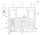
- FIG. 2 is a schematic plan view showing the resin molding system.
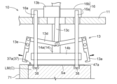
- FIG. FIG. 2 is a schematic front view showing a loader.
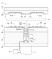
- 10 is a cross-sectional view showing the movement of a loader when the pre-molded substrate is placed on a lower mold.
- 10 is a cross-sectional view showing the movement of a loader when the pre-molded substrate is placed on a lower mold.
- 10 is a cross-sectional view showing the movement of a loader when the pre-molded substrate is placed on a lower mold.
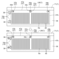
- 11 is a schematic diagram showing the movement of the pushing mechanism when the pre-molded substrate is positioned relative to the lower mold.
- Substrates with semiconductor chips etc. fixed on them can be resin-sealed to be used as electronic components.
- Techniques for resin-sealing molding objects include the transfer method.
- One transfer method involves supplying a release film to the upper die of a molding mold, placing the molding object on the lower die, supplying a resin tablet of solidified powdered resin to the mold pot, heating and melting it, and supplying the molten resin into the cavity to resin-mold the molding object.
- the resin tablet is made of a solid resin made by compressing powdered resin into a solid form, which melts when heated to become a liquid molten resin.
- the resin tablet may be a thermoplastic resin or a thermosetting resin.
- Thermosetting resin reduces in viscosity when heated, and when heated further, it polymerizes and hardens to become a hardened resin.
- a pre-molded substrate to which a semiconductor chip or the like is fixed is resin molded and sealed, it is desirable to use a thermosetting resin.
- FIG. 1 shows a schematic plan view of the resin molding system 30 in this embodiment.
- the resin molding system 30 includes a storage module 2, a molding module 3, a supply module 4, a control unit 6, a loader 10 (an example of a conveying device), and an unloader 42.
- the molding module 3 is a part that resin-seals the molding object, and has a molding die C that holds a pre-molded substrate Sa (an example of a molding object).
- the molding die C has an upper die UM and a lower die LM.
- the resin molding system 30 in this embodiment is an apparatus that resin-moldes a pre-molded substrate Sa to which a semiconductor chip 48 is fixed.
- the supply module 4 is for supplying pre-molded substrates Sa and resin tablets T (an example of a resin material) to the molding module 3, and includes a substrate supply mechanism 43 and a resin supply mechanism 45.
- the substrate supply mechanism 43 stocks pre-molded substrates Sa, and arranges the pre-molded substrates Sa in a state suitable for transport.
- a plurality of semiconductor chips 48 are fixed to the pre-molded substrate Sa, aligned vertically and/or horizontally.
- the resin supply mechanism 45 stocks resin tablets T, and arranges the resin tablets T in a state suitable for transport.
- the pre-molded substrate Sa may have one semiconductor chip 48 fixed thereto.
- the loader 10 waits in the supply module 4.
- the loader 10 receives the pre-molded substrate Sa from the substrate supply mechanism 43, and also receives the resin tablet T from the resin supply mechanism 45, and moves from the supply module 4 to the molding module 3 on rails (not shown) arranged on the rear side (upper side in FIG. 1) from the supply module 4 to the molding module 3.
- the loader 10 then transfers the pre-molded substrate Sa and the resin tablet T to the lower mold LM of the molding module 3.
- the loader 10 then moves again on the rails to the supply module 4.
- the molding module 3 uses a molding die C to resin-seal the pre-molded substrate Sa to form a molded substrate Sb (an example of a resin molded product).
- a molding die C to resin-seal the pre-molded substrate Sa to form a molded substrate Sb (an example of a resin molded product).
- one molding module 3 is provided, but two or more may be provided. When two or more molding modules are provided, each molding module 3 can be attached or detached independently.
- the storage module 2 has a substrate storage section 46.
- the unloader 42 waits in the storage module 2 and moves along rails (not shown) arranged on the rear side (upper side in FIG. 1) from the storage module 2 to the molding module 3 to remove the molded substrate Sb from the molding module 3, and then moves along the rails again to the storage module 2 to store the molded substrate Sb in the substrate storage section 46.
- the semiconductor chip 48 is sealed with a cured resin formed by solidifying molten resin Ta (an example of a resin material).
- the control unit 6 includes a processor such as a CPU (Central Processing Unit) and a storage device such as a RAM (Random Access Memory).
- the control unit 6 controls the operation of the resin molding system 30 by executing a control program stored in the storage device with the processor.
- the operation of the resin molding system 30 described below is performed based on operation commands from the control unit 6 unless otherwise specified. In the following description, explanations of the operation commands from the control unit 6 will be omitted as a general rule, and the operation commands from the control unit 6 will be explained as necessary.
- the resin molding system 30 of the molding module 3 is described in detail below.
- the molding module 3 has a lower mold LM of a molding die C provided with a transfer mechanism 72, an upper mold UM that is provided opposite the lower mold LM and has an upper mold cavity MCa formed therein into which molten resin Ta is injected, and a clamping mechanism 5 that clamps the lower mold LM and the upper mold UM.
- the lower mold LM is provided via a lower mold holder 34 on a movable platen 35 that is raised and lowered by the clamping mechanism 5.
- the upper mold UM is provided via an upper platen 32 on an upper fixed platen (not shown).
- the clamping mechanism 5 can be, for example, a combination of a servo motor and a ball screw mechanism, or a combination of an air cylinder or hydraulic cylinder and a rod.
- one pre-molded substrate Sa is placed on each side of the pot block 71 of the lower die LM, and two pre-molded substrates Sa are resin molded in one resin molding operation, but this is not particularly limited to this configuration, and one pre-molded substrate Sa may be resin molded in one resin molding operation.
- the operation of the mold clamping mechanism 5 is controlled by the control unit 6.
- the pre-molded substrate Sa is transported between the upper die UM and the lower die LM by the loader 10, and then placed on the lower die LM.
- a release film F is placed on the upper die UM in which the upper die cavity MCa is formed.
- the material used for the release film F is a resin material that has properties such as heat resistance, releasability, flexibility, and extensibility, and examples of such materials include PTFE (polytetrafluoroethylene), ETFE (ethylene/tetrafluoroethylene copolymer), PET (polyethylene terephthalate), FEP (tetrafluoroethylene/hexafluoropropylene copolymer), polypropylene, polystyrene, and polyvinylidene chloride.
- PTFE polytetrafluoroethylene
- ETFE ethylene/tetrafluoroethylene copolymer
- PET polyethylene terephthalate
- FEP tetrafluoroethylene/hexafluoropropylene copolymer
- polypropylene polystyrene
- polystyrene polystyrene
- polyvinylidene chloride polyvinylidene chloride
- the resin injection mechanism 7 includes a pot block 71 in which a pot 71a that contains a resin tablet T is formed, and a transfer mechanism 72 having a plunger 72a provided in the pot 71a.
- the transfer mechanism 72 includes a plunger 72a and a plunger drive mechanism 72c that drives the plunger 72a.
- the plunger 72a pumps out the molten resin Ta that is produced when the resin tablet T contained in the pot 71a is heated and melted.
- the operation of the plunger drive mechanism 72c is controlled by the control unit 6.
- the plunger drive mechanism 72c moves the multiple plungers 72a up and down collectively with respect to the multiple pots 71a by the same amount of movement.
- the plunger drive mechanism 72c is provided below the plungers 72a.
- the plunger drive mechanism 72c may be a combination of a servo motor and a ball screw mechanism, or a combination of an air cylinder or hydraulic cylinder and a rod.
- the pot block 71 is positioned so that it is at the same height as the pre-molded substrate Sa when the pre-molded substrate Sa is placed on the lower mold LM. In other words, the end surface 71b of the pot block 71 protrudes further toward the upper mold UM than the top surface 36 of the lower mold LM.
- the upper mold UM has an upper mold cavity MCa that houses the semiconductor chip 48 fixed to the pre-molding substrate Sa and into which the molten resin Ta is injected.
- the upper mold UM also has a cull portion 81, which is a recess, formed in the portion facing the pot 71a, and a runner portion 82 that connects the cull portion 81 to the upper mold cavity MCa.
- the upper mold UM has an air vent (not shown) formed on the opposite side of the upper mold cavity MCa to the pot 71a.
- the resin flow path formed by the cull portion 81 and runner portion 82 connects the multiple pots 71a to the upper mold cavity MCa.
- the pre-molded substrate Sa is sandwiched between the bottom surface of the upper mold UM and the top surface 36 of the lower mold LM.
- the plunger 72a is raised by the plunger drive mechanism 72c to inject molten resin Ta into the upper mold cavity MCa, and the semiconductor chip 48 of the pre-molded substrate Sa is resin-sealed.
- positioning pins 37 are arranged toward the upper mold UM.
- the three positioning pins 37 are arranged on the upper surface 36 of the lower mold LM. More specifically, one of the three positioning pins 37 is arranged on the side closer to the pot block 71 with respect to the upper mold cavity MCa, in the center of the upper surface 36 of the lower mold LM. The other two are arranged along the pot block 71, sandwiching the one positioning pin 37 arranged in the center of the upper surface 36 of the lower mold LM.
- Each of the three positioning pins 37 is, for example, a cylindrical shape (with a circular cross section) with a diameter of 1.5 mm and a height of 1.5 mm.
- Each of the three positioning pins 37 has a pin shape with a C-chamfered tip, and the tip is pointed.
- first positioning pin 37a an example of a positioning portion
- second positioning pins 37b the two positioning pins 37 arranged to sandwich the first positioning pin 37a
- positioning pins 37 When there is no need to distinguish between the one first positioning pin 37a and the two second positioning pins 37b, they are simply referred to as positioning pins 37.
- the three positioning pins 37 are passed through each of a plurality of positioning holes 49 (three in this embodiment) formed on the outer edge of the pre-molded substrate Sa, thereby positioning the pre-molded substrate Sa relative to the lower mold LM.
- the positioning pins 37 may be stepped pins that include a thick large diameter portion at the bottom and a thin small diameter portion at the top.
- the one positioning hole 49 through which the first positioning pin 37a passes is referred to as the first positioning hole 49a (an example of a positioning hole), and the two positioning holes 49 through which the second positioning pin 37b passes are referred to as the second positioning holes 49b (see Figure 7).
- the plate surface of the pre-molded substrate Sa is rectangular.
- the two sides that run along the arrangement direction of the three positioning holes 49 are referred to as the long sides 47a, and the two sides perpendicular to the long sides 47a are referred to as the short sides 47b.
- the first positioning hole 49a is square-shaped when viewed along a direction perpendicular to the plate surface of the pre-molded substrate Sa (a direction perpendicular to the upper surface 36 of the lower mold LM when the pre-molded substrate Sa is placed on the lower mold LM), and each side (each inner surface) of the first positioning hole 49a is parallel to the long side 47a and the short side 47b of the pre-molded substrate Sa.
- the second positioning hole 49b has a shape in which two sides parallel to the long side 47a are connected by a concave curve (e.g., a circular arc) in which one end of each of the two sides and the other end of each of the two sides bulge outward relative to the two parallel sides.
- the distance between the two parallel sides of the second positioning hole 49b is such that the second positioning pin 37b can be inserted without any gaps (e.g., a little more than 1.5 mm).
- the distance between the two opposing sides of the first positioning hole 49a is greater than that (e.g., 1.8 mm).
- the direction parallel to the long side 47a of the pre-molded substrate Sa is referred to as the longitudinal direction
- the direction parallel to the short side 47b is referred to as the short direction.
- the shape of the first positioning hole 49a when viewed along a direction perpendicular to the plate surface of the pre-molded substrate Sa may be rectangular, as long as each side is parallel to the long side 47a and short side 47b of the pre-molded substrate Sa.
- the molding die C in this embodiment is a molding die C that resin molds two pre-molded substrates Sa by one resin molding operation, so that the same configuration is provided for the other of the two pre-molded substrates Sa (see Fig. 2) placed on both sides of the lower mold LM with the pot block 71 in between in the portion of the base member 11 shown by the omitted lines in Figs. 3 to 6.
- the loader 10 includes a base member 11 that is movable along a rail (not shown), and a base member lifting and moving mechanism (not shown) that moves the base member 11 up and down.
- the base member 11 includes a substrate holding section 13 that holds the pre-molded substrate Sa, a pressing section 14 that presses down the pre-molded substrate Sa placed on the lower mold LM, a shifting mechanism 16 that positions the pre-molded substrate Sa, and a pressing section lifting and moving mechanism (not shown) that moves the pressing section 14 up and down.
- the base member 11 also includes a resin holding section (not shown) that holds a resin tablet T.
- the board holding part 13 has a holding claw 13a, a drive part 13b, a lever 13c, a link 13d, and a shaft 13e.
- the holding claws 13a in this embodiment are for holding the pre-molded substrate Sa in the loader 10 by hooking the opposing long sides 47a of the rectangular pre-molded substrate Sa (see FIG. 4).
- a plurality of holding claws 13a (four in this embodiment) are arranged at the end on the pot 71a side, and a plurality of holding claws 13a (four in this embodiment) are arranged at the end opposite the end on the pot 71a side.
- the holding claws 13a are configured to be openable and closable by swinging about the shaft 13e. When the holding claws 13a are closed, they hook the long sides 47a of the pre-molded substrate Sa to hold the pre-molded substrate Sa in the loader 10.
- the pre-molded substrate Sa is released from the hook and the pre-molded substrate Sa is released from the hold.
- the released pre-molded substrate Sa falls from the loader 10 and is placed on the mold surface of the lower mold LM (see FIG. 5).
- the drive unit 13b is, for example, an air cylinder, and can move the lever 13c up and down.
- the lever 13c connects the drive unit 13b to a link 13d.
- the link 13d connects the lever 13c to the retaining claw 13a, and is configured to be able to swing relative to the lever 13c and the retaining claw 13a.
- the shaft 13e passes through the multiple retaining claws 13a arranged at the pot side end and the multiple retaining claws 13a arranged at the opposite end, and serves as a swing fulcrum for the retaining claw 13a.
- the pressing portion 14 is arranged to press the pre-molded substrate Sa, which is placed on the lower mold LM with the positioning pins 37 formed on the lower mold LM passing through the positioning holes 49, toward the lower mold LM by pressing the outer edge of the pre-molded substrate Sa toward the lower mold LM.
- the pressing member 14b is connected to the two connecting shafts 14a, and moves up and down (up and down) together with the connecting shafts 14a.
- both of the two connecting shafts 14a pass through the base member 11, and are connected to each other above the base member 11.
- the pre-molded substrate Sa is held by being sandwiched between the holding claws 13a of the substrate holding portion 13 and the pressing portion 14.
- the pressing portion 14 includes a pressing member 14b.
- the pressing member 14b is formed in a frame shape so that it can press the outer edge of the pre-molded substrate Sa toward the lower mold LM.
- the inside of the frame is recessed, and the semiconductor chip 48 fixed to the pre-molded substrate Sa is disposed in the recess.
- the lifting and lowering mechanism (not shown) adjusts the height position of the holding part 14 relative to the base member 11.
- the lifting and lowering mechanism is composed of an air cylinder or the like.
- the lifting and lowering mechanism can change the height position of the holding part 14 relative to the base member 11 by lifting and lowering the connecting shaft 14a relative to the base member 11.
- the shifting mechanism 16 is a mechanism that positions the pre-molded substrate Sa relative to the lower mold LM by pushing the pre-molded substrate Sa placed on the lower mold LM.
- the shifting mechanism 16 includes a substrate pushing section 16a (an example of a molding object pushing section) that pushes the short side 47b of the pre-molded substrate Sa, and a drive section 16b that drives the substrate pushing section 16a.
- the shifting mechanism 16 is controlled by the control section 6.
- the drive unit 16b is an electric actuator and is disposed on the base member 11.
- the board pressing units 16a are a pair of rod-shaped members, one end of which is attached to the drive unit 16b and extends through the base member 11.
- the other end of the board pressing units 16a is located below the upper surface 36 of the lower mold LM.
- Each of the pair of board pressing units 16a is disposed so as to press both ends (near the long side 47a) of one of the short sides 47b of the pre-molded substrate Sa, and they move in the same manner at the same time due to the drive unit 16b.
- the portion of the board pressing units 16a facing the short side 47b of the pre-molded substrate Sa is curved (see FIG. 7).
- the lower mold LM is formed with a pair of grooves 38 to avoid interference with the other ends of the pair of board pressing units 16a.
- the manufacturing method according to this embodiment includes a substrate supplying process (an example of a supplying process) in which the pre-molded substrate Sa, which has been released from the substrate holding section 13 of the loader 10, is placed on the lower mold LM so that the positioning pin 37 of the lower mold LM passes through the positioning hole 49, and then the first positioning pin 37a is pushed by the moving mechanism 16 until it contacts the contact surface 49c (an example of a surface) of the first positioning hole 49a to position the pre-molded substrate Sa and supply a resin tablet T, a mold clamping process in which the mold clamping mechanism 5 clamps the mold C, and a molding process in which molten resin Ta is supplied to the upper mold cavity MCa to perform resin molding of the pre-molded substrate Sa.
- the contact surface 49c of the first positioning hole 49a is flat.
- the molding process is a process in which the resin molding system 30 resin molds the pre-molded substrate Sa during the period from when the pre-molded substrate Sa is carried into the molding module 3 until when the molded substrate Sb is carried out from the molding module 3.
- molten resin Ta is supplied to the upper mold cavity MCa, and the molten resin Ta is supplied to the surface of the pre-molded substrate Sa to mold it and produce the molded substrate Sb.
- the semiconductor chip 48 fixed to the pre-molded substrate Sa is not shown in Figures 1 and 3 to 6.
- only one side (the right side in Figure 2) of the lower mold LM relative to the pot block 71 is shown in Figures 4 to 6.
- the configuration of the parts not shown is the same as the configuration of the parts shown.
- the upper mold UM is not shown in Figures 4 to 6.
- the loader 10 is heated in advance with the storage space for the resin tablets T insulated, and the mold C is also heated. Then, the pre-molded substrate Sa taken out from the substrate supply mechanism 43 is placed on the loader 10. Also, the resin tablets T aligned by the resin supply mechanism 45 are stored in the storage space for the resin tablets T of the loader 10. Then, the loader 10 transports the pre-molded substrate Sa and the resin tablets T to the molding module 3. The loader 10 places the pre-molded substrate Sa on the lower mold LM while being disposed between the upper mold UM and lower mold LM of the mold C, as shown by the two-dot chain line in FIG. 2. The placement of the pre-molded substrate Sa on the lower mold LM will be described in detail later.
- the release film F is supplied to the lower surface of the upper mold UM before the pre-molded substrate Sa is placed on the lower mold LM, and is adsorbed and fixed to the lower surface of the upper mold UM by a release film suction mechanism (not shown) provided on the upper mold UM (see FIG. 4). Note that FIG. 2 shows the state after the pre-molded substrate Sa has been placed on the lower mold LM.
- the control unit 6 uses a base member lifting and moving mechanism (not shown) to lower the base member 11 and the pressing unit 14 including the connecting shaft 14a.
- the substrate holding unit 13, pre-molded substrate Sa, and the pushing mechanism 16 also lower together with the base member 11.
- the end of the substrate pushing unit 16a of the pushing mechanism 16 enters the groove 38 of the lower mold LM.
- FIG. 4 shows the base member 11 in the lowered state. At this time, the pressing unit 14 is above the lower mold LM, and the pre-molded substrate Sa held by the loader 10 is not in contact with the upper surface 36 of the lower mold LM.
- the substrate holding unit 13 moves the lever 13c downward (toward the lower mold LM) by the drive unit 13b.
- the lever 13c moves downward, the end of the link 13d connected to the lever 13c moves downward.
- This causes the holding claw 13a connected to the other end of the link 13d to swing about the shaft 13e and open.
- the holding claw 13a opens, the pre-molded substrate Sa is released from the hook and the pre-molded substrate Sa is released from the hold.
- the released pre-molded substrate Sa falls from the loader 10 and is placed on the lower mold LM.
- the first positioning pin 37a arranged on the lower mold LM is passed through the first positioning hole 49a formed in the pre-molded substrate Sa
- the second positioning pin 37b arranged on the lower mold LM is passed through the second positioning hole 49b.
- the pressing unit lifting and moving mechanism lowers the pressing unit 14 including the connecting shaft 14a, and presses the pre-molded substrate Sa placed on the lower mold LM toward the lower mold LM. This ensures that the entire pre-molded substrate Sa comes into contact with the upper surface 36 of the lower mold LM.
- the pressing part 14 is raised to the state shown in FIG. 5 by the pressing part lifting and moving mechanism.
- the driving part 16b of the pushing mechanism 16 is driven to push one short side 47b of the pre-molded substrate Sa by the substrate pushing part 16a.
- the moving speed of the substrate pushing part 16a is initially set to a first moving speed, and is decelerated to a second moving speed slower than the first moving speed just before contacting the short side 47b of the pre-molded substrate Sa.
- the substrate pushing part 16a is brought into contact with the short side 47b of the pre-molded substrate Sa at the second moving speed to push the pre-molded substrate Sa until the first positioning pin 37a comes into contact with the contact surface 49c of the first positioning hole 49a formed in the pre-molded substrate Sa.
- the driving part 16b cannot push the substrate pushing part 16a any further, and the driving current flowing through the driving part 16b increases.
- the control unit 6 detects a drive current exceeding a predetermined value, it stops the supply of electricity to the drive unit 16b. Note that when the first positioning pin 37a contacts the contact surface 49c of the first positioning hole 49a, the two second positioning pins 37b are not in contact with the concave curved surface 49d of the second positioning hole 49b.
- the distance between the two parallel sides of the second positioning hole 49b is such that the second positioning pin 37b can be inserted without any gaps (e.g., just over 1.5 mm). Therefore, when the pre-molded substrate Sa is pushed by the pushing mechanism 16, the pre-molded substrate Sa can be moved along the longitudinal direction without moving or rotating in the lateral direction.
- the presser lifting and moving mechanism lowers the presser 14 including the connecting shaft 14a again, and presses the pre-molded substrate Sa placed on the lower mold LM toward the lower mold LM.
- the pre-molded substrate Sa is adsorbed and fixed to the upper surface 36 of the lower mold LM by a suction mechanism (not shown) provided in the lower mold LM.
- the loader 10 places the resin tablet T in the pot 71a of the lower mold LM while pressing the pre-molded substrate Sa against the mold surface of the lower mold LM with the pressing portion 14 (supply process).
- the heater built into the lower mold LM heats the resin tablet T, turning it into molten resin Ta.
- the pressing part 14 is raised again to the state shown in FIG. 5 by the pressing part lifting and moving mechanism.
- the pressing part 14 including the connecting shaft 14a is raised by the base member lifting and moving mechanism.
- the base member 11 rises, the substrate holding part 13 and the pushing mechanism 16 also rise.
- the end of the substrate pushing part 16a of the pushing mechanism 16 comes out of the groove 38 of the lower mold LM.
- the loader 10 then moves from between the upper mold UM and the lower mold LM to the outside of the molding mold C and returns to the supply module 4.
- the upper mold UM and the lower mold LM are moved closer to each other by the clamping mechanism 5, whose driving force is controlled by the control unit 6, and the upper mold UM and the lower mold LM are clamped together.
- the lower surface of the upper mold UM comes into contact with the peripheral portion of the surface of the pre-molded substrate Sa on which the semiconductor chip 48 is fixed, and the pre-molded substrate Sa is held by the lower mold LM and the upper mold UM (clamping process).
- the molten resin Ta produced by melting the resin tablet T contained in the lower mold LM is injected into the upper mold cavity MCa by the transfer mechanism 72, whose driving force is controlled by the control unit 6. This causes the pre-molding substrate Sa to be molded with resin (molding process). After the resin molding, the lower mold LM is moved downward to open the molding die C.
- the unloader 42 removes the unnecessary resin and the molded substrate Sb from the molding die C, the unnecessary resin is disposed of in an unnecessary resin storage section (not shown), and the molded substrate Sb is stored in the substrate storage section 46 of the storage module 2 (see FIG. 1).
- the package substrate (molded substrate Sb) manufactured by this resin molding system 30 is then cut into individual pieces by a cutting device, with unnecessary portions of the package substrate being removed, and the cut pieces are used as electronic components after undergoing quality inspection.
- the loader 10 has a pushing mechanism 16. Therefore, the pre-molded substrate Sa can be accurately positioned with respect to the lower mold LM. Specifically, the pre-molded substrate Sa placed on the lower mold LM is pushed by the substrate pushing part 16a, so that the first positioning pin 37a comes into contact with the contact surface 49c of the first positioning hole 49a to perform positioning.
- the first positioning pin 37a is cylindrical, and the surface facing the first positioning hole 49a is a convex curved surface, and the contact surface 49c of the first positioning hole 49a is flat, so that the first positioning pin 37a and the contact surface 49c contact each other at one point.
- This allows the positioning of the pre-molded substrate Sa to be performed with high precision. Therefore, for example, as shown in FIG. 7, even when resin sealing is performed on multiple rows of semiconductor chips 48 arranged at equal intervals along the longitudinal direction of the pre-molded substrate Sa, the pre-molded substrate Sa can be positioned with high precision in the longitudinal direction before resin sealing.
- an electric actuator is used as the drive unit 16b of the pushing mechanism 16. Since the electric actuator has high controllability, the position, moving speed, and pressing force of the board pushing unit 16a can be accurately controlled. Specifically, as described above, the moving speed of the board pushing unit 16a is decelerated just before contacting the short side 47b of the pre-molded board Sa, and the board pushing unit 16a is brought into contact with the short side 47b of the pre-molded board Sa at the low speed to push the pre-molded board Sa, and the first positioning pin 37a is brought into contact with the contact surface 49c of the first positioning hole 49a.
- the speed and position are controlled by the electric actuator, but the pressing force may also be controlled.
- the pressing force may be controlled from the start of control, or the speed and position may be controlled as in the above-described embodiment until halfway through, and then the control may be changed to pressing force just before the first positioning pin 37a contacts the contact surface 49c or at a certain position.
- the control unit 6 detects that the drive current flowing through the drive unit 16b has exceeded a predetermined value and stops the flow of electricity to the drive unit 16b, but this is not limited to the above. Since the drive unit 16b uses an electric actuator with high controllability, the control unit 6 may be configured to stop the flow of electricity to the drive unit 16b when it detects that the board pushing unit 16a has reached a position where the first positioning pin 37a contacts the contact surface 49c of the first positioning hole 49a.
- the control unit 6 detects that the drive current flowing through the drive unit 16b has exceeded a predetermined value and stops the supply of electricity to the drive unit 16b, but at this time, there is a possibility that the first positioning pin 37a is not in contact with the contact surface 49c of the first positioning hole 49a. Specifically, for example, this is the case when the drive current flowing through the drive unit 16b exceeds the predetermined value due to at least one positioning pin 37 getting caught on the inner surface of the positioning hole 49 before the first positioning pin 37a contacts the contact surface 49c of the first positioning hole 49a.
- control unit 6 may be configured to detect that the drive current flowing through the drive unit 16b has first exceeded the predetermined value, stop the supply of electricity to the drive unit 16b, and then supply electricity to the drive unit 16b again. Immediately after current is applied again to the drive unit 16b, the output torque of the drive unit 16b increases, so the substrate pushing unit 16a can overcome the snag and push the pre-molded substrate Sa again until the first positioning pin 37a comes into contact with the contact surface 49c of the first positioning hole 49a.
- the positioning holes 49 are arranged along the long side 47a of the pre-molded substrate Sa, but if it is necessary to perform positioning in the direction of the short side 47b with high precision, multiple positioning holes 49 may be arranged along the short side 47b, and the pushing mechanism 16 may be arranged so that the pre-molded substrate Sa can be pushed in the direction along the short side 47b.
- the plate surface of the pre-molded substrate Sa is rectangular, but this is not limited to this and any shape, such as a circle, can be applied.
- a plurality of positioning holes 49 may be arranged along the direction in which positioning accuracy is required, and a pushing mechanism 16 may be provided.
- the first positioning hole 49a is square or rectangular when viewed along a direction perpendicular to the plate surface of the pre-molding substrate Sa, but is not limited to this.
- the shape of other parts may be any shape, such as a curved surface.
- the first positioning pin 37a may have any shape, such as an elliptical shape, in a cross section perpendicular to the height direction, as long as the part of the first positioning hole 49a that contacts the contact surface 49c of the first positioning hole 49a is a convex curved surface.
- the first positioning hole 49a and the first positioning pin 37a contact each other at a flat surface and a convex curved surface
- the first positioning hole 49a may be a convex curved surface and the first positioning pin 37a may be a flat surface.
- the distance between the two parallel sides of the second positioning hole 49b is set to a value that allows the second positioning pin 37b to fit in without any gaps (e.g., just over 1.5 mm), but this is not limited to this.
- the distance between the two parallel sides of the second positioning hole 49b may be set to 1.5 mm to set the clearance with the second positioning pin 37b to zero.
- the length of the first positioning hole 49a in the direction along the short side 47b may be set to 1.5 mm to set the clearance with the first positioning pin 37a to zero.
- the positioning pin 37 is disposed on the side closer to the pot block 71 than the upper die cavity MCa, but this is not limited to this.
- the positioning pin 37 may also be configured to be disposed on the side farther from the pot block 71 than the cavity.
- the resin tablet T is accommodated in the pot 71a of the lower mold LM when the pressing unit 14 presses the pre-molded substrate Sa toward the lower mold LM for the second time, but this is not limited to the above.
- the resin tablet T may be accommodated in the pot 71a of the lower mold LM when the pressing unit 14 presses the pre-molded substrate Sa toward the lower mold LM for the first time.
- the resin tablet T may be accommodated in the pot 71a of the lower mold LM when the pressing unit 14 presses the pre-molded substrate Sa against the lower mold LM and the pressing unit 14 is raised from the pre-molded substrate Sa.
- the movement speed of the substrate pushing unit 16a is initially set to a first movement speed, and is then reduced to a second movement speed slower than the first movement speed just before contacting the short side 47b of the pre-molded substrate Sa, but this is not limited to this.
- the movement speed of the substrate pushing unit 16a may be constant as long as the contact surface 49c is not deformed when it is brought into contact with the contact surface 49c of the first positioning hole 49a, or the molding time of the pre-molded substrate Sa is not excessive.
- the movement speed of the substrate pushing unit 16a may also be configured to be changed in three or more stages.
- the resin injection mechanism 7 clamps the pre-molded substrate Sa placed on the lower mold LM between the upper mold UM to perform resin molding, and the molten resin Ta supplied from the pot 71a passes through the end of the pre-molded substrate Sa and is supplied to the upper mold cavity MCa (sometimes called the side gate method).
- the resin injection mechanism 7 may clamp the pre-molded substrate Sa placed on the lower mold LM between the lower mold LM and the protruding part of the pot block to perform resin molding, and the molten resin Ta supplied from the pot 71a is supplied to the cavity without passing through the end of the pre-molded substrate Sa (sometimes called the edge gate method).
- the pre-molded substrate Sa can be positioned relative to the lower mold LM by the alignment mechanism 16 before the mold C is clamped.
- the mold C may be equipped with an intermediate mold in addition to the lower mold LM and upper mold UM, and unnecessary resin may be removed by the intermediate mold when the mold is opened after resin molding (sometimes called the top gate method).
- the molten resin Ta was supplied to only one side of the pre-molding substrate Sa to perform single-sided molding, but double-sided molding may be performed by injecting the molten resin Ta into not only the upper mold cavity MCa provided in the upper mold UM, but also a lower mold cavity provided in the lower mold LM.
- the pushing mechanism 16 is applied to a transfer type resin molding system 30, but it can also be applied when the pre-molded substrate Sa is placed on the lower mold LM in a compression type resin molding system 30.
- the pre-molded substrate Sa is constructed by fixing the semiconductor chip 48 to the substrate, but this is not limited to this.
- any type of chip such as a resistor element or a capacitor element, may be fixed to the substrate to construct the pre-molded substrate Sa.
- the substrate used for the pre-molded substrate Sa that is resin molded by the resin molding system 30 in the above-described embodiment is, for example, a semiconductor substrate (such as a silicon wafer), a metal substrate (such as a lead frame), a glass substrate, a ceramic substrate, a resin substrate, or a printed wiring substrate, and also includes carriers that are not wired.
- the characteristic configuration of the resin molding system 30 is that it includes a mold C having a positioning section (first positioning pin 37a) that positions the molding object (pre-molded substrate Sa) having a positioning hole (first positioning hole 49a), on which the molding object (pre-molded substrate Sa) is placed with the positioning section (first positioning pin 37a) passing through the positioning hole (first positioning hole 49a), and a transport device (loader 10) having a pushing mechanism 16 that positions the molding object (pre-molded substrate Sa) relative to the positioning section (first positioning pin 37a) by bringing the positioning hole (first positioning hole 49a) into contact with the positioning section (first positioning pin 37a).
- the resin molding system 30 according to this characteristic configuration has a pushing mechanism 16. Therefore, in a state where the positioning portion (first positioning pin 37a) formed in the mold C is passed through the positioning hole (first positioning hole 49a) formed in the molding object (pre-molded substrate Sa), the pushing mechanism 16 pushes the molding object (pre-molded substrate Sa) to bring the positioning hole (first positioning hole 49a) into contact with the positioning portion (first positioning pin 37a).
- This simple method allows the molding object (pre-molded substrate Sa) to be positioned with high precision relative to the positioning portion (first positioning pin 37a).
- the pushing mechanism 16 does not press down on the molding object (pre-molded substrate Sa)
- the molding object (pre-molded substrate Sa) is not deformed. Therefore, when the molding object (pre-molded substrate Sa) is a carrier, the molding object (pre-molded substrate Sa) can be reused.
- the resin molding system 30 described in (1) above further includes a control unit 6 that controls the pushing mechanism 16, and the pushing mechanism 16 may have a molding object pushing section (substrate pushing section 16a) that pushes the molding object (pre-molding substrate Sa) and a drive section 16b that moves the molding object pushing section (substrate pushing section 16a).
- the pushing mechanism 16 may have a molding object pushing section (substrate pushing section 16a) that pushes the molding object (pre-molding substrate Sa) and a drive section 16b that moves the molding object pushing section (substrate pushing section 16a).
- control unit 6 controls the molding object pushing unit (substrate pushing unit 16a) and the drive unit 16b, so that the molding object (pre-molded substrate Sa) can be pushed by the molding object pushing unit (substrate pushing unit 16a), thereby enabling the molding object (pre-molded substrate Sa) to be positioned with high precision.
- control unit 6 may control the drive unit 16b to move the molding object pushing unit (substrate pushing unit 16a) close to the molding object (pre-molding substrate Sa) at a first moving speed, slow down to a second moving speed slower than the first moving speed just before contacting the molding object (pre-molding substrate Sa), and then contact the molding object (pre-molding substrate Sa) at the second moving speed to perform positioning.
- the control unit 6 controls the object to be molded (substrate pushing unit 16a) to approach the object to be molded (pre-molded substrate Sa) at a first moving speed, slow down to a second moving speed slower than the first moving speed just before contacting the object to be molded (pre-molded substrate Sa), and contact the object to be molded (pre-molded substrate Sa) at the second moving speed to perform positioning. Therefore, there is no risk of the positioning hole (first positioning hole 49a) being deformed when the positioning unit (first positioning pin 37a) is brought into contact with the positioning hole (first positioning hole 49a). Furthermore, the molding time of the object to be molded (pre-molded substrate Sa) can be shortened compared to when the object to be molded (substrate pushing unit 16a) is moved only at the slow second moving speed.
- control unit 6 may control the drive unit 16b to perform speed control up to a position just before contacting the molding object (pre-molding substrate Sa), and to perform pressing force control at a position just before contacting the molding object (pre-molding substrate Sa) to perform positioning.
- the control unit 6 controls the pressing force at a position just before contacting the object to be molded (pre-molded substrate Sa), for example to a pressing force of a magnitude that does not cause deformation of the object to be molded (pre-molded substrate Sa). This makes it possible to shorten the time until the positioning unit (first positioning pin 37a) comes into contact with the object to be molded (pre-molded substrate Sa) without deforming the object to be molded (pre-molded substrate Sa), and thus shorten the time required for resin molding.
- the drive unit 16b may be an electric actuator
- the control unit 6 may stop the movement of the molding object pushing unit (substrate pushing unit 16a) by stopping the flow of electricity to the electric actuator when the driving current of the electric actuator exceeds a predetermined value.
- the molding object pushing section (substrate pushing section 16a) cannot push the molding object (pre-molded substrate Sa) any further, and the drive current of the electric actuator increases. Therefore, with this configuration, the control section 6 stops the flow of electricity to the electric actuator when the drive current of the electric actuator exceeds a predetermined value, thereby enabling the positioning of the molding object (pre-molded substrate Sa) to be performed with high precision without deforming the positioning hole (first positioning hole 49a).
- control unit 6 may stop supplying current to the electric actuator when the drive current of the electric actuator exceeds a predetermined value, and then may supply current to the electric actuator again.
- the positioning section (first positioning pin 37a) may get caught on the inner surface of the positioning hole (first positioning hole 49a), causing the drive current flowing through the drive section 16b to exceed a predetermined value.
- the control section 6 temporarily stops driving the drive section 16b, but with this configuration, by subsequently passing current through the drive section 16b again, the object to be molded (pre-molded substrate Sa) can be pressed until the positioning hole (first positioning hole 49a) comes into contact with the positioning section (first positioning pin 37a).
- the positioning portion (first positioning pin 37a) is a pin having a circular cross section, and at least the surface (contact surface 49c) of the positioning hole (first positioning hole 49a) that contacts the positioning portion (first positioning pin 37a) is flat.
- the positioning portion (first positioning pin 37a) and the contact surface 49c of the positioning hole (first positioning hole 49a) come into contact at one point, so the object to be molded (pre-molding substrate Sa) can be positioned with high precision relative to the molding die C.
- the positioning hole (first positioning hole 49a) may be rectangular when viewed along a direction perpendicular to the surface (upper surface 36) of the mold C on which the molding object (pre-molding substrate Sa) is placed.
- pre-molded substrate Sa pre-molded substrate Sa
- the manufacturing method of a resin molded product (molded substrate Sb) using the resin molding system 30 described in any one of (1) to (8) above is characterized in that it includes a supply process in which the molding object (pre-molded substrate Sa) is placed on the molding mold C so that the positioning portion (first positioning pin 37a) passes through the positioning hole (first positioning hole 49a), and then the positioning hole (first positioning hole 49a) is brought into contact with the positioning portion (first positioning pin 37a) by the alignment mechanism 16 to position the molding object (pre-molded substrate Sa) relative to the positioning portion (first positioning pin 37a) and a resin material (resin tablet T, molten resin Ta) is supplied; a mold clamping process in which the mold C is clamped by the mold clamping mechanism 5; and a molding process in which the molding object (pre-molded substrate Sa) is resin molded.
- a supply process in which the molding object (pre-molded substrate Sa) is placed on the molding mold C so that the positioning portion (first positioning pin 37a) passes through the positioning hole (first positioning hole
- the molding object (pre-molded substrate Sa) is placed on the molding die C so that the positioning portion (first positioning pin 37a) passes through the positioning hole (first positioning hole 49a), and then the positioning hole (first positioning hole 49a) is brought into contact with the positioning portion (first positioning pin 37a) by the alignment mechanism 16 to position the molding object (pre-molded substrate Sa) relative to the positioning portion (first positioning pin 37a) and a supply process is performed to supply a resin material (resin tablet T, molten resin Ta), a mold clamping process is performed to clamp the molding die C by the mold clamping mechanism 5, and a molding process is performed to mold the molding object (pre-molded substrate Sa) into resin is performed to manufacture the resin molded product (molded substrate Sb).
- a resin material resin tablet T, molten resin Ta
- a mold clamping process is performed to clamp the molding die C by the mold clamping mechanism 5
- a molding process is performed to mold the molding object (pre-molded substrate Sa) into resin is performed to manufacture the resin molded product (molded substrate Sb
- the resin molded product (molded substrate Sb) can be manufactured in a state in which the molding object (pre-molded substrate Sa) is positioned with high precision relative to the molding die C, and therefore the resin molded product (molded substrate Sb) can be manufactured with high precision using the molding die C.
- This disclosure can be used in resin molding systems and methods for manufacturing resin molded products.
- Mold clamping mechanism 6 Control unit 10: Loader (transport device) 16: Pushing mechanism 16a: Substrate pushing section (molding object pushing section) 16b: Drive unit 30: Resin molding system 36: Top surface (surface) 37a: First positioning pin (positioning portion) 49a: First positioning hole (positioning hole) 49c: Contact surface (surface) C: Mold Sa: Pre-molded substrate (molding object) Sb: Molded substrate (resin molded product) T: Resin tablet (resin material) Ta: Molten resin (resin material)
Landscapes
- Engineering & Computer Science (AREA)
- Mechanical Engineering (AREA)
- Manufacturing & Machinery (AREA)
- Moulds For Moulding Plastics Or The Like (AREA)
- Encapsulation Of And Coatings For Semiconductor Or Solid State Devices (AREA)
- Injection Moulding Of Plastics Or The Like (AREA)
Abstract
樹脂成形システムは、位置決め孔(49a)を有する成形対象物(Sa)の位置決めを行う位置決め部(37a)を有し、位置決め部(37a)が位置決め孔(49a)に通された状態で成形対象物(Sa)が載置される成形型(C)と、位置決め孔(49a)を位置決め部(37a)に接触させることにより、成形対象物(Sa)の位置決め部(37a)に対する位置決めを行う寄せ機構(16)を有する搬送装置と、を備えている。
Description
本開示は、樹脂成形システム及び樹脂成形品の製造方法に関する。
半導体チップ等が固定された基板は、一般的に樹脂封止することにより電子部品として用いられる。従来、基板等を樹脂封止するための樹脂成形システムとして成形型を備えたものが知られている(例えば、特許文献1参照)。
特許文献1には上型と下型とを含む成形型を有する樹脂成形システム(特許文献1では半導体装置)が開示されている。特許文献1の樹脂成形システムでは、下型に対して基板を位置決めする構成について記載されている。基板は、その長手方向の中央部に基準点となる円形の開口形状を有する主位置決め孔(特許文献1では孔部)と、長手方向における主位置決め孔の両側に細長く形成された開口形状を有する2つの副位置決め孔とを備えている。下型は、基板の3つの位置決め孔に対応する、円形の平面外形を有する3つの位置決め部(特許文献1ではピン)を有している。そして、3つの位置決め孔に対応する3つの位置決め部が通されることにより、下型に対して基板が位置決めされる。特に、主位置決め孔と対応する位置決め部とにより、基板の位置決めがなされる。
特許文献1に記載の樹脂成形システムにおいては、下型に基板を載置しやすくするため、主位置決め孔の内径を、対応する位置決め部の外径よりも若干大きくしている。また、基板の短手方向に沿う副位置決め孔の細長く形成された開口の長さは主位置決め孔の内径よりも大きい。そのため、基板を下型に載置した状態、すなわち、位置決め部が主位置決め孔に通された状態であっても、基板は下型に対してあらゆる方向に僅かに移動可能となり、半導体チップの種類によっては、必要な位置決め精度が得られないおそれがある。
そこで、成形型に対する基板の位置決めを高精度に行うことができる樹脂成形システム及び樹脂成形品の製造方法が望まれている。
本開示に係る樹脂成形システムの一つの実施形態は、位置決め孔を有する成形対象物の位置決めを行う位置決め部を有し、前記位置決め部が前記位置決め孔に通された状態で前記成形対象物が載置される成形型と、前記位置決め孔を前記位置決め部に接触させることにより、前記成形対象物の前記位置決め部に対する位置決めを行う寄せ機構を有する搬送装置と、を備えている。
本開示に係る樹脂成形品の製造方法の一つの実施形態は、上記に記載の樹脂成形システムを用いた樹脂成形品の製造方法であって、前記位置決め部が前記位置決め孔に通るように前記成形対象物を前記成形型に載置した後、前記寄せ機構により前記位置決め孔を前記位置決め部に接触させて前記成形対象物の前記位置決め部に対する位置決めを行うと共に樹脂材料を供給する供給工程と、型締め機構により前記成形型を型締めする型締め工程と、前記成形対象物の樹脂成形を行う成形工程と、を含んでいる。
本開示の実施形態によれば、成形型に対する基板の位置決めを高精度に行うことができる樹脂成形システム及び樹脂成形品の製造方法を提供することができる。
以下に、本開示に係る樹脂成形システム及び樹脂成形品の製造方法の実施形態について、図面に基づいて説明する。ただし、本開示は、以下の実施形態に限定されることなく、その要旨を逸脱しない範囲内で種々の変形が可能である。
半導体チップ等が固定された基板(成形対象物)は樹脂封止することにより電子部品として用いられる。成形対象物を樹脂封止する技術としては、トランスファ方式等が挙げられる。トランスファ方式の一つとして、成形型の上型に離型フィルムを供給し、下型に成形対象物を載置し、成形型のポットに粉粒体状樹脂を固めた樹脂タブレットを供給して加熱、溶融し、溶融樹脂をキャビティに供給して成形対象物を樹脂成形する方式が挙げられる。
樹脂タブレットは、粉粒体状の樹脂を押し固めた固形樹脂で形成され、加熱により溶融して液状の溶融樹脂となる。樹脂タブレットは、熱可塑性樹脂でも熱硬化性樹脂でもよい。熱硬化性樹脂は、加熱すると粘度が低下し、さらに加熱すると重合して硬化し、硬化樹脂となる。以下に説明するように、半導体チップ等が固定された成形前基板を樹脂成形して封止する場合には、熱硬化性樹脂を用いることが望ましい。
〔全体構成〕
以下、トランスファ方式の樹脂成形システム30を一例として説明する。図1には、本実施形態における樹脂成形システム30の平面模式図が示されている。樹脂成形システム30は、収容モジュール2、成形モジュール3、供給モジュール4、制御部6、ローダ10(搬送装置の一例)、及びアンローダ42を備えている。成形モジュール3は、成形対象物を樹脂封止する部分であり、成形前基板Sa(成形対象物の一例)を保持する成形型Cを有している。成形型Cは上型UMと下型LMとを有する。本実施形態における樹脂成形システム30は、半導体チップ48が固定された成形前基板Saを樹脂成形する装置である。
以下、トランスファ方式の樹脂成形システム30を一例として説明する。図1には、本実施形態における樹脂成形システム30の平面模式図が示されている。樹脂成形システム30は、収容モジュール2、成形モジュール3、供給モジュール4、制御部6、ローダ10(搬送装置の一例)、及びアンローダ42を備えている。成形モジュール3は、成形対象物を樹脂封止する部分であり、成形前基板Sa(成形対象物の一例)を保持する成形型Cを有している。成形型Cは上型UMと下型LMとを有する。本実施形態における樹脂成形システム30は、半導体チップ48が固定された成形前基板Saを樹脂成形する装置である。
供給モジュール4は、成形モジュール3に成形前基板Sa及び樹脂タブレットT(樹脂材料の一例)を供給するためのものであり、基板供給機構43と樹脂供給機構45とを含んでいる。基板供給機構43は、成形前基板Saをストックしており、成形前基板Saを搬送に適した状態に配置する。成形前基板Saには、複数個の半導体チップ48が縦方向及び/又は横方向に整列して、固定されている。樹脂供給機構45は、樹脂タブレットTをストックしており、樹脂タブレットTを搬送に適した状態に配置する。なお、成形前基板Saは、1つの半導体チップ48が固定されているものでもよい。
ローダ10は、供給モジュール4内で待機している。ローダ10は、供給モジュール4内で基板供給機構43から成形前基板Saを受け取り、また、樹脂供給機構45から樹脂タブレットTを受け取って、供給モジュール4から成形モジュール3に亘って背面側(図1において上方側)に配設された不図示のレール上を供給モジュール4から成形モジュール3まで移動する。そして、成形モジュール3の下型LMに成形前基板Saと樹脂タブレットTを受け渡す。その後、ローダ10は、再びレール上を供給モジュール4まで移動する。
成形モジュール3は、成形型Cにより、成形前基板Saを樹脂封止して成形済基板Sb(樹脂成形品の一例)を成形する。本実施形態においては、成形モジュール3は1つ設けられているが、2つ以上であってもよい。2つ以上の場合、それぞれの成形モジュール3は独立して装着又は取り外し可能である。
収容モジュール2は、基板収容部46を有している。アンローダ42は、収容モジュール2内で待機しており、収容モジュール2から成形モジュール3に亘って背面側(図1において上方側)に配設された不図示のレール上を成形モジュール3まで移動して成形済基板Sbを成形モジュール3から取り出した後、再びレール上を収容モジュール2まで移動して基板収容部46に成形済基板Sbを収容する。成形済基板Sbでは、半導体チップ48が、溶融樹脂Ta(樹脂材料の一例)が固化した硬化樹脂により封止されている。
制御部6は、CPU(Central Processing Unit)のようなプロセッサ、及びRAM(Random Access Memory)のような記憶装置を含んでいる。制御部6は、記憶装置に記憶された制御プログラムをプロセッサで実行することにより、樹脂成形システム30の作動を制御する。以下で説明する樹脂成形システム30の作動は、特段の説明のない限り、制御部6の作動指令に基づいて行われる。以下の説明において、制御部6の作動指令については原則的に説明を省略し、必要に応じて制御部6の作動指令について説明する。
以下、成形モジュール3の樹脂成形システム30について詳述する。
成形モジュール3は、図2に示すように、トランスファ機構72が設けられた成形型Cの下型LMと、下型LMに対向して設けられ、溶融樹脂Taが注入される上型キャビティMCaが形成された上型UMと、下型LM及び上型UMを型締めする型締め機構5とを有する。下型LMは、型締め機構5により昇降する可動プラテン35に下型ホルダ34を介して設けられている。上型UMは、上部固定盤(不図示)に上プラテン32を介して設けられている。型締め機構5は、例えば、サーボモータとボールねじ機構とを組み合わせたものや、エアシリンダや油圧シリンダとロッドとを組み合わせたもの等を用いることができる。
本実施形態の成形型Cでは、下型LMのポットブロック71を挟んで両側に1つずつ成形前基板Saを載置して、1回の樹脂成形操作によって2つの成形前基板Saを樹脂成形する構成となっているが、特にこの構成に限定されず、1回の樹脂成形操作によって1つの成形前基板Saを樹脂成形する構成であってもよい。型締め機構5の作動は、制御部6により制御される。成形前基板Saは、ローダ10により上型UMと下型LMとの間に搬送された後、下型LMに載置される。上型キャビティMCaが形成されている上型UMには離型フィルムFが配置されている。離型フィルムFの材料としては、耐熱性、離型性、柔軟性、伸展性等の特性を有する樹脂材料が用いられ、例えば、PTFE(ポリテトラフルオロエチレン)、ETFE(エチレン/四フッ化エチレン共重合体)、PET(ポリエチレンテレフタレート)、FEP(四フッ化エチレン/六フッ化プロピレン共重合体)、ポリプロピレン、ポリスチレン、ポリ塩化ビニリデン等が用いられる。
樹脂注入機構7は、樹脂タブレットTを収容するポット71aが形成されたポットブロック71と、ポット71a内に設けられたプランジャ72aを有するトランスファ機構72とを備えている。トランスファ機構72は、プランジャ72aと、プランジャ72aを駆動するプランジャ駆動機構72cとを有している。なお、プランジャ72aは、ポット71aに収容された樹脂タブレットTが加熱されて溶融した溶融樹脂Taを圧送するものである。プランジャ駆動機構72cの作動は、制御部6により制御される。
プランジャ駆動機構72cは、複数のプランジャ72aを複数のポット71aに対して一括して同じ移動量で昇降移動させるものである。本実施形態のプランジャ駆動機構72cは、プランジャ72aの下側に設けられている。このプランジャ駆動機構72cとしては、例えば、サーボモータとボールねじ機構とを組み合わせたものや、エアシリンダや油圧シリンダとロッドとを組み合わせたもの等を用いることができる。
ポットブロック71は、下型LMに成形前基板Saが載置された状態で、成形前基板Saと同じ高さになるように配置されている。つまり、ポットブロック71の端面71bは、下型LMの上面36よりも上型UMの方向に突出している。
上型UMには、成形前基板Saに固定された半導体チップ48を収容すると共に溶融樹脂Taが注入される上型キャビティMCaが形成されている。また、上型UMには、ポット71aに対向する部分に凹部であるカル部81が形成されると共に、当該カル部81と上型キャビティMCaを接続するランナ部82が形成されている。上型UMには、上型キャビティMCaに対してポット71aと反対側に、不図示のエアベントが形成されている。
型締め機構5により上型UM及び下型LMを型締めすると、カル部81、ランナ部82から形成される樹脂流路が、複数のポット71aと上型キャビティMCaとを連通させる。このとき、上型UMの下面と下型LMの上面36との間に成形前基板Saが挟まれることになる。この状態でプランジャ駆動機構72cによりプランジャ72aを上昇させて、溶融樹脂Taを上型キャビティMCaに注入すると、成形前基板Saの半導体チップ48が樹脂封止される。
下型LMにおける上型UMと対向する面には、上型UMに向かって複数(本実施形態では3つ)の位置決めピン37(位置決め部の一例)が配置されている。3つの位置決めピン37は、下型LMの上面36に配置される。より詳細には、3つの位置決めピン37の1つは、上型キャビティMCaに対してポットブロック71に近い側であって下型LMの上面36の中央部に配置されている。他の2つは、ポットブロック71に沿って、下型LMの上面36の中央部に配置された1つの位置決めピン37を挟むように配置されている。3つの位置決めピン37のそれぞれは、例えば、直径が1.5mm、高さが1.5mmの円柱形状(断面が円形状)である。3つの位置決めピン37のそれぞれは、先端がC面取りされたピン形状を有しており、先端が尖っている。
以下では、ポットブロック71に近い側の下型LMの上面36の中央部に配置された1つの位置決めピン37を第1位置決めピン37a(位置決め部の一例)という。また、第1位置決めピン37aを挟むように配置された2つの位置決めピン37を第2位置決めピン37bという(図7参照)。そして、1つの第1位置決めピン37aと2つの第2位置決めピン37bとを区別しないときは、単に位置決めピン37という。3つの位置決めピン37は、成形前基板Saの外縁に形成された複数(本実施形態では3つ)の位置決め孔49のそれぞれに通されることにより、下型LMに対する成形前基板Saの位置決めを行う。なお、位置決めピン37は下部の太い大径部分と上部の細い小径部分とを含む段付きピンであってもよい。
成形前基板Saの3つの位置決め孔49のうち、第1位置決めピン37aを通す1つの位置決め孔49を第1位置決め孔49a(位置決め孔の一例)、第2位置決めピン37bを通す2つの位置決め孔49を第2位置決め孔49bという(図7参照)。そして、1つの第1位置決め孔49aと2つの第2位置決め孔49bとを区別しないときは、単に位置決め孔49という。本実施形態において、成形前基板Saの板面は矩形状である。以下では、成形前基板Saの板面を構成する4辺のうち、3つの位置決め孔49の配列方向に沿う2辺を長辺47a、長辺47aに垂直な2辺を短辺47bという。第1位置決め孔49aは、成形前基板Saの板面に垂直な方向(成形前基板Saを下型LMに載置した状態で下型LMの上面36に垂直な方向)に沿って見たときに正方形状であり、第1位置決め孔49aの各辺(各内面)は成形前基板Saの長辺47aと短辺47bに平行である。第2位置決め孔49bは、長辺47aに平行な2辺と、該2辺の一方の端部同士、他端の端部同士が平行な2辺に対して外側に膨らむ凹曲線(例えば円弧)で結ばれた形状を有している。第2位置決め孔49bの平行な2辺間の距離は、第2位置決めピン37bが隙間なく入る程度(例えば1.5mm強)である。第1位置決め孔49aの向かい合う2辺間の距離は、それよりも大きい(例えば1.8mm)。以下、成形前基板Saの長辺47aと平行な方向を長手方向、短辺47bと平行な方向を短手方向という。なお、成形前基板Saの板面に垂直な方向に沿って見たときの第1位置決め孔49aの形状は、各辺が成形前基板Saの長辺47aと短辺47bに平行であれば、矩形状であってもよい。
〔ローダの構成〕
次に、本実施形態におけるローダ10の具体的な構成について、図3、図4を参照して説明する。図3から図6においては、成形前基板Saに固定されている半導体チップ48の図示を省略している。また、図3から図6では、ポットブロック71を挟んで下型LMの両側に載置される2つの成形前基板Saの一方に対するローダ10の構成について説明する。本実施形態の成形型Cは、前述の通り、1回の樹脂成形の操作によって2つの成形前基板Saを樹脂成形する成形型Cであるため、図3から図6のベース部材11の省略線で示されている部分に、同様の構成が、ポットブロック71を挟んで下型LMの両側に載置される2つの成形前基板Sa(図2参照)のもう一方に対して備えられる。
次に、本実施形態におけるローダ10の具体的な構成について、図3、図4を参照して説明する。図3から図6においては、成形前基板Saに固定されている半導体チップ48の図示を省略している。また、図3から図6では、ポットブロック71を挟んで下型LMの両側に載置される2つの成形前基板Saの一方に対するローダ10の構成について説明する。本実施形態の成形型Cは、前述の通り、1回の樹脂成形の操作によって2つの成形前基板Saを樹脂成形する成形型Cであるため、図3から図6のベース部材11の省略線で示されている部分に、同様の構成が、ポットブロック71を挟んで下型LMの両側に載置される2つの成形前基板Sa(図2参照)のもう一方に対して備えられる。
ローダ10は、図3に示されるように、レール(不図示)に沿って移動可能に設けられたベース部材11と、ベース部材11を昇降移動させるベース部材昇降移動機構(不図示)を備える。ベース部材11は、成形前基板Saを保持する基板保持部13と、下型LMに載置された成形前基板Saを押さえ付ける押さえ部14と、成形前基板Saの位置決めを行う寄せ機構16と、押さえ部14を昇降移動させる押さえ部昇降移動機構(不図示)と、を備えている。また、ベース部材11には、樹脂タブレットTを保持する樹脂保持部(不図示)が設けられている。
基板保持部13は、保持爪13a、駆動部13b、レバー13c、リンク13d、及びシャフト13eを有している。
本実施形態に係る保持爪13aは、矩形の成形前基板Saの向かい合う長辺47aを引っ掛けることにより成形前基板Saをローダ10に保持するためのものである(図4参照)。保持爪13aは、ポット71a側の端部に複数(本実施形態では4つ)配置されると共に当該ポット71a側の端部とは反対側の端部に複数(本実施形態では4つ)配置されている。保持爪13aは、シャフト13eを中心に揺動することにより開閉可能に構成されている。保持爪13aが閉じた状態では、成形前基板Saの長辺47aを引っ掛けて成形前基板Saをローダ10に保持する。保持爪13aが開くと、成形前基板Saの引っ掛りが外れて、成形前基板Saの保持が解除される。保持が解除された成形前基板Saはローダ10から落下して下型LMの型面の上に載置される(図5参照)。
駆動部13bは、例えばエアシリンダであり、レバー13cを上下させることができる。レバー13cは、駆動部13bとリンク13dとを接続している。リンク13dはレバー13cと保持爪13aとを接続しており、レバー13c及び保持爪13aに対して揺動可能に構成されている。シャフト13eは、ポット側端部に配置された複数の保持爪13a、反対側端部に配置された複数の保持爪13aをそれぞれ貫通しており、保持爪13aの揺動支点となる。
押さえ部14は、下型LMに載置された成形前基板Saの外縁を下型LMに向けて押すことにより、下型LMに形成された位置決めピン37が位置決め孔49に通された状態で載置された成形前基板Saを、下型LMに向けて押し付けるために配置されている。押さえ部材14bは、2本の連結シャフト14aと連結されており、連結シャフト14aと一体となって昇降(上下方向に移動)する。なお、本実施形態の2本の連結シャフト14aは、いずれもベース部材11を貫通しており、ベース部材11よりも上方で互いに連結されている。成形前基板Saは、基板保持部13の保持爪13aと押さえ部14とに挟み込まれることにより保持されている。
押さえ部14は、押さえ部材14bを含んでいる。押さえ部材14bは、成形前基板Saの外縁を下型LMに向けて押すことができるように枠状に形成されている。枠の内側は窪んでおり、成形前基板Saに固定された半導体チップ48はその窪みに配置されている。
不図示の昇降移動機構は、ベース部材11に対する押さえ部14の高さ位置を調整するものである。昇降移動機構はエアシリンダ等により構成されている。昇降移動機構は、連結シャフト14aをベース部材11に対して昇降移動させることにより、ベース部材11に対する押さえ部14の高さ位置を変化させることができる。
寄せ機構16は、下型LMに載置された成形前基板Saを押すことにより下型LMに対する成形前基板Saの位置決めを行う機構である。寄せ機構16は、成形前基板Saの短辺47bを押す基板押し部16a(成形対象物押し部の一例)と、基板押し部16aを駆動させる駆動部16bとを含んでいる。寄せ機構16は、制御部6により制御される。
駆動部16bは、電動アクチュエータからなり、ベース部材11に配置されている。基板押し部16aは、一対の棒状の部材であり、一方の端部は駆動部16bに取り付けられており、ベース部材11を貫通して延出している。基板押し部16aの他方の端部は、下型LMの上面36よりも下方に位置している。一対の基板押し部16aのそれぞれは、成形前基板Saの1つの短辺47bの両端部(長辺47aの近傍)のそれぞれを押すように配置されており、駆動部16bにより同時に同じ動きをする。基板押し部16aの成形前基板Saの短辺47bと対向している部分は曲面になっている(図7参照)。なお、下型LMには、一対の基板押し部16aの他方の端部との干渉を避けるための一対の溝部38が形成されている。
〔樹脂成形品の製造方法〕
次に、図1から図7を用いて、樹脂成形品(成形済基板Sb)の製造方法を説明する。本実施形態に係る製造方法は、ローダ10の基板保持部13による保持が解除された成形前基板Saを下型LMの位置決めピン37が位置決め孔49に通されるように下型LMに載置した後、寄せ機構16により第1位置決めピン37aを第1位置決め孔49aの接触面49c(面の一例)に接触するまで押して成形前基板Saの位置決めを行うと共に樹脂タブレットTを供給する基板供給工程(供給工程の一例)と、型締め機構5により成形型Cを型締めする型締め工程と、上型キャビティMCaに溶融樹脂Taを供給して成形前基板Saの樹脂成形を行う成形工程と、を含んでいる。なお、第1位置決め孔49aの接触面49cは平面状である。
次に、図1から図7を用いて、樹脂成形品(成形済基板Sb)の製造方法を説明する。本実施形態に係る製造方法は、ローダ10の基板保持部13による保持が解除された成形前基板Saを下型LMの位置決めピン37が位置決め孔49に通されるように下型LMに載置した後、寄せ機構16により第1位置決めピン37aを第1位置決め孔49aの接触面49c(面の一例)に接触するまで押して成形前基板Saの位置決めを行うと共に樹脂タブレットTを供給する基板供給工程(供給工程の一例)と、型締め機構5により成形型Cを型締めする型締め工程と、上型キャビティMCaに溶融樹脂Taを供給して成形前基板Saの樹脂成形を行う成形工程と、を含んでいる。なお、第1位置決め孔49aの接触面49cは平面状である。
成形工程は、成形前基板Saの成形モジュール3への搬入から成形済基板Sbの成形モジュール3からの搬出までの間において、樹脂成形システム30が成形前基板Saを樹脂成形する工程である。本実施形態における成形工程では、上型キャビティMCaに溶融樹脂Taを供給することにより、成形前基板Saの表面に溶融樹脂Taを供給して成形を行い、成形済基板Sbを製造する。なお、図1及び図3から図6においては、成形前基板Saに固定されている半導体チップ48の図示を省略している。また、図4から図6においては、下型LMのうちポットブロック71に対して片側(図2における右側)のみを図示している。不図示の箇所の構成は、図示されている箇所の構成と同じである。さらに、図4から図6においては、上型UMの図示を省略している。
図1に示されるように、予め、ローダ10を、樹脂タブレットTの収容空間を断熱した状態で加熱しておき、成形型Cも加熱しておく。そして、基板供給機構43から取り出した成形前基板Saをローダ10に載置する。また、樹脂供給機構45により整列された樹脂タブレットTを、ローダ10の樹脂タブレットTの収容空間に収容する。そして、ローダ10は、成形前基板Sa及び樹脂タブレットTを成形モジュール3まで搬送する。ローダ10は、図2の二点鎖線で示されるように、成形型Cの上型UMと下型LMとの間に配置された状態で、成形前基板Saを下型LMに載置する。成形前基板Saの下型LMへの載置についての詳細は後述する。なお、離型フィルムFは、成形前基板Saが下型LMに載置される前に上型UMの下面に供給されて、上型UMに備えられた離型フィルム吸引機構(不図示)により、上型UMの下面に吸着固定される(図4参照)。なお、図2は、成形前基板Saを下型LMに載置した後の状態を示している。
図4に示されるように、制御部6は、成形型Cの上型UMと下型LMとの間にローダ10を配置した状態で、不図示のベース部材昇降移動機構により、ベース部材11を下降させ、連結シャフト14aを含む押さえ部14を下降させる。このとき、ベース部材11の下降と共に、基板保持部13、成形前基板Sa、及び寄せ機構16も下降する。これにより、寄せ機構16の基板押し部16aの端部は、下型LMの溝部38に入り込む。図4は、ベース部材11を下降させた状態である。このとき、押さえ部14は、下型LMの上方にあり、ローダ10に保持された成形前基板Saは下型LMの上面36に接触していない。
次に、基板保持部13は、図5に示されるように、駆動部13bにより、レバー13cを下方(下型LMに近づく方向)に移動させる。レバー13cを下方に移動させると、リンク13dのうちレバー13cと接続されている端部が下方に移動する。これにより、リンク13dの他方端部に接続されている保持爪13aがシャフト13eを中心に揺動して開く。保持爪13aが開くと、成形前基板Saの引っ掛りが外れて、成形前基板Saの保持が解除される。保持が解除された成形前基板Saはローダ10から落下して下型LMに載置される。このとき、成形前基板Saに形成されている第1位置決め孔49aに下型LMに配置された第1位置決めピン37aが通されると共に、第2位置決め孔49bに下型LMに配置された第2位置決めピン37bが通される。
次に、押さえ部昇降移動機構は、図6に示されるように、連結シャフト14aを含む押さえ部14を下降させ、下型LMに載置した成形前基板Saを下型LMに向けて押さえ付ける。これにより、成形前基板Saの全体を下型LMの上面36に確実に接触させることができる。
その後、押さえ部昇降移動機構により押さえ部14を図5に示される状態にまで上昇させる。そして、図7に示されるように、寄せ機構16の駆動部16bを駆動させて、基板押し部16aにより、成形前基板Saの1つの短辺47bを押す。このとき、最初は基板押し部16aの移動速度を第1移動速度に設定し、成形前基板Saの短辺47bに接触する直前で第1移動速度よりも低速の第2移動速度に減速させる。そして、基板押し部16aを第2移動速度で成形前基板Saの短辺47bに接触させて成形前基板Saを押し、成形前基板Saに形成された第1位置決め孔49aの接触面49cに第1位置決めピン37aが接触するまで押す。第1位置決め孔49aの接触面49cに第1位置決めピン37aが接触すると駆動部16bは基板押し部16aをそれ以上押すことができないので、駆動部16bに流れる駆動電流が増加する。制御部6は所定値を上回る駆動電流を検出すると、駆動部16bへの通電を停止する。なお、第1位置決め孔49aの接触面49cに第1位置決めピン37aが接触したときには、2つの第2位置決めピン37bのそれぞれは、第2位置決め孔49bの凹曲面49dには接触していない。
上述したように、第2位置決め孔49bの平行な2辺間の距離は、第2位置決めピン37bが隙間なく入る程度(例えば1.5mm強)である。そのため、寄せ機構16により、成形前基板Saを押したときに、成形前基板Saが短手方向に動いたり回転したりすることなく、長手方向に沿って成形前基板Saを移動させることができる。
次に、不図示の押さえ部昇降移動機構は、図6に示されるように、連結シャフト14aを含む押さえ部14を再度下降させ、下型LMに載置した成形前基板Saを下型LMに向けて押し付ける。下型LMに備えられた吸引機構(不図示)により、成形前基板Saを下型LMの上面36に吸着固定させる。
そして、ローダ10は、押さえ部14で成形前基板Saを下型LMの型面に向けて押し付けた状態で樹脂タブレットTを下型LMのポット71a内に収容する(供給工程)。樹脂タブレットTをポット71a内に収容することにより、下型LMに内蔵されたヒータが樹脂タブレットTを加熱して、溶融樹脂Taとなる。
次に、押さえ部昇降移動機構により押さえ部14を図5に示される状態にまで再度上昇させる。その後、ベース部材昇降移動機構により、連結シャフト14aを含む押さえ部14を上昇させる。このとき、ベース部材11の上昇と共に、基板保持部13、及び寄せ機構16も上昇する。これにより、寄せ機構16の基板押し部16aの端部は、下型LMの溝部38から抜け出る。そしてローダ10は、上型UMと下型LMとの間から成形型Cの外部に移動して、供給モジュール4に戻る。
次に、制御部6により駆動力が制御された型締め機構5により、上型UMと下型LMとを近接移動させて上型UM及び下型LMを型締めする。このとき、成形前基板Saの半導体チップ48が固定されている側の面の周縁部に、上型UMの下面が接触し、下型LMと上型UMとで成形前基板Saを保持する(型締め工程)。
次に、下型LMに収容された樹脂タブレットTが溶融した溶融樹脂Taを、制御部6により駆動力が制御されたトランスファ機構72により、上型キャビティMCaに注入する。これにより成形前基板Saは樹脂成形される(成形工程)。樹脂成形後、下型LMを下方に移動させて成形型Cの型開きを行う。
その後、アンローダ42により不要樹脂及び成形済基板Sbが成形型Cから搬出され、不要樹脂を不要樹脂収容部(不図示)に廃棄し、成形済基板Sbを収容モジュール2の基板収容部46に収容する(図1参照)。この樹脂成形システム30によって製造されたパッケージ基板(成形済基板Sb)は、その後、切断装置によってパッケージ基板の不要な部分を取り除くと共に個片化され、個片化された切断品が品質検査を経た上で電子部品として用いられる。
このように、本実施形態の樹脂成形システム30においては、ローダ10が寄せ機構16を有している。そのため、成形前基板Saの下型LMに対する位置決めを正確に行うことができる。具体的には、下型LMに載置した成形前基板Saを基板押し部16aで押すことにより、第1位置決めピン37aを第1位置決め孔49aの接触面49cに接触させて位置決めを行う。第1位置決めピン37aは円柱状で第1位置決め孔49aに対向する面が凸曲面であり、第1位置決め孔49aの接触面49cは平面状であるため、第1位置決めピン37aと接触面49cとは一点で接触する。これにより、成形前基板Saの位置決めを高精度に行うことができる。したがって、例えば、図7に示されるように、成形前基板Saの長手方向に沿って等間隔に配置された複数列の半導体チップ48に樹脂封止を行うような場合であっても、成形前基板Saの長手方向の位置決めを高精度に行った上で樹脂封止を行うことができる。
特に、本実施形態においては、寄せ機構16の駆動部16bとして電動アクチュエータを用いている。電動アクチュエータは制御性が高いので、基板押し部16aの位置、移動速度及び押付け力を正確に制御することができる。具体的には、上述したように、基板押し部16aの移動速度を成形前基板Saの短辺47bに接触する直前で減速させて、低速度のままで基板押し部16aを成形前基板Saの短辺47bに接触させて成形前基板Saを押し、第1位置決め孔49aの接触面49cに第1位置決めピン37aを接触させる。そのため、高速で第1位置決めピン37aを第1位置決め孔49aの接触面49cに接触させたときに発生する接触面49cの変形が発生することがない。また、基板押し部16aの位置制御を行わなかったときの接触面49cの変形を防止するために、押し量が不足して位置決めの精度が低下する等のおそれがない。
〔別実施形態〕
以下、上述した実施形態の別実施形態について説明する。なお、上述した実施形態と同様の部材については、理解を容易にするため、同一の用語、符号を用いて説明する。
以下、上述した実施形態の別実施形態について説明する。なお、上述した実施形態と同様の部材については、理解を容易にするため、同一の用語、符号を用いて説明する。
<1>上述した実施形態では、電動アクチュエータで速度と位置を制御したが、押付け力を制御してもよい。この場合、制御の開始時より押付け力のみを制御してもよいし、途中まで上記実施形態のように速度及び位置を制御して、第1位置決めピン37aが接触面49cに接触する直前に又はある一定の位置で、押付け力の制御に変更してもよい。具体的には、接触する直前又は一定の位置で、成形前基板Saの変形が生じない大きさの押付け力にするとよい。これにより、成形前基板Saを変形させることなく、第1位置決めピン37aが成形前基板Saに接触するまでの時間を短縮することができ、ひいては樹脂成形に係る時間を短縮することができる。
<2>上述した実施形態では、制御部6は駆動部16bに流れる駆動電流が所定値を上回ったことを検出して、駆動部16bへの通電を停止したが、これに限られるものではない。駆動部16bには制御性の高い電動アクチュエータを用いているので、制御部6は、第1位置決め孔49aの接触面49cに第1位置決めピン37aが接触する位置まで基板押し部16aが到達したことを検出したときに、駆動部16bへの通電を停止するように構成してもよい。
<3>上述した実施形態では、制御部6は駆動部16bに流れる駆動電流が所定値を上回ったことを検出して、駆動部16bへの通電を停止したが、このとき、第1位置決め孔49aの接触面49cに第1位置決めピン37aが接触していないおそれがある。具体的には、例えば、第1位置決め孔49aの接触面49cに第1位置決めピン37aが接触する前に、少なくとも1つの位置決めピン37が位置決め孔49の内面に引っかかったことに起因して駆動部16bに流れる駆動電流が所定値を上回った場合である。そこで、制御部6は、駆動部16bに流れる駆動電流が最初に所定値を上回ったことを検出して駆動部16bへの通電を停止した後、再度駆動部16bに通電するように構成してもよい。再度駆動部16bに通電した直後は駆動部16bの出力トルクが大きくなるので、基板押し部16aは、引っかかりを乗り越えて、第1位置決め孔49aの接触面49cに第1位置決めピン37aが接触するまで、再度成形前基板Saを押すことができる。
<4>上述した実施形態では、成形前基板Saの長辺47aに沿うように位置決め孔49を配置したが、短辺47b方向の位置決めを高精度に行う必要がある場合には、複数の位置決め孔49を短辺47bに沿うように配置して、成形前基板Saを短辺47bに沿う方向に押せるように寄せ機構16を配置してもよい。
<5>上述した実施形態では、成形前基板Saの板面は矩形状であったが、これに限られるものではなく、円形等任意の形状を適用することができる。この場合、位置決めの精度が求められる方向に沿って複数の位置決め孔49を配置して、寄せ機構16を設けてもよい。
<6>上述した実施形態では、第1位置決め孔49aは、成形前基板Saの板面に垂直な方向に沿って見たときに正方形状若しくは矩形状であったが、これに限られるものではない。第1位置決め孔49aにおいて、第1位置決めピン37aが接触する接触面49cが短辺47bに平行な平面状であれば、他の箇所の形状は曲面状等、任意の形状であってもよい。また、第1位置決めピン37aは、第1位置決め孔49aの接触面49cに接触する箇所が凸曲面であれば、高さ方向に垂直な断面が楕円形状等、任意の形状であってもよい。さらには、第1位置決め孔49aと第1位置決めピン37aとが平面と凸曲面とで接触するのであれば、第1位置決め孔49aが凸曲面状、第1位置決めピン37aが平面状であってもよい。
<7>上述した実施形態においては、第2位置決め孔49bの平行な2辺間の距離は、第2位置決めピン37bが隙間なく入る程度(例えば1.5mm強)に設定したが、これに限られるものではない。例えば、第2位置決め孔49bの平行な2辺間の距離を1.5mmにして第2位置決めピン37bとのクリアランスをゼロにしてもよい。同様に、第1位置決め孔49aにおいても、短辺47bに沿う方向の長さを1.5mmにして第1位置決めピン37aとのクリアランスをゼロにしてもよい。
<8>上述した実施形態では、位置決めピン37を上型キャビティMCaに対してポットブロック71に近い側に配置したが、これに限られるものではない。位置決めピン37をキャビティに対してポットブロック71から遠い側に配置するように構成してもよい。
<9>上述した実施形態においては、押さえ部14で成形前基板Saを下型LMに向けて2回目に押し付けたときに樹脂タブレットTを下型LMのポット71a内に収容したが、これに限られるものではない。押さえ部14で成形前基板Saを最初に下型LMに向けて押し付けたときに樹脂タブレットTを下型LMのポット71a内に収容してもよい。また、押さえ部14で成形前基板Saを下型LMに押し付けて、押さえ部14を成形前基板Saから上昇させたときに、樹脂タブレットTを下型LMのポット71a内に収容してもよい。
<10>上述した実施形態では、基板押し部16aの移動速度に関し、最初は移動速度を第1移動速度に設定し、成形前基板Saの短辺47bに接触する直前で第1移動速度よりも低速の第2移動速度に低下させたが、これに限られるものではない。第1位置決め孔49aの接触面49cに接触させたときに接触面49cの変形が発生したり、成形前基板Saの成形時間が冗長になったりしない限り、基板押し部16aの移動速度を一定にしてもよい。また、基板押し部16aの移動速度を3段階以上に変更するように構成してもよい。
<11>上述した実施形態では、樹脂注入機構7は、下型LMに載置した成形前基板Saを、上型UMとの間でクランプして樹脂成形する方式で、ポット71aから供給された溶融樹脂Taが成形前基板Saの端部を通過して上型キャビティMCaに供給される方式(サイドゲート方式ということがある)であったが、下型LMに載置した成形前基板Saを、下型LMとポットブロックの張り出し部との間でクランプして樹脂成形する方式で、ポット71aから供給された溶融樹脂Taが成形前基板Saの端部を通らずにキャビティに供給される方式(エッジゲート方式ということがある)であってもよい。また、エッジゲート方式の場合でも、成形型Cを型締めする前に、寄せ機構16により成形前基板Saの下型LMに対する位置決めを行うことができる。さらに、下型LM、上型UMに加えて中間型を備えた成形型Cで、樹脂成形後の型開きの際に中間型で不要樹脂を除去する方式(トップゲート方式ということがある)であってもよい。
<12>上述した実施形態では、成形前基板Saの片面にのみ溶融樹脂Taを供給して片面成形を行ったが、上型UMに設けた上型キャビティMCaだけでなく、下型LMに下型キャビティを設けて下型LMにも溶融樹脂Taを注入する両面成形であってもよい。
<13>上述した実施形態では、トランスファ方式の樹脂成形システム30に寄せ機構16を適用したが、コンプレッション方式の樹脂成形システム30で下型LMに成形前基板Saを載置する場合にも適用可能である。
<14>上述した実施形態では、基板に半導体チップ48を固定して成形前基板Saを構成したが、これに限られるものではない。半導体チップ48以外に、抵抗素子、キャパシタ素子等、任意の種類のチップを基板に固定して成形前基板Saを構成してもよい。
<15>上述した実施形態における樹脂成形システム30にて樹脂成形される成形前基板Saに用いられる基板は、たとえば、半導体製基板(シリコンウェハ等)、金属製基板(リードフレーム等)、ガラス製基板、セラミック製基板、樹脂製基板又はプリント配線基板であり、配線が施されていないキャリア等も含むものとする。
〔上記実施形態の概要〕
以下、上述の実施形態において説明した樹脂成形システム30及び樹脂成形品(成形済基板Sb)の製造方法の概要について説明する。
以下、上述の実施形態において説明した樹脂成形システム30及び樹脂成形品(成形済基板Sb)の製造方法の概要について説明する。
(1)樹脂成形システム30の特徴構成は、位置決め孔(第1位置決め孔49a)を有する成形対象物(成形前基板Sa)の位置決めを行う位置決め部(第1位置決めピン37a)を有し、位置決め部(第1位置決めピン37a)が位置決め孔(第1位置決め孔49a)に通された状態で成形対象物(成形前基板Sa)が載置される成形型Cと、位置決め孔(第1位置決め孔49a)を位置決め部(第1位置決めピン37a)に接触させることにより、成形対象物(成形前基板Sa)の位置決め部(第1位置決めピン37a)に対する位置決めを行う寄せ機構16を有する搬送装置(ローダ10)と、を備えた点にある。
本特徴構成に係る樹脂成形システム30は、寄せ機構16を有している。そのため、成形型Cに形成された位置決め部(第1位置決めピン37a)が、成形対象物(成形前基板Sa)に形成された位置決め孔(第1位置決め孔49a)に通された状態で、寄せ機構16により成形対象物(成形前基板Sa)を押して位置決め孔(第1位置決め孔49a)を位置決め部(第1位置決めピン37a)に接触させるという簡便な方法で、位置決め部(第1位置決めピン37a)に対する成形対象物(成形前基板Sa)の位置決めを高精度に行うことができる。また、寄せ機構16は、成形対象物(成形前基板Sa)を押さえつけないため、成形対象物(成形前基板Sa)が変形しない。そのため、成形対象物(成形前基板Sa)がキャリアの場合、成形対象物(成形前基板Sa)の再利用が可能である。
(2)上記(1)に記載の樹脂成形システム30は、寄せ機構16を制御する制御部6をさらに備え、寄せ機構16は、成形対象物(成形前基板Sa)を押す成形対象物押し部(基板押し部16a)と、成形対象物押し部(基板押し部16a)を移動させる駆動部16bと、を有してもよい。
本構成であれば、制御部6で成形対象物押し部(基板押し部16a)と駆動部16bとを制御することにより、成形対象物押し部(基板押し部16a)で成形対象物(成形前基板Sa)を押して、成形対象物(成形前基板Sa)の位置決めを高精度に行うことができる。
(3)上記(2)に記載の樹脂成形システム30において、制御部6は、成形対象物押し部(基板押し部16a)を第1移動速度で成形対象物(成形前基板Sa)に接近させ、成形対象物(成形前基板Sa)に接触する手前で第1移動速度よりも低速の第2移動速度に減速させ、第2移動速度で成形対象物(成形前基板Sa)に接触させて位置決めを行うように駆動部16bを制御してもよい。
本構成であれば、制御部6は、成形対象物押し部(基板押し部16a)を第1移動速度で成形対象物(成形前基板Sa)に接近させ、成形対象物(成形前基板Sa)に接触する手前で第1移動速度よりも低速の第2移動速度に減速させ、第2移動速度で成形対象物(成形前基板Sa)に接触させて位置決めを行うように制御するので、位置決め孔(第1位置決め孔49a)に位置決め部(第1位置決めピン37a)を接触させたときに位置決め孔(第1位置決め孔49a)が変形するおそれがない。また、低速の第2移動速度だけで成形対象物押し部(基板押し部16a)を移動させる場合と比較して、成形対象物(成形前基板Sa)の成形時間を短くすることができる。
(4)上記(2)に記載の樹脂成形システム30において、制御部6は、成形対象物(成形前基板Sa)に接触する手前の位置まで速度制御を行い、成形対象物(成形前基板Sa)に接触する手前の位置で押付け力制御を行って位置決めを行うように駆動部16bを制御してもよい。
制御部6は、成形対象物(成形前基板Sa)に接触する手前の位置で押付け力制御を行って、例えば、成形対象物(成形前基板Sa)の変形が生じない大きさの押付け力にする。これにより、成形対象物(成形前基板Sa)を変形させることなく、位置決め部(第1位置決めピン37a)が成形対象物(成形前基板Sa)に接触するまでの時間を短縮することができ、ひいては樹脂成形に係る時間を短縮することができる。
(5)上記(2)から(4)のいずれか1つに記載の樹脂成形システム30において、駆動部16bは、電動アクチュエータであり、制御部6は、電動アクチュエータの駆動電流が所定値を上回ると、電動アクチュエータへの通電を停止させることにより成形対象物押し部(基板押し部16a)の移動を停止させてもよい。
位置決め孔(第1位置決め孔49a)が位置決め部(第1位置決めピン37a)に接触したときに、成形対象物押し部(基板押し部16a)はそれ以上成形対象物(成形前基板Sa)を押すことができないので、電動アクチュエータの駆動電流は増加する。そこで、本構成であれば、制御部6が、電動アクチュエータの駆動電流が所定値を上回ったときに電動アクチュエータへの通電を停止させることにより、位置決め孔(第1位置決め孔49a)を変形させることなく、成形対象物(成形前基板Sa)の位置決めを高精度に行うことができる。
(6)上記(5)に記載の樹脂成形システム30において、制御部6は、電動アクチュエータの駆動電流が所定値を上回って電動アクチュエータへの通電を停止させた後、再び電動アクチュエータに通電してもよい。
例えば、成形対象物押し部(基板押し部16a)で成形対象物(成形前基板Sa)を押している途中で、位置決め部(第1位置決めピン37a)が位置決め孔(第1位置決め孔49a)の内面に引っかかったことに起因して駆動部16bに流れる駆動電流が所定値を上回ることがある。そのような場合には、制御部6は一旦駆動部16bの駆動を停止させるが、本構成であれば、その後、再度駆動部16bに通電することにより、位置決め孔(第1位置決め孔49a)が位置決め部(第1位置決めピン37a)に接触するまで、成形対象物(成形前基板Sa)を押すことができる。
(7)上記(1)から(6)のいずれか一つに記載の樹脂成形システム30において、位置決め部(第1位置決めピン37a)は断面が円形状のピンであり、位置決め孔(第1位置決め孔49a)のうち少なくとも位置決め部(第1位置決めピン37a)に接触する面(接触面49c)は平面状であるとよい。
本構成であれば、位置決め部(第1位置決めピン37a)と位置決め孔(第1位置決め孔49a)の接触面49cとは一点で接触するので、成形型Cに対して成形対象物(成形前基板Sa)を高精度に位置決めすることができる。
(8)上記(1)から(7)のいずれか一つに記載の樹脂成形システム30において、位置決め孔(第1位置決め孔49a)は、成形対象物(成形前基板Sa)が載置される成形型Cの面(上面36)に垂直な方向に沿って見たときに矩形状であってもよい。
本構成であれば、樹脂成形システム30に、成形対象物(成形前基板Sa)を高精度に位置合わせして樹脂成形することができる。
(9)上記(1)から(8)のいずれか一つに記載の樹脂成形システム30を用いた樹脂成形品(成形済基板Sb)の製造方法の特徴は、位置決め部(第1位置決めピン37a)が位置決め孔(第1位置決め孔49a)に通るように成形対象物(成形前基板Sa)を成形型Cに載置した後、寄せ機構16により位置決め孔(第1位置決め孔49a)を位置決め部(第1位置決めピン37a)に接触させて成形対象物(成形前基板Sa)の位置決め部(第1位置決めピン37a)に対する位置決めを行うと共に樹脂材料(樹脂タブレットT、溶融樹脂Ta)を供給する供給工程と、型締め機構5により成形型Cを型締めする型締め工程と、成形対象物(成形前基板Sa)の樹脂成形を行う成形工程と、を含む点にある。
本特徴を有する樹脂成形品(成形済基板Sb)の製造方法においては、位置決め部(第1位置決めピン37a)が位置決め孔(第1位置決め孔49a)に通るように成形対象物(成形前基板Sa)を成形型Cに載置した後、寄せ機構16により位置決め孔(第1位置決め孔49a)を位置決め部(第1位置決めピン37a)に接触させて成形対象物(成形前基板Sa)の位置決め部(第1位置決めピン37a)に対する位置決めを行うと共に樹脂材料(樹脂タブレットT、溶融樹脂Ta)を供給する供給工程と、型締め機構5により成形型Cを型締めする型締め工程と、成形対象物(成形前基板Sa)の樹脂成形を行う成形工程と、を行って樹脂成形品(成形済基板Sb)を製造する。これにより、成形型Cに対する成形対象物(成形前基板Sa)の位置決めを高精度に行った状態で、樹脂成形品(成形済基板Sb)を製造することができるので、成形型Cを用いて樹脂成形品(成形済基板Sb)を精度よく製造することができる。
本開示は、樹脂成形システム及び樹脂成形品の製造方法に利用可能である。
5 :型締め機構
6 :制御部
10 :ローダ(搬送装置)
16 :寄せ機構
16a :基板押し部(成形対象物押し部)
16b :駆動部
30 :樹脂成形システム
36 :上面(面)
37a :第1位置決めピン(位置決め部)
49a :第1位置決め孔(位置決め孔)
49c :接触面(面)
C :成形型
Sa :成形前基板(成形対象物)
Sb :成形済基板(樹脂成形品)
T :樹脂タブレット(樹脂材料)
Ta :溶融樹脂(樹脂材料)
6 :制御部
10 :ローダ(搬送装置)
16 :寄せ機構
16a :基板押し部(成形対象物押し部)
16b :駆動部
30 :樹脂成形システム
36 :上面(面)
37a :第1位置決めピン(位置決め部)
49a :第1位置決め孔(位置決め孔)
49c :接触面(面)
C :成形型
Sa :成形前基板(成形対象物)
Sb :成形済基板(樹脂成形品)
T :樹脂タブレット(樹脂材料)
Ta :溶融樹脂(樹脂材料)
Claims (9)
- 位置決め孔を有する成形対象物の位置決めを行う位置決め部を有し、前記位置決め部が前記位置決め孔に通された状態で前記成形対象物が載置される成形型と、
前記位置決め孔を前記位置決め部に接触させることにより、前記成形対象物の前記位置決め部に対する位置決めを行う寄せ機構を有する搬送装置と、を備えた樹脂成形システム。 - 前記寄せ機構を制御する制御部をさらに備え、
前記寄せ機構は、前記成形対象物を押す成形対象物押し部と、前記成形対象物押し部を移動させる駆動部と、を有する請求項1に記載の樹脂成形システム。 - 前記制御部は、前記成形対象物押し部を第1移動速度で前記成形対象物に接近させ、前記成形対象物に接触する手前で前記第1移動速度よりも低速の第2移動速度に減速させ、前記第2移動速度で前記成形対象物に接触させて位置決めを行うように前記駆動部を制御する請求項2に記載の樹脂成形システム。
- 前記制御部は、前記成形対象物に接触する手前の位置まで速度制御を行い、前記成形対象物に接触する手前の位置で押付け力制御を行って位置決めを行うように前記駆動部を制御する請求項2に記載の樹脂成形システム。
- 前記駆動部は、電動アクチュエータであり、
前記制御部は、前記電動アクチュエータの駆動電流が所定値を上回ると、前記電動アクチュエータへの通電を停止させることにより前記成形対象物押し部の移動を停止させる請求項2から4のいずれか一項に記載の樹脂成形システム。 - 前記制御部は、前記電動アクチュエータの前記駆動電流が前記所定値を上回って前記電動アクチュエータへの通電を停止させた後、再び前記電動アクチュエータに通電する請求項5に記載の樹脂成形システム。
- 前記位置決め部は断面が円形状のピンであり、前記位置決め孔のうち少なくとも前記位置決め部に接触する面は平面状である請求項1から6のいずれか一項に記載の樹脂成形システム。
- 前記位置決め孔は、前記成形対象物が載置される前記成形型の面に垂直な方向に沿って見たときに矩形状である請求項1から7のいずれか一項に記載の樹脂成形システム。
- 請求項1から8のいずれかに記載の樹脂成形システムを用いた樹脂成形品の製造方法であって、
前記位置決め部が前記位置決め孔に通るように前記成形対象物を前記成形型に載置した後、前記寄せ機構により前記位置決め孔を前記位置決め部に接触させて前記成形対象物の前記位置決め部に対する位置決めを行うと共に樹脂材料を供給する供給工程と、
型締め機構により前記成形型を型締めする型締め工程と、
前記成形対象物の樹脂成形を行う成形工程と、を含む樹脂成形品の製造方法。
Priority Applications (2)
| Application Number | Priority Date | Filing Date | Title |
|---|---|---|---|
| CN202480039150.5A CN121487819A (zh) | 2023-06-16 | 2024-03-27 | 树脂成型系统和树脂成型品的制造方法 |
| KR1020257033203A KR20260025296A (ko) | 2023-06-16 | 2024-03-27 | 수지 성형 시스템 및 수지 성형품의 제조 방법 |
Applications Claiming Priority (2)
| Application Number | Priority Date | Filing Date | Title |
|---|---|---|---|
| JP2023-099257 | 2023-06-16 | ||
| JP2023099257A JP7897188B2 (ja) | 2023-06-16 | 2023-06-16 | 樹脂成形システム及び樹脂成形品の製造方法 |
Publications (1)
| Publication Number | Publication Date |
|---|---|
| WO2024257433A1 true WO2024257433A1 (ja) | 2024-12-19 |
Family
ID=93851763
Family Applications (1)
| Application Number | Title | Priority Date | Filing Date |
|---|---|---|---|
| PCT/JP2024/012408 Ceased WO2024257433A1 (ja) | 2023-06-16 | 2024-03-27 | 樹脂成形システム及び樹脂成形品の製造方法 |
Country Status (5)
| Country | Link |
|---|---|
| JP (1) | JP7897188B2 (ja) |
| KR (1) | KR20260025296A (ja) |
| CN (1) | CN121487819A (ja) |
| TW (1) | TW202500353A (ja) |
| WO (1) | WO2024257433A1 (ja) |
Families Citing this family (1)
| Publication number | Priority date | Publication date | Assignee | Title |
|---|---|---|---|---|
| JP7870709B2 (ja) * | 2022-10-31 | 2026-06-05 | 日本化薬株式会社 | 感光性樹脂組成物及びその硬化物 |
Citations (2)
| Publication number | Priority date | Publication date | Assignee | Title |
|---|---|---|---|---|
| JP2007021689A (ja) * | 2005-07-20 | 2007-02-01 | Sharp Corp | 加工金型および基板の製造方法 |
| JP2011077267A (ja) * | 2009-09-30 | 2011-04-14 | Renesas Electronics Corp | 半導体装置の製造方法 |
Family Cites Families (3)
| Publication number | Priority date | Publication date | Assignee | Title |
|---|---|---|---|---|
| JPH10135258A (ja) * | 1996-10-30 | 1998-05-22 | Hitachi Ltd | 多連配線基板およびそれを用いた半導体装置の製造方法 |
| JP6804275B2 (ja) | 2016-11-28 | 2020-12-23 | Towa株式会社 | 成形型、樹脂成形装置及び樹脂成形方法 |
| JP6164380B1 (ja) | 2017-01-30 | 2017-07-19 | 第一精工株式会社 | 基材の搬送装置及び基材の搬送方法 |
-
2023
- 2023-06-16 JP JP2023099257A patent/JP7897188B2/ja active Active
-
2024
- 2024-03-27 CN CN202480039150.5A patent/CN121487819A/zh active Pending
- 2024-03-27 KR KR1020257033203A patent/KR20260025296A/ko active Pending
- 2024-03-27 WO PCT/JP2024/012408 patent/WO2024257433A1/ja not_active Ceased
- 2024-05-22 TW TW113118897A patent/TW202500353A/zh unknown
Patent Citations (2)
| Publication number | Priority date | Publication date | Assignee | Title |
|---|---|---|---|---|
| JP2007021689A (ja) * | 2005-07-20 | 2007-02-01 | Sharp Corp | 加工金型および基板の製造方法 |
| JP2011077267A (ja) * | 2009-09-30 | 2011-04-14 | Renesas Electronics Corp | 半導体装置の製造方法 |
Also Published As
| Publication number | Publication date |
|---|---|
| CN121487819A (zh) | 2026-02-06 |
| JP2024179920A (ja) | 2024-12-26 |
| KR20260025296A (ko) | 2026-02-24 |
| TW202500353A (zh) | 2025-01-01 |
| JP7897188B2 (ja) | 2026-07-29 |
Similar Documents
| Publication | Publication Date | Title |
|---|---|---|
| US20240217144A1 (en) | Compression molding device and compression molding method | |
| JP7465829B2 (ja) | 樹脂成形品の製造方法、成形型及び樹脂成形装置 | |
| JP7661285B2 (ja) | 成形型、樹脂成形装置及び樹脂成形品の製造方法 | |
| JP7447050B2 (ja) | 成形型、樹脂成形装置及び樹脂成形品の製造方法 | |
| JP2024092275A (ja) | 成形型、樹脂成形装置及び樹脂成形品の製造方法 | |
| JP2024179920A (ja) | 樹脂成形システム及び樹脂成形品の製造方法 | |
| TWI679096B (zh) | 將一載體與電子元件至少部分封裝之模具及封裝之成型裝置及封裝之方法 | |
| WO2024157545A1 (ja) | 樹脂成形装置及び樹脂成形品の製造方法 | |
| JP7644497B2 (ja) | 樹脂封止装置及び封止金型 | |
| WO2024047916A1 (ja) | 樹脂封止装置及び樹脂封止方法 | |
| KR20260015147A (ko) | 이송 장치, 수지 성형 장치 및 수지 성형품의 제조 방법 | |
| US20260136474A1 (en) | Resin sealing apparatus, resin sealing method, and resin molding method | |
| JP7564797B2 (ja) | 樹脂成形装置、及び樹脂成形品の製造方法 | |
| TWI910579B (zh) | 壓縮成形裝置及壓縮成形方法 | |
| EP4659930A1 (en) | Compression-molding device and compression-molding method | |
| JP7860050B2 (ja) | 成形型、樹脂成形装置、及び樹脂成形品の製造方法 | |
| TW202612894A (zh) | 密封模具、樹脂密封裝置及樹脂密封方法 | |
| JP2025167919A (ja) | 封止金型、樹脂封止装置、及び樹脂封止方法 | |
| WO2025057660A1 (ja) | 樹脂封止装置及び樹脂封止方法 | |
| CN121795159A (zh) | 成形品的形成方法及密封树脂 | |
| CN121753551A (zh) | 压缩成形装置及压缩成形方法 |
Legal Events
| Date | Code | Title | Description |
|---|---|---|---|
| 121 | Ep: the epo has been informed by wipo that ep was designated in this application |
Ref document number: 24823056 Country of ref document: EP Kind code of ref document: A1 |
|
| WWE | Wipo information: entry into national phase |
Ref document number: CN2024800391505 Country of ref document: CN |
|
| NENP | Non-entry into the national phase |
Ref country code: DE |
|
| 122 | Ep: pct application non-entry in european phase |
Ref document number: 24823056 Country of ref document: EP Kind code of ref document: A1 |