EP0017268A1 - Anordnung zum Teilen eines sich wiederholenden Eingangssignals durch einen nicht ganzzahligen Teiler f, insbesondere f=N-1/2 und ihre Verwendung in einer Fernsehbildanzeige - Google Patents
Anordnung zum Teilen eines sich wiederholenden Eingangssignals durch einen nicht ganzzahligen Teiler f, insbesondere f=N-1/2 und ihre Verwendung in einer Fernsehbildanzeige Download PDFInfo
- Publication number
- EP0017268A1 EP0017268A1 EP80200164A EP80200164A EP0017268A1 EP 0017268 A1 EP0017268 A1 EP 0017268A1 EP 80200164 A EP80200164 A EP 80200164A EP 80200164 A EP80200164 A EP 80200164A EP 0017268 A1 EP0017268 A1 EP 0017268A1
- Authority
- EP
- European Patent Office
- Prior art keywords
- signal
- input
- bistable
- output
- counter
- Prior art date
- Legal status (The legal status is an assumption and is not a legal conclusion. Google has not performed a legal analysis and makes no representation as to the accuracy of the status listed.)
- Granted
Links
Images


Classifications
-
- H—ELECTRICITY
- H03—ELECTRONIC CIRCUITRY
- H03K—PULSE TECHNIQUE
- H03K23/00—Pulse counters comprising counting chains; Frequency dividers comprising counting chains
- H03K23/64—Pulse counters comprising counting chains; Frequency dividers comprising counting chains with a base or radix other than a power of two
- H03K23/68—Pulse counters comprising counting chains; Frequency dividers comprising counting chains with a base or radix other than a power of two with a base which is a non-integer
-
- H—ELECTRICITY
- H03—ELECTRONIC CIRCUITRY
- H03K—PULSE TECHNIQUE
- H03K23/00—Pulse counters comprising counting chains; Frequency dividers comprising counting chains
- H03K23/004—Counters counting in a non-natural counting order, e.g. random counters
-
- H—ELECTRICITY
- H03—ELECTRONIC CIRCUITRY
- H03K—PULSE TECHNIQUE
- H03K23/00—Pulse counters comprising counting chains; Frequency dividers comprising counting chains
- H03K23/40—Gating or clocking signals applied to all stages, i.e. synchronous counters
- H03K23/50—Gating or clocking signals applied to all stages, i.e. synchronous counters using bi-stable regenerative trigger circuits
- H03K23/502—Gating or clocking signals applied to all stages, i.e. synchronous counters using bi-stable regenerative trigger circuits with a base or a radix other than a power of two
- H03K23/507—Gating or clocking signals applied to all stages, i.e. synchronous counters using bi-stable regenerative trigger circuits with a base or a radix other than a power of two with a base which is a non-integer
-
- H—ELECTRICITY
- H03—ELECTRONIC CIRCUITRY
- H03K—PULSE TECHNIQUE
- H03K23/00—Pulse counters comprising counting chains; Frequency dividers comprising counting chains
- H03K23/64—Pulse counters comprising counting chains; Frequency dividers comprising counting chains with a base or radix other than a power of two
- H03K23/66—Pulse counters comprising counting chains; Frequency dividers comprising counting chains with a base or radix other than a power of two with a variable counting base, e.g. by presetting or by adding or suppressing pulses
Definitions
- Devices of this kind are often used when one or more further alternating voltages are to be derived from an alternating voltage signal source and the frequency of the alternating voltage of the signal source is not an integer multiple of at least one of the further alternating voltages.
- Line and frame synchronization signals (and possibly also other auxiliary signals such as a colour subcarrier) must then be derived from a local carrier generator in a synchronization circuit.
- Examples of such a display are video games and adaptation circuits (whether built into the receiver or not) for Teletext and/or Viewdata systems.
- a device of the described kind is known from United States Patent Specification 3,896,387, the Figs. 3, 5 and 7 of which showing dividers that have divisors equal to 2 , 3 and 3 , respectively, the number of bistable elements being equal to three.
- the input signal may be periodic or not.
- the input signal is inverted in given counter positions.
- brief signal pulses are then liable to occur in the circuit which can cause a disturbance; for example, see Fig. 4, lines b, c: Fig. 5, line b; Fig. 8, line b, of the above Patent Specification.
- the delay transfer times of the signals in the circuit components may influence the shape of such brief pulses and thus may render the circuit susceptible to interference.
- a "signal input” is to be understood as indicating either a clock signal input or a data signal input.
- the object in accordance with the invention is realized in that said at least one first bistable element can be actuated exclusively by said first edges, because its clock signal input is connected to said first connection without intermediate logic elements which are controlled by the counter position, at least one second one of said bistable elements being actuatable exclusively by said second edges, because its clock signal input is connected to said first connection without intermediate logic elements which are controlled by the counter position, the counter- circuit completing a cycle of 4N-2 counter positions during 4N-2 successive first and second intervals, so that within one cycle all counter positions are mutually different during first intervals and all counter positions are mutually different during second intervals, a cycle exhibiting at least two pairs of mutually equal counter positions, at least one of said pairs occuring during a directly successive pair of a first and a second interval.
- Dynamic bistable elements are to be understood to mean herein elements which are capable of changing their state under the control of a single signal edge on their clock input, possibly subject to secondary conditions for signals on their data input(s). Examples of such elements are JK flipflops and dynamic D flipflops. A further possibility is formed by the static elements where a signal edge on a signal input results in a predetermined state of the bistable element, regardless of the state prevailing thus far. Examples in this respect are SR flipflops and static D flipflops. Per cycle, a counter circuit in accordance with the invention can have three different kinds of positions:
- an output decoder adapts the shape of the output signal, for example, in order to obtain a better symmetrically shape. It will be clear that N in the foregoing indicates an integer number larger than 1. FURTHER DETAILS OF THE INVENTION.
- the bistable elements of the counter circuit are connected so as to count according to a change-by-one code.
- the designing of such a counter circuit is easy. Furthermore, brief signal pulses (brief with respect to the first and second intervals) are thus completely eliminated.
- 2N-1 > 2 n-1 .
- each of said bistable elements is connected to said connection, each time at least one data signal output being coupled to at least one data signal input of at least one other bistable element.
- Such a completely synchronously operating counter circuit has a low susceptibility to interference.
- the counter circuit comprises at least one third bistable element, each time at least one data signal input of the first/second bistable elements being coupled to at least one data signal output of at least one other first/second or third bistable element, the clock input of each of the third bistable elements being coupled to at least one data signal output of at-least one other first, second or third bistable element.
- Such a partly asynchronously operating circuit also represents an attractive solution.
- the invention also relates to an electrical circuit for the display of image data stored in a memory on a display screen of a television receiver, comprising a generator circuit for generating a periodic alternating voltage and a synchronization circuit for deriving synchronization signals for line and frame synchronization, required for the television receiver from the periodic alternating voltage, the synchronization circuit comprising at least one device for dividing a recurrent input signal in accordance with the foregoing, the connection for the input signal thereof being coupled to an output of the generator circuit and the connection for the output signal thereof being capable of supplying an output signal which is an integer multiple of the line synchronization signal as well as of the frame synchronization signal.
- the invention can thus be attractively used in television receivers operating according to the PAL system or the NTSC system.
- Fig. 1 shows a diagram for designing a counter circuit consisting of three bistable elements, each of which is switched over by the edges of the input signal, for example, two elements by the positive-going edges and the third element by the negative going edges; for ease of notation, these three bistable elements are assigned the "values" 1, 2 and 4, respectively.
- Fig. 1 is limited to the change-by-one codes, i.e. in reaction to each edge of the input signal, no more than one bistable element may change its state.
- the table at the top left shows the values to be reached.
- the left column thereof shows the eight feasible states.
- the second column each time shows the two feasible states which can be reached from the corresponding state in the leftmost column under the control of a negative-going edge.
- Fig. 1 shows a number of states which are interconnected in a tree structure. The upper row shows the state "0".
- the next row shows the state "4" to be reached therefrom under the control of a negative-going edge.
- the third row shows the further state "5" and “6” to be reached therefrom each time under the control of a positive-going edge.
- the fourth row shows the states "1", "5", "2” and "6” to be reached therefrom.
- the same is applicable to the next rows up to and including the seventh row.
- the Figure shows 18 possibilities, denoted by the reference A to R.
- the tree comprises two categories of paths, depending on whether a "pair” occurs on two successive lines (for example, the extreme left possibility: 0451157) or no "pair” occurs (for example, the path D: 0451376).
- a path which comprises neither a pair nor two equal states which are separated by other states may be traversed successively in both directions.
- the fourth line shows the cycle DD which is formed from two paths according to D. This results in a symmetrical counter cycle.
- two different paths can be combined if either none of them contains a "pair" or different pairs and, moreover, they posses on the seventh line two states which are either equal or alternatively, may be directly reached from each other, i.e. the state pairs 0-1, 1-5, 2-6, 3-7.
- the total number of possibilities is ten as shown.
- Four possibilities have now been proposed. The notation is so that each time the extreme left most path of two possibilities is mentioned: the path "04513" is called “B”; however, it might just as well be called “D”.
- a divider by 1 could. in principle also be constructed by means of three bistable elements. In that case, only two possibilities exist for a cycle: "045540" and "046640". These are trivial, because always one of the bistable elements does not change its state at all.
- non-change-by-one codes such as 045640 and 045740 seem to be less trivial, but they are redundant because each time two bistable elements act the same.
- the cycle 047740 is trivial again , because the element having the value "2" does not participate.
- a division by 1t can be realized by means of two bistable elements.
- Many apparently different dividers can be derived therefrom, but they are physically similar.
- a divider with notation MM can be derived from the divider with notation DD merely by interchanging the value of the two least-significant bistable elements: the state 1, 2, 5 and 6 are then translated to 2, 1, 6 and 5, respectively. The other states remain unchanged.
- the same can be done for two or more bistable elements, in combination with the said changing of the value of the significance level or not.
- the reversal of the cycle does not provide a new solution.
- the F-K cycle "0455732640" can be changed to "0451376640", i.e. the cycl-e B-0, by reversal of the cycle and interchanging of the values of the two least-significant bistable elements.
- the paths b, d, f, i, k, 1, m, n, o are not included in Fig. 1.
- This provides the following nine additional possibilities: ai, an, bb, bl, ho, dl, do, em, kk, so that now there are thirteen possibilities. Any other new possibilities are translations of the foregoing possibilities.
- ff corresponds to bb by the interchanging of the two least-significant bistable elements.
- the first column of Fig. 4 shows the cycle of states of all 2 dividers.
- the second column shows, by way of example, the code according to the paths of Fig. 3 if JK flipflops are used for the bistable elements.
- the three bistable elements are referred to as A, B, C according to increasing significance, Bistable element C reacts to the "other" clock pulse edge in comparison with the bistable elements A, B.
- Column J A indicates the signal to be applied to the J input of the bistable element A which is constructed as a JK flipflop.
- the column K A shows the same for the K input of the bistable element A.
- the four columns J B to K show the same for the bistable elements B and C.
- the last column but one shows an example of a desired logic function to be realized by the output decoder.
- Figs. 5a, 5b show the states of the three bistable elements "4", "2", “1" as a function of the ten running counter positions for the cases bo and dl.
- Figs. 6a, 6b show the physical realization.
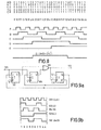
- Fig. 6a illustrates the case bo with flipflops (JK) 22, 24, 26 input terminal 20, and an output decoder which comprises OR-gate 28 and an AND-gate 30 in order to produce the output signal on output terminal 32.
- Fig. 6b illustrates the case dl with flipflops 36, 38, 40, input terminal 34 and an output decoder with an OR-gate 42, and an AND-gate 44 in order to produce the output signal on output terminal 46.
- the OR-gate 42 is also used for producing an input signal for the flipflop 36.
- the "values" of the flipflops are again indicated.
- the function to be formed by an output decoder is stated (the prime each time denotes the inverted value of a quantity).
- the symmetry of the output signal is then better than for a divider by 2t: the two intervals 1 and 0 relate as 3:4.
- Fig. 8 shows a half cycle of a counter with five bistable elements which thus have the values 16, 1, 2, 4 and 8.
- the figure shows 31 states successively reached in a change-by-one code.
- the second half of the cycle is completed in the opposite direction.
- the last line but one shows the function to be formed by an output decoder.
- the last line shows the output signal.
- the lengths of the "1" and "0" periods relate as 15:16.
- the first cycle half is terminated after 23 states.
- the output decoder must then also be adapted.
- a further method of forming a cycle for a low divisor from a cycle for a large divisor is as follows.
- a pair of successive, equal states is omitted from a cycle, said pair being surrounded by mutually equal states.
- the pair of states 11 or 22 (or both) can be omitted from the cycle AJ.
- two equal successive states can be omitted if they are surrounded by mutually unequal states.
- the states 55 or 66 (or both) can be omitted from the cycle FO in Fig. 2.
- a change-by-one code cycle can then change-over into a change-by-more-than-one code cycle.
- Standard elements can be used for the JK flipflops.
- the tables do not take into account the fact that a JK flipflop which reacts to a positive-going edge is usually constructed as a so-termed JK flipflop.
- flipflops examples include the circuit Signer tics 54109, comprising two "positive edge” JK flipflops, and Signetics 54112 comprising two "negative edge” JK flipflops.
- Fig. 9a shows a divider by 2 which operates according to a partly asynchronous principle.
- the divider comprises an input 100 for a clock signal, three flipflops 102, 104, 106, a logic OR-gate 108 with two inputs, and an output terminal 110.
- the flipflop 102 reacts to the positiv- going clock pulse edges.
- the flipflop 104 reacts to the negative-going clock pulse edges.
- the flipflop 106 reacts each time to the positive-going edges of the output signal of the OR-gate 108.
- the flipflops 102, 106 are constructed as JK flipflops and the flipflop 104 is constructed as a JK flipflop.
- Fig. 9b shows a cycle of ten states of the divider by 2 in accordance with Fig 9a. All counter states are mutually unequal again after a positive-going clock pulse edge. The same is applicable to all counter states directly after a negative-going clock pulse edge. Furthermore, two pairs of two directly successive, identical states occur.
- Fig. 9c shows a logic tree structure of states which can be obtained by means of three flipflops, starting arbitrarily at the state "O".
- the left column shows the numbering of the ten states and the direction of the clock pulse edges. For example, from state 0 state 6 and state 2 be reached in reaction to a negative-going edge. The latter possibility appaars to be (Fig. 9b) the reversal of the cycle and this possibility will not be separately considered.
- the states 6 and 7 can be reached from the state 6.
- the figure subsequently shows all possibilities leading to a cycle of ten states.
- the last curve in Fig, 9b represents the output signal, i.e. of the possibility III.
- Fig. 9d shows the input signals (JA, KA, JB, KB, CKC) required for the A, B, C flipflops and the function (U) to be formed by an output decoder for a symmetrical output signal.
- the last column indicates the number of logic gates required for the output decoder and for activating the flipflops.
- n flipflops for example n-4
- a complete change-by-one code in accordance with Gray for n-1 flipflops is: 04513762, which is the "first group" of states.
- a second, subsequent group of states is formed by the first group in the reverse order.
- a next group of states is formed by the second group minus the state "O”.
- a fourth, subsequent group of states is formed by the first group minus the state "O".
- the last (D) flipflop (JK type) is in the "1" state and in the "0" state again for 15 successive states.
- the foregoing thus results in a divider by 7 , the output signal again being equal to the activation signal of the last flipflop.
- the divisor can be reduced again.
- the control of the various stages will not be elaborated for the sake of brevity, because it has already been done for the divider by 2 in Fig. 9d.
Landscapes
- Stabilization Of Oscillater, Synchronisation, Frequency Synthesizers (AREA)
- Synchronizing For Television (AREA)
- Synchronisation In Digital Transmission Systems (AREA)
- Television Systems (AREA)
Applications Claiming Priority (2)
| Application Number | Priority Date | Filing Date | Title |
|---|---|---|---|
| NL7902111A NL7902111A (nl) | 1979-03-16 | 1979-03-16 | Inrichting voor het delen van een terugkerend ingangs- signaal door een gebroken faktor f, met name voor f=n-1/2. |
| NL7902111 | 1979-03-16 |
Publications (2)
| Publication Number | Publication Date |
|---|---|
| EP0017268A1 true EP0017268A1 (de) | 1980-10-15 |
| EP0017268B1 EP0017268B1 (de) | 1982-11-03 |
Family
ID=19832823
Family Applications (1)
| Application Number | Title | Priority Date | Filing Date |
|---|---|---|---|
| EP80200164A Expired EP0017268B1 (de) | 1979-03-16 | 1980-02-27 | Anordnung zum Teilen eines sich wiederholenden Eingangssignals durch einen nicht ganzzahligen Teiler f, insbesondere f=N-1/2 und ihre Verwendung in einer Fernsehbildanzeige |
Country Status (12)
| Country | Link |
|---|---|
| US (1) | US4354188A (de) |
| EP (1) | EP0017268B1 (de) |
| JP (1) | JPS55127734A (de) |
| AU (1) | AU531205B2 (de) |
| CA (1) | CA1139887A (de) |
| DE (1) | DE3061017D1 (de) |
| ES (1) | ES489547A1 (de) |
| FI (1) | FI69229C (de) |
| HK (1) | HK30183A (de) |
| NL (1) | NL7902111A (de) |
| NZ (1) | NZ193118A (de) |
| SG (1) | SG13683G (de) |
Cited By (2)
| Publication number | Priority date | Publication date | Assignee | Title |
|---|---|---|---|---|
| EP0473251A1 (de) * | 1990-08-24 | 1992-03-04 | Mitsubishi Denki Kabushiki Kaisha | Frequenzteiler und Impulsformer |
| DE202012011916U1 (de) | 2012-12-13 | 2013-02-18 | Heinz Polak | Lawinen- und Tiefschneeband |
Families Citing this family (8)
| Publication number | Priority date | Publication date | Assignee | Title |
|---|---|---|---|---|
| JPS59181831A (ja) * | 1983-03-31 | 1984-10-16 | Toshiba Corp | 可変分周器 |
| US4587664A (en) * | 1983-09-21 | 1986-05-06 | Nec Corporation | High speed frequency divider dividing pulse by a number obtained by dividing an odd number by two |
| SE445868B (sv) * | 1984-12-12 | 1986-07-21 | Ellemtel Utvecklings Ab | Anordning for neddelning av en klockfrekvens |
| JPS623229A (ja) * | 1985-06-28 | 1987-01-09 | Sharp Corp | 液晶駆動方式 |
| JPH09114443A (ja) | 1995-10-20 | 1997-05-02 | Seiko Epson Corp | 映像スケーリング装置 |
| US6707326B1 (en) * | 1999-08-06 | 2004-03-16 | Skyworks Solutions, Inc. | Programmable frequency divider |
| US7227920B2 (en) * | 2001-06-26 | 2007-06-05 | Nokia Corporation | Circuit and method for correcting clock duty cycle |
| US6882229B1 (en) | 2003-07-23 | 2005-04-19 | Pericom Semiconductor Corp. | Divide-by-X.5 circuit with frequency doubler and differential oscillator |
Citations (3)
| Publication number | Priority date | Publication date | Assignee | Title |
|---|---|---|---|---|
| US3189832A (en) * | 1962-09-18 | 1965-06-15 | Bell Telephone Labor Inc | Pulse train repetition rate divider that divides by n+1/2 where n is a whole number |
| US3943379A (en) * | 1974-10-29 | 1976-03-09 | Rca Corporation | Symmetrical odd modulus frequency divider |
| US4041403A (en) * | 1975-07-28 | 1977-08-09 | Bell Telephone Laboratories, Incorporated | Divide-by-N/2 frequency division arrangement |
Family Cites Families (3)
| Publication number | Priority date | Publication date | Assignee | Title |
|---|---|---|---|---|
| US3446947A (en) * | 1965-11-30 | 1969-05-27 | Bell Telephone Labor Inc | Pulse train repetition rate divider that divides by a fractional number |
| JPS5017958A (de) * | 1973-06-19 | 1975-02-25 | ||
| US3906374A (en) * | 1974-03-12 | 1975-09-16 | Nasa | Symmetrical odd-modulus frequency divider |
-
1979
- 1979-03-16 NL NL7902111A patent/NL7902111A/nl not_active Application Discontinuation
-
1980
- 1980-02-27 DE DE8080200164T patent/DE3061017D1/de not_active Expired
- 1980-02-27 EP EP80200164A patent/EP0017268B1/de not_active Expired
- 1980-03-06 CA CA000347106A patent/CA1139887A/en not_active Expired
- 1980-03-13 FI FI800778A patent/FI69229C/fi not_active IP Right Cessation
- 1980-03-14 US US06/130,285 patent/US4354188A/en not_active Expired - Lifetime
- 1980-03-14 AU AU56442/80A patent/AU531205B2/en not_active Ceased
- 1980-03-14 ES ES489547A patent/ES489547A1/es not_active Expired
- 1980-03-17 JP JP3466580A patent/JPS55127734A/ja active Granted
- 1980-05-13 NZ NZ193118A patent/NZ193118A/xx unknown
-
1983
- 1983-03-24 SG SG136/83A patent/SG13683G/en unknown
- 1983-08-25 HK HK301/83A patent/HK30183A/xx unknown
Patent Citations (3)
| Publication number | Priority date | Publication date | Assignee | Title |
|---|---|---|---|---|
| US3189832A (en) * | 1962-09-18 | 1965-06-15 | Bell Telephone Labor Inc | Pulse train repetition rate divider that divides by n+1/2 where n is a whole number |
| US3943379A (en) * | 1974-10-29 | 1976-03-09 | Rca Corporation | Symmetrical odd modulus frequency divider |
| US4041403A (en) * | 1975-07-28 | 1977-08-09 | Bell Telephone Laboratories, Incorporated | Divide-by-N/2 frequency division arrangement |
Non-Patent Citations (1)
| Title |
|---|
| IBM TECHNICAL DISCLOSURE BULLETIN, Vol. 17, No. 12, May 1975, pages 3619-3620 New York, U.S.A. C. KARABATSOS et al.: "Synchronous Frequency Division by 2.5" * Figure; pages 3619-3620 * * |
Cited By (3)
| Publication number | Priority date | Publication date | Assignee | Title |
|---|---|---|---|---|
| EP0473251A1 (de) * | 1990-08-24 | 1992-03-04 | Mitsubishi Denki Kabushiki Kaisha | Frequenzteiler und Impulsformer |
| US5172400A (en) * | 1990-08-24 | 1992-12-15 | Mitsubishi Denki Kabushiki Kaisha | Frequency divider employing multiple stages of master/slave flip-flops |
| DE202012011916U1 (de) | 2012-12-13 | 2013-02-18 | Heinz Polak | Lawinen- und Tiefschneeband |
Also Published As
| Publication number | Publication date |
|---|---|
| JPS55127734A (en) | 1980-10-02 |
| DE3061017D1 (en) | 1982-12-09 |
| CA1139887A (en) | 1983-01-18 |
| FI69229B (fi) | 1985-08-30 |
| EP0017268B1 (de) | 1982-11-03 |
| FI69229C (fi) | 1985-12-10 |
| ES489547A1 (es) | 1980-09-16 |
| SG13683G (en) | 1983-09-16 |
| NL7902111A (nl) | 1980-09-18 |
| US4354188A (en) | 1982-10-12 |
| FI800778A7 (fi) | 1980-09-17 |
| NZ193118A (en) | 1982-11-23 |
| AU531205B2 (en) | 1983-08-11 |
| AU5644280A (en) | 1980-09-18 |
| JPH0255975B2 (de) | 1990-11-28 |
| HK30183A (en) | 1983-09-02 |
Similar Documents
| Publication | Publication Date | Title |
|---|---|---|
| EP0107236A1 (de) | Mehrfachredundantes Taktsystem eine Anzahl von gegenseitig synchronisierenden Takten enthaltend, und Taktschaltung zum Gebrauch in einem solchen Taktsystem | |
| US3742197A (en) | Synthesis of digital signals corresponding to selected analog signals | |
| EP0017268B1 (de) | Anordnung zum Teilen eines sich wiederholenden Eingangssignals durch einen nicht ganzzahligen Teiler f, insbesondere f=N-1/2 und ihre Verwendung in einer Fernsehbildanzeige | |
| EP0076082B1 (de) | Anzeigedatenverarbeitungsgerät | |
| JPH05284362A (ja) | ジグザグアドレスの発生方法及びその発生回路 | |
| US3648250A (en) | Digital video display system using cathode-ray tube | |
| US5189685A (en) | Fast counter/divider and its use in a swallower counter | |
| US5396236A (en) | Converting method of vertical data/horizontal data and a circuit therefor | |
| US4477918A (en) | Multiple synchronous counters with ripple read | |
| US4425562A (en) | Device for coding signals which are distributed between a number of channels | |
| EP0548649A2 (de) | Parallel DS3 AIS/Ruhe Kodegenerator | |
| US4696020A (en) | Digital circuit for frequency or pulse rate division | |
| US3920901A (en) | Generator used for time synchronization in video-telephone | |
| US5990811A (en) | Transfer clock converter for digital data | |
| US4023145A (en) | Time division multiplex signal processor | |
| JPH0748824B2 (ja) | 固体撮像素子用クロツク発生器 | |
| US4152698A (en) | Digital-to-analog converter with scanning system | |
| KR100306235B1 (ko) | 고주파를카운트하기위한카운터 | |
| KR200155054Y1 (ko) | 카운터 회로 | |
| JP2547723B2 (ja) | 分周回路 | |
| KR920006931Y1 (ko) | 홀수분주회로 | |
| SU1247862A1 (ru) | Устройство дл делени чисел | |
| SU1424127A1 (ru) | Устройство дл определени потери достоверности дискретной информации | |
| US3700808A (en) | Distortion analysis system and method | |
| SU942104A1 (ru) | Устройство дл опроса каналов телеметрической системы |
Legal Events
| Date | Code | Title | Description |
|---|---|---|---|
| PUAI | Public reference made under article 153(3) epc to a published international application that has entered the european phase |
Free format text: ORIGINAL CODE: 0009012 |
|
| AK | Designated contracting states |
Designated state(s): BE DE FR GB IT NL |
|
| 17P | Request for examination filed | ||
| ITF | It: translation for a ep patent filed | ||
| GRAA | (expected) grant |
Free format text: ORIGINAL CODE: 0009210 |
|
| AK | Designated contracting states |
Designated state(s): BE DE FR GB IT NL |
|
| REF | Corresponds to: |
Ref document number: 3061017 Country of ref document: DE Date of ref document: 19821209 |
|
| ET | Fr: translation filed | ||
| PGFP | Annual fee paid to national office [announced via postgrant information from national office to epo] |
Ref country code: GB Payment date: 19900131 Year of fee payment: 11 |
|
| PGFP | Annual fee paid to national office [announced via postgrant information from national office to epo] |
Ref country code: BE Payment date: 19900207 Year of fee payment: 11 |
|
| PGFP | Annual fee paid to national office [announced via postgrant information from national office to epo] |
Ref country code: FR Payment date: 19900220 Year of fee payment: 11 |
|
| ITTA | It: last paid annual fee | ||
| PGFP | Annual fee paid to national office [announced via postgrant information from national office to epo] |
Ref country code: NL Payment date: 19900228 Year of fee payment: 11 |
|
| PGFP | Annual fee paid to national office [announced via postgrant information from national office to epo] |
Ref country code: DE Payment date: 19900424 Year of fee payment: 11 |
|
| PG25 | Lapsed in a contracting state [announced via postgrant information from national office to epo] |
Ref country code: GB Effective date: 19910227 |
|
| PG25 | Lapsed in a contracting state [announced via postgrant information from national office to epo] |
Ref country code: BE Effective date: 19910228 |
|
| PG25 | Lapsed in a contracting state [announced via postgrant information from national office to epo] |
Ref country code: NL Effective date: 19910901 |
|
| NLV4 | Nl: lapsed or anulled due to non-payment of the annual fee | ||
| GBPC | Gb: european patent ceased through non-payment of renewal fee | ||
| PG25 | Lapsed in a contracting state [announced via postgrant information from national office to epo] |
Ref country code: FR Effective date: 19911031 |
|
| PG25 | Lapsed in a contracting state [announced via postgrant information from national office to epo] |
Ref country code: DE Effective date: 19911101 |
|
| REG | Reference to a national code |
Ref country code: FR Ref legal event code: ST |
|
| PLBE | No opposition filed within time limit |
Free format text: ORIGINAL CODE: 0009261 |
|
| STAA | Information on the status of an ep patent application or granted ep patent |
Free format text: STATUS: NO OPPOSITION FILED WITHIN TIME LIMIT |