EP0020787A1 - Unite a semi-conducteur de haute frequence - Google Patents
Unite a semi-conducteur de haute frequence Download PDFInfo
- Publication number
- EP0020787A1 EP0020787A1 EP80900085A EP80900085A EP0020787A1 EP 0020787 A1 EP0020787 A1 EP 0020787A1 EP 80900085 A EP80900085 A EP 80900085A EP 80900085 A EP80900085 A EP 80900085A EP 0020787 A1 EP0020787 A1 EP 0020787A1
- Authority
- EP
- European Patent Office
- Prior art keywords
- high frequency
- circuit
- substrate
- frequency semiconductor
- semiconductor device
- Prior art date
- Legal status (The legal status is an assumption and is not a legal conclusion. Google has not performed a legal analysis and makes no representation as to the accuracy of the status listed.)
- Granted
Links
Images



Classifications
-
- H—ELECTRICITY
- H10—SEMICONDUCTOR DEVICES; ELECTRIC SOLID-STATE DEVICES NOT OTHERWISE PROVIDED FOR
- H10W—GENERIC PACKAGES, INTERCONNECTIONS, CONNECTORS OR OTHER CONSTRUCTIONAL DETAILS OF DEVICES COVERED BY CLASS H10
- H10W44/00—Electrical arrangements for controlling or matching impedance
- H10W44/20—Electrical arrangements for controlling or matching impedance at high-frequency [HF] or radio frequency [RF]
-
- H—ELECTRICITY
- H10—SEMICONDUCTOR DEVICES; ELECTRIC SOLID-STATE DEVICES NOT OTHERWISE PROVIDED FOR
- H10W—GENERIC PACKAGES, INTERCONNECTIONS, CONNECTORS OR OTHER CONSTRUCTIONAL DETAILS OF DEVICES COVERED BY CLASS H10
- H10W76/00—Containers; Fillings or auxiliary members therefor; Seals
- H10W76/10—Containers or parts thereof
- H10W76/12—Containers or parts thereof characterised by their shape
- H10W76/13—Containers comprising a conductive base serving as an interconnection
- H10W76/134—Containers comprising a conductive base serving as an interconnection having other interconnections parallel to the conductive base
-
- H—ELECTRICITY
- H10—SEMICONDUCTOR DEVICES; ELECTRIC SOLID-STATE DEVICES NOT OTHERWISE PROVIDED FOR
- H10W—GENERIC PACKAGES, INTERCONNECTIONS, CONNECTORS OR OTHER CONSTRUCTIONAL DETAILS OF DEVICES COVERED BY CLASS H10
- H10W76/00—Containers; Fillings or auxiliary members therefor; Seals
- H10W76/10—Containers or parts thereof
- H10W76/12—Containers or parts thereof characterised by their shape
- H10W76/15—Containers comprising an insulating or insulated base
- H10W76/157—Containers comprising an insulating or insulated base having interconnections parallel to the insulating or insulated base
-
- H—ELECTRICITY
- H10—SEMICONDUCTOR DEVICES; ELECTRIC SOLID-STATE DEVICES NOT OTHERWISE PROVIDED FOR
- H10W—GENERIC PACKAGES, INTERCONNECTIONS, CONNECTORS OR OTHER CONSTRUCTIONAL DETAILS OF DEVICES COVERED BY CLASS H10
- H10W90/00—Package configurations
-
- H—ELECTRICITY
- H10—SEMICONDUCTOR DEVICES; ELECTRIC SOLID-STATE DEVICES NOT OTHERWISE PROVIDED FOR
- H10W—GENERIC PACKAGES, INTERCONNECTIONS, CONNECTORS OR OTHER CONSTRUCTIONAL DETAILS OF DEVICES COVERED BY CLASS H10
- H10W90/00—Package configurations
- H10W90/701—Package configurations characterised by the relative positions of pads or connectors relative to package parts
- H10W90/731—Package configurations characterised by the relative positions of pads or connectors relative to package parts of die-attach connectors
- H10W90/737—Package configurations characterised by the relative positions of pads or connectors relative to package parts of die-attach connectors between a chip and a laterally-adjacent lead frame, conducting package substrate or heat sink
Definitions
- This invention relates to a high frequency semiconductor device, and more particularly, to a structure of the high frequency semiconductor device which provides a circuit substrate for mounting active elements such as transistors, passive elements such as capacitors and resistors and a package for accommodating said substrate and handles a high frequency signal such as microwave signal.
- a high frequency semiconductor device for example, a microwave amplifier provides a circuit substrate for mounting active element such as transistors, passive element such as capacitors, resistors and inductors and a package for accommodating them.
- a transistor which is hermetically sealed for preventing degradation of characteristic and has leads for connection with other circuit elements is mounted on a circuit substrate, it is connected with the other elements which are also mounted on the same circuit substrate and are required for forming an amplifier via circuits formed on said substrate, then such circuit substrate has been housed in a metal case.
- a transistor for example, among various elements forming an amplifier is hermetically sealed and resultingly it occupies large space, requiring a large size of circuit substrate in order to mount it and resultant size of case.
- transistor chips are mounted together with other necessary circuit elements on the circuit substrate provided on the metal base without individual hermetical sealing and then such circuit substrate is accommodated in a metal case and .then this metal case is hermetically sealed.
- a metal case has an advantage that physical dimensions are reduced as compared with said existing structure but at the same time has following disadvantage that perfect sealing becomes difficult because sealing is required for longer distance when considering it from the point of view of hermetically sealing elements.
- An object of the present invention lies in offering a high frequency semiconductor device which is designed compact as a whole even being connected in multi-stage, moreover with sufficient hermetical sealing.
- Another object of the present invention lies in offering a high frequency semiconductor device having such a configuration that plurality of high frequency semiconductor devices respectively having a function as an amplifier are directly cascade-connected without intervention of any elements in case of forming, for example, a multi-stage amplfier circuit.
- a high frequency semiconductor device which is designed small in size with sufficient sealing and can easily be used for assembling system by providing; a metal base substrate on which a function device having at least one semiconductor element, a DC circuit for operating said semiconductor element and a high frequency circuit for cascade-connecting said semiconductor element function with an external circuit are mounted and is used as the ground electrode for a high frequency component; insulating substrate which surrounds said function device in the form of a frame and simultaneously provides a plurality of independent metallized part for the connection with the external circuits at it surface; and the sealing part for hermetically sealing said function device.
- Figure 1 is a perspective view of the uncovered outline of a high frequency semiconductor device of the present invention.
- Figure 2 shows a metal base substrate 1.
- Figure 2A is a plan view, while Figure 2B is a cross-section of Fig. 2A along the line A-A'.
- Figure 3 shows a structure in which an insulating substrate 3 is mounted on the metal base substrate 1.
- Figure 3A is a plan view, while Figure 3B is a cross-section along the line A-A' of Fig. 3A.
- Figure 4 shows a structure in which an insulating frame 8 is mounted on the insulating substrate 3 and a circuit substrate 4 is disposed on a support 21 of the metal base substrate.
- Figure 4A is a plan view, while Figure 4B is a cross-section along the line A-A' of Figure 4A.
- Figure 5 shows a structure in which a cover 51 is mounted on the insulating frame 8.
- Figure 5A is a plan view, while Figure 5B is a cross-section along the line .A-A' of Figure 5A.
- Figure 6 shows a high frequency semiconductor device of the present invention, particularly an amplifier circuit of microwave signal amplifier.
- Figure 7 shows a functional block diagram of the circuit shown in Fig. 6.
- Figure 8 shows an equivalent circuit of the ampli- . fier shown in Fig. 7.
- Figure 9 shows a structure in which the microwave amplifier of three-stage by the present invention is housed in a case.
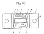
- Figure 10 is a plan view of another embodiment of the present invention.
- FIG. 1 shows a perspective view of outline of a high frequency semiconductor device of the present invention, from which a cover for hermetical sealing is now removed.
- This high frequency semiconductor device is for instance, a microwave amplifier.
- the insulating substrate 3 consisting of insulating material such as ceramic is provided on the metal base substrate 1 which is composed of no acidic copper element and has mounting screw holes 2, this insulating substrate 3 is provided with hole part at its center, and herein the circuit substrate 4 on which various elements are mounted to form a microwave amplifier circuits such as transistors and the matching circuit consisting of capacitors and inductors and directional couplers is.built in.
- the metallized layers 5,6,7, 7', for connecting between a microwave amplifier formed on the circuit substrate 4 and external circuits, are formed on the insulating substrate 3.
- the metallized layer 5 is, for example, the one for high frequency signal input of a microwave amplifier circuit and is extended up to the outer end of the insulating substrate 3 from the hole part of insulating substrate 3 as in the case of the metallized layer 6.
- a metallized layer for a high frequency signal output is formed at the areas of the insulating substrate 3 facing each other and sandwiching the circuit substrate 4.
- the metallized layer 6 is the one for supplying DC voltage, and its end has the same shape as the metallized layers 7 or 7'..
- the ends of the metalized layers 7, 7' are disposed face to face each other, and the one electrode is connected to the other electrode of the grounded capacitor (not illustrated)respectively via a wire and a resistor.
- These metallized layers are formed by the following processes that the tungsten paste is coated by the screen printing method and baked, and thereafter nickel plating or gold plating is performed.
- the insulating frame 8 consisting of ceramic material is provided crossing these metallize layer, and moreover a cover (not illustrated) for sealing is placed and the sealing part is formed thereupon.
- the lead 9 may be provided as indicated in the figure in accordance with a method of using a high frequency semiconductor device.
- Figure 1 shows a structure in which a lead is not provided at a point.of the metallized layer 6 for the convenience of explanation.
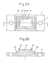
- Figure 2 shows the metal base substrate 1.
- Figure 2A is a plan view, while Fig. 2B is a cross-section along the line A-A' of Fig. 2A.
- the metal base substrate 1 is provided with the base 21 on which the circuit substrate is mounted and the projections 22, 22', 22" for grounding peneral parts of the circuit on the circuit substrate.
- the support 23 for supporting the insulating substrate is provided.
- Figure 3 shows the condition where the insulating substrate 3 is mounted on the metal base substrate 1.
- Figure 3A is a plan view, while Figure 3B is a cross-section along the line A-A' of Fig. 3A.
- the insulating substrate 3 is supported by the circumference of base 21 and the support 23.
- the metal base substrate 1 and insulating substrate 3 are bonded with the silver solder.
- the insulating substrate 3 is provided with the hole portion 31 for accommodating the circuit substrate, and said hole part 31 is provided with a dent groove 32 so that the plating solution does not remain in the gap between the base 21 and support 23 and flows out therefrom when golt plating is performed on the metal.base substrate 1 under the condition that the insulating substrate 3 is mounted.
- the metallized layer 5 for a high frequency signal and the metallized layer 6 for supplying a DC bias to the microwave amplifier circuit are formed.
- Figure 4 shows the conditions where the insulating frame 8 is mounted on the insulating substrate 3 and the circuit substrate 4 is mounted on the base of metal base substrate.
- Figure 4A is a plan view, while Figure 4B is a cross-section along the line A-A' of Fig. 4A.
- the insulating substrate 3 and insulating frame 8 are bonded with the alumina.
- the metallized layer 5 for a high frequency signal is connected with the input and output ends of a directional coupler (not illustrated) via the wire etc. at the inside of the insulating frame 8.
- the metallized layer 6 for DC power supply is connected to an element formed on the circuit substrate 4 via the wire etc. at the ends 7, 7' at the inside of the insulating frame 8.
- various elements formed on the circuit substrate 4 are not illustrated since these will be explained later in detail.
- Figure 5 shows a structure in which a cover 51 is mounted on the insulating frame 8.
- Figure 5A is a plan view, while Figure 5B a cross-section along the line A-A' of Fig. 5A.
- the cover 51 is made of an insulator such as ceramic or a metal element such as covar, and is bonded to the insulating frame 8 with an alloy AuSn (20) of the gold (Au) and tin (Sn).
- the insulating frame 8 and cover 51 form the sealing part of a high frequency semiconductor device of the present invention, but as a sealing part, a metal, for example, a covar can be used in the form of integrating the insulating frame and cover.
- a metal for example, a covar
- coupling between both metallized layers can be prevented by providing a metallized layer, which reaches the metal base substrate, between the metallized layers for a high frequency signal and DC signal.
- a microwave amplifier circuit formed on the circuit substrate will be explained.
- FIG. 6 shows a high frequency semiconductor device of the present invention, particularly an amplification circuit of a microwave amplifier.
- the amplifier circuit formed on the circuit substrate 4 is a balance type amplifier circuit, showing nearly symmetrical characteristics in the right and left sides.
- a microwave input signal being input to the input terminal IN of the directional (hybrid) coupler HC 1 is divided into a couple of signals therein and these divided signals are respectively amplified by the amplifiers 71 and 72, and then combined by the hybrid coupler HC 2.
- an amplified microwave signal is output from the output terminal OUT.
- each one end of the hybrid couplers HC 1 and HC 2 is respectively terminated by the resistors R s1 and R s2 .
- Ca, Cb, Cc and Cd denote DC block capacitors.
- the amplifiers 71 and 72 have the similar structure and for example, a concrete equivalent circuit of the amplifier 71 is shown in Fig. 8.
- 81 is the input end of amplifier 71 and the input matching circuit is composed of inductors L 2 , L 3 and capacitor C 2 , while the output matching circuit is formed by inductors L4, L 5 and capacitor C4; the gate self- bias circuit by inductor L l , resistors R 1 and R 2 , capacitor C 3 ; and the drain bias circuit by inductor L6, resistor R 3 and capacitor C 5 .
- Figure 6 shows an enlarged view of the circuit substrate 4 on which an amplifier circuit is formed and the area near to the hole part of the insulating substrate 3.
- the input end IN of the hybrid coupler HC 1 and the output end OUT of the hybrid coupler HC 2 are respectively connected with the metallized layer 5, formed on the insulating substrate, for a high frequency signal, and the one electrodes of the grounded elements, for example, termination resistors R sl , R s2 and capacitors C 2 , C 4 , are.connected to the projections 22, 22', 22" of the metal base substrate.
- the edges 7, 7' of metallized layer for DC power supply are connected to a resistor R 4 by wire and the resistor R 4 is connected to the upper electrode of a capacitor C 6 and its lower electrode is connected to the metal base substrate for grounding as shown in Fig. 6.
- the wire is bridged between the resistor R 4 and the input end 83 of the bias circuit and thereby a bias voltage is supplied from an external circuit to the resistor R 3 forming a bias circuit. It is also possible to directly connect the metallized layers 7 and 7' by wire in order to supply the externally supplied bias voltage to the metallized layer 7' from layer 7, but resonance sometimes occurs between the facing metallized layers 7 and 7' and therefore grounding is made through the resistor R4 and capacitor C6 in order to prevent such resonance. A part of various elements of these circuit may be obtained as the monolithic elements.
- amplification element such as a field effect transistor
- circuits which perform a perfect function accompanied with the amplification element as the amplification circuit, such as input/output matching circuit and directional coupler etc. are housed in a single case.
- a high frequency semiconductor device itself has the perfect function as the amplifier without connection with any external matching circuit etc. Therefore, in case of using this device as an amplifier of single stage, a single amplifier can be obtained by providing leads to the metalized layers and an amplifier of multi-stage can also be formed by the connection as shown in Fig. 9.
- Figure 9 shows a configuration of the microwave . amplifier of three stages.
- the microwave amplifiers 91, 92, 93 are fixed to a metal case 94 by screwing through side-by-side arrangement of each metal base substrate 1, the metallized layers for DC and high frequency are arranged face to face respectively.
- the microwave signal input from the input connector 98 of the metal case is amplified by amplifiers 91, 92, 93 of three stages and then output from the output connector 99 by connecting above mentioned metallized layers with wire or conductive ribbon, the high frequency metallized layer 5 of the microwave amplifier 91 to the strip line 95, the DC metallized layer 6 to the bias terminal 96 provided in the metal case 94 respectively and simultaneously the high frequency metallized layer 5 of . the microwave amplifier 93 to the strip line 97.
- a bias voltage which is required for the function of amplifier is respectively supplied to the amplifiers 91, 92 and 93 only by connecting the bias power supply to the bias terminal 96.
- the metal case 94 requires a cover but it doesn't require to be hermetically sealed because each amplifier is already hermetically sealed.
- a high frequency semiconductor device of the present invention has a completed function. Therefore, in case of forming a system by using these devices, there is no need of connecting the matching circuit as an external circuit and a system can be formed with a concept of the block diagram in the stage of system design. For this reason, system assembling can be made very easily.
- Figure 10 shows another embodiment of the present invention indicating a structure in which an insulating frame is not installed, just like the one in Fig. 3. However, the circuit substrate 4' is housed in the hole part of the insulating substrate 3.
- the hybrid couplers HCl, HC2 which are mounted on the circuit substrate in the first embodiment are provided on the insulating substrate 3.
- the hybrid coupler used particularly in the balance type amplifier circuit of a high frequency semiconductor device cannot be reduced in size since the coupling part requires a length of 1/4 of the wavelength of signal used inspite the other elements can be reduced in size, occupying a greater part of the circuit substrate.
- the present invention is capable of offering a high frequency semiconductor device which is small in size, provides sufficient sealing and ensured easy system assembling.
Landscapes
- Microwave Amplifiers (AREA)
- Semiconductor Integrated Circuits (AREA)
Abstract
Applications Claiming Priority (4)
| Application Number | Priority Date | Filing Date | Title |
|---|---|---|---|
| JP16316778A JPS5587460A (en) | 1978-12-26 | 1978-12-26 | Package |
| JP163167/78 | 1978-12-26 | ||
| JP53164786A JPS596513B2 (ja) | 1978-12-28 | 1978-12-28 | マイクロ波装置モジユ−ル |
| JP164786/78 | 1978-12-28 |
Publications (3)
| Publication Number | Publication Date |
|---|---|
| EP0020787A1 true EP0020787A1 (fr) | 1981-01-07 |
| EP0020787A4 EP0020787A4 (fr) | 1981-05-15 |
| EP0020787B1 EP0020787B1 (fr) | 1983-08-03 |
Family
ID=26488700
Family Applications (1)
| Application Number | Title | Priority Date | Filing Date |
|---|---|---|---|
| EP80900085A Expired EP0020787B1 (fr) | 1978-12-26 | 1980-07-14 | Unite a semi-conducteur de haute frequence |
Country Status (3)
| Country | Link |
|---|---|
| EP (1) | EP0020787B1 (fr) |
| DE (1) | DE2966040D1 (fr) |
| WO (1) | WO1980001437A1 (fr) |
Cited By (1)
| Publication number | Priority date | Publication date | Assignee | Title |
|---|---|---|---|---|
| JP2017174872A (ja) * | 2016-03-22 | 2017-09-28 | 京セラ株式会社 | 半導体素子収納用パッケージおよび半導体装置 |
Family Cites Families (5)
| Publication number | Priority date | Publication date | Assignee | Title |
|---|---|---|---|---|
| JPS5137512Y1 (fr) * | 1969-03-26 | 1976-09-14 | ||
| US3626259A (en) * | 1970-07-15 | 1971-12-07 | Trw Inc | High-frequency semiconductor package |
| US3740672A (en) * | 1971-11-22 | 1973-06-19 | Rca Corp | Semiconductor carrier for microwave applications |
| US3886505A (en) * | 1974-04-29 | 1975-05-27 | Rca Corp | Semiconductor package having means to tune out output capacitance |
| JPS53136961A (en) * | 1977-05-04 | 1978-11-29 | Nec Corp | Internal-matched high frequency semiconductor device |
-
1979
- 1979-12-22 WO PCT/JP1979/000323 patent/WO1980001437A1/fr not_active Ceased
- 1979-12-22 DE DE8080900085T patent/DE2966040D1/de not_active Expired
-
1980
- 1980-07-14 EP EP80900085A patent/EP0020787B1/fr not_active Expired
Cited By (1)
| Publication number | Priority date | Publication date | Assignee | Title |
|---|---|---|---|---|
| JP2017174872A (ja) * | 2016-03-22 | 2017-09-28 | 京セラ株式会社 | 半導体素子収納用パッケージおよび半導体装置 |
Also Published As
| Publication number | Publication date |
|---|---|
| EP0020787B1 (fr) | 1983-08-03 |
| WO1980001437A1 (fr) | 1980-07-10 |
| EP0020787A4 (fr) | 1981-05-15 |
| DE2966040D1 (en) | 1983-09-08 |
Similar Documents
| Publication | Publication Date | Title |
|---|---|---|
| US4427991A (en) | High frequency semiconductor device | |
| US4908694A (en) | Semiconductor device | |
| US4126840A (en) | Filter connector | |
| JPS61208902A (ja) | Mic型誘電体フイルタ | |
| EP0117434A1 (fr) | Sous-système hybride à micro-ondes | |
| JP2609634B2 (ja) | チップ化モジュール | |
| US6049126A (en) | Semiconductor package and amplifier employing the same | |
| JP3445811B2 (ja) | 高周波回路装置および無線機 | |
| EP0020787A1 (fr) | Unite a semi-conducteur de haute frequence | |
| JPH0210756A (ja) | マイクロウェーブ・チップの相互接続及び保護のためのデバイス | |
| CA1134489A (fr) | Semiconducteur haut frequence | |
| JP4206185B2 (ja) | 高周波半導体装置 | |
| JPH09260522A (ja) | 半導体装置 | |
| JPS6271301A (ja) | マイクロ波集積回路装置 | |
| JPH1093012A (ja) | 高周波集積回路装置 | |
| JP3301198B2 (ja) | 誘電体フィルタ | |
| JPH0272654A (ja) | Icパッケージ及びその接続構造 | |
| JPH0233963A (ja) | 高周波トランジスタ | |
| JPH0810745B2 (ja) | マイクロ波集積回路装置 | |
| JPH04129402A (ja) | マイクロ波回路用パッケージ | |
| JPH06244293A (ja) | Icチップ実装用パッケージ構造とその製造方法 | |
| JP2791301B2 (ja) | マイクロ波集積回路及びマイクロ波回路装置 | |
| JPH03123047A (ja) | マイクロ波集積回路 | |
| JPS61285738A (ja) | マイクロ波集積回路用外囲器とその接続方法 | |
| JPH06177500A (ja) | フレキシブル配線板 |
Legal Events
| Date | Code | Title | Description |
|---|---|---|---|
| PUAI | Public reference made under article 153(3) epc to a published international application that has entered the european phase |
Free format text: ORIGINAL CODE: 0009012 |
|
| 17P | Request for examination filed |
Effective date: 19800822 |
|
| AK | Designated contracting states |
Designated state(s): DE FR GB NL |
|
| GRAA | (expected) grant |
Free format text: ORIGINAL CODE: 0009210 |
|
| AK | Designated contracting states |
Designated state(s): DE FR GB NL |
|
| REF | Corresponds to: |
Ref document number: 2966040 Country of ref document: DE Date of ref document: 19830908 |
|
| ET | Fr: translation filed | ||
| PLBE | No opposition filed within time limit |
Free format text: ORIGINAL CODE: 0009261 |
|
| STAA | Information on the status of an ep patent application or granted ep patent |
Free format text: STATUS: NO OPPOSITION FILED WITHIN TIME LIMIT |
|
| 26N | No opposition filed | ||
| PGFP | Annual fee paid to national office [announced via postgrant information from national office to epo] |
Ref country code: FR Payment date: 19951212 Year of fee payment: 17 |
|
| PGFP | Annual fee paid to national office [announced via postgrant information from national office to epo] |
Ref country code: GB Payment date: 19951213 Year of fee payment: 17 |
|
| PGFP | Annual fee paid to national office [announced via postgrant information from national office to epo] |
Ref country code: DE Payment date: 19951222 Year of fee payment: 17 |
|
| PGFP | Annual fee paid to national office [announced via postgrant information from national office to epo] |
Ref country code: NL Payment date: 19951230 Year of fee payment: 17 |
|
| PG25 | Lapsed in a contracting state [announced via postgrant information from national office to epo] |
Ref country code: GB Effective date: 19961222 |
|
| PG25 | Lapsed in a contracting state [announced via postgrant information from national office to epo] |
Ref country code: NL Effective date: 19970701 |
|
| GBPC | Gb: european patent ceased through non-payment of renewal fee |
Effective date: 19961222 |
|
| PG25 | Lapsed in a contracting state [announced via postgrant information from national office to epo] |
Ref country code: FR Effective date: 19970829 |
|
| NLV4 | Nl: lapsed or anulled due to non-payment of the annual fee |
Effective date: 19970701 |
|
| PG25 | Lapsed in a contracting state [announced via postgrant information from national office to epo] |
Ref country code: DE Effective date: 19970902 |
|
| REG | Reference to a national code |
Ref country code: FR Ref legal event code: ST |