EP0021174A1 - Panneau de mémoire pour image de radiation - Google Patents
Panneau de mémoire pour image de radiation Download PDFInfo
- Publication number
- EP0021174A1 EP0021174A1 EP80103133A EP80103133A EP0021174A1 EP 0021174 A1 EP0021174 A1 EP 0021174A1 EP 80103133 A EP80103133 A EP 80103133A EP 80103133 A EP80103133 A EP 80103133A EP 0021174 A1 EP0021174 A1 EP 0021174A1
- Authority
- EP
- European Patent Office
- Prior art keywords
- panel
- radiation image
- colorant
- image storage
- colored
- Prior art date
- Legal status (The legal status is an assumption and is not a legal conclusion. Google has not performed a legal analysis and makes no representation as to the accuracy of the status listed.)
- Granted
Links
Images

Classifications
-
- G—PHYSICS
- G21—NUCLEAR PHYSICS; NUCLEAR ENGINEERING
- G21K—HANDLING OF PARTICLES OR IONISING RADIATION NOT OTHERWISE PROVIDED FOR; IRRADIATION DEVICES; GAMMA RAY OR X-RAY MICROSCOPES
- G21K4/00—Conversion screens for the conversion of the spatial distribution of X-rays or particle radiation into visible images, e.g. fluoroscopic screens
-
- F—MECHANICAL ENGINEERING; LIGHTING; HEATING; WEAPONS; BLASTING
- F21—LIGHTING
- F21K—NON-ELECTRIC LIGHT SOURCES USING LUMINESCENCE; LIGHT SOURCES USING ELECTROCHEMILUMINESCENCE; LIGHT SOURCES USING CHARGES OF COMBUSTIBLE MATERIAL; LIGHT SOURCES USING SEMICONDUCTOR DEVICES AS LIGHT-GENERATING ELEMENTS; LIGHT SOURCES NOT OTHERWISE PROVIDED FOR
- F21K2/00—Non-electric light sources using luminescence; Light sources using electrochemiluminescence
-
- G—PHYSICS
- G01—MEASURING; TESTING
- G01T—MEASUREMENT OF NUCLEAR OR X-RADIATION
- G01T1/00—Measuring X-radiation, gamma radiation, corpuscular radiation, or cosmic radiation
- G01T1/02—Dosimeters
- G01T1/10—Luminescent dosimeters
-
- G—PHYSICS
- G03—PHOTOGRAPHY; CINEMATOGRAPHY; ANALOGOUS TECHNIQUES USING WAVES OTHER THAN OPTICAL WAVES; ELECTROGRAPHY; HOLOGRAPHY
- G03C—PHOTOSENSITIVE MATERIALS FOR PHOTOGRAPHIC PURPOSES; PHOTOGRAPHIC PROCESSES, e.g. CINE, X-RAY, COLOUR, STEREO-PHOTOGRAPHIC PROCESSES; AUXILIARY PROCESSES IN PHOTOGRAPHY
- G03C5/00—Photographic processes or agents therefor; Regeneration of such processing agents
- G03C5/16—X-ray, infrared, or ultraviolet ray processes
- G03C5/17—X-ray, infrared, or ultraviolet ray processes using screens to intensify X-ray images
Definitions
- This invention relates to a radiation image storage panel using a stimulable phosphor, and more particularly to a radiation image storage panel for recording and reproducing a radiation image using a stimulable phosphor which stores radiation energy and emits light upon stimulation thereof.
- a radiation image storage panel comprising a stimulable phosphor which emits light when stimulated by an electromagnetic wave selected from visible light and infrared rays after exposure to a radiation
- radiation means an electromagnetic wave or a corpuscular radiation such as X-rays, a-rays, ⁇ -rays, y-rays, high-energy neutron rays, cathode rays, vacuum ultraviolet rays, ultraviolet rays, or the like.
- the method comprises the steps of (i) causing the stimulable phosphor of the panel to absorb a radiation passing through an object, (ii) scanning the panel with an electromagnetic wave such as visible light or infrared rays (hereinafter referred to as "stimulating rays") to sequentially release the radiation energy stored in the panel as light emission, and (iii) electrically converting the emitted light to an image.
- an electromagnetic wave such as visible light or infrared rays
- the radiation image stored in the panel is taken out of the panel sequencially as mentioned above. Therefore, all of the light emission caused by the stimulating rays at a certain period (t i ) is desirably detected as the output of a certain picture element (x., y.) on the panel which is exposed to the stimulating rays during the period (t.).
- the stimulating rays spread in the panel due to scattering or the like and stimulates the phosphor surrounding the picture element (x i , y i ) in addition to the picture element (x i , y i ) the output for the area broader than the picture element (x., y i ) is detected as the output of the picture element (x., y.). Accordingly, if the light emission caused by the stimulating rays during the period (t.) is only the one emitted by the picture element (x., y.) solely which has been exactly exposed to the stimulating rays during the period (t.), the emitted light does not affect the sharpness of the image obtained no matter how the emitted light spreads in the panel.
- the radiation image storage panel employed in the above-mentioned method for recording and reproducing a radiation image has at least a fluorescent layer comprising a proper binder and a stimulable phosphor dispersed therein.
- the fluorescent layer itself can be a radiation image storage panel when the fluorescent layer is self-supporting, the fluorescent layer is generally provided on a proper substrate to form a radiation image storage panel.
- a protective layer for physically and chemically protecting the fluorescent layer is usually provided on the exposed surface of the fluorescent layer.
- a primer layer is sometimes provided between the fluorescent layer-and the substrate to closely bond the fluorescent layer to the substrate.
- the stimulating rays broadly spread in the panel due to irradiation in the fluorescent layer, halation in the protective layer, the primer layer or the substrate, or the like. Therefore, an image of high sharpness cannot be obtained by the conventional radiation image storage panel.
- an object of the present invention is to provide a radiation image storage panel which provides a sharp image.
- the inventors investigated to improve the sharpness of the conventional radiation image storage panel.
- the spread of the stimulating rays in the panel can be controlled by the absorption of the stimulating rays by the colorant and an image having markedly improved sharpness can be obtained.
- the radiation image storage panel of the present invention has a fluorescent layer comprising a binder and a stimulable phosphor dispersed therein characterized in that the radiation image storage panel is colored with a colorant so that the mean reflectance of the panel in the wavelength region of the stimulating rays of the stimulable phosphor is lower than the mean reflectance of the panel in the wavelength region of the light emitted by the stimulable phosphor upon stimulation thereof.
- the colorant employed in the radiation image storage panel of the present invention it is required for the colorant employed in the radiation image storage panel of the present invention to have a low reflectance to the wavelength of the stimulating rays and to absorb the stimulating rays when the radiation image storage panel is exposed thereto. Because of the absorption of the stimulating rays by the colorant, the spread of the stimulating rays in the panel due to irradiation in the fluorescent layer, halation in the protective layer, the primer layer or the substrate, or the like is controlled. As a result, the sharpness of the image obtained is improved.
- the colorant employed in the radiation image storage panel of the present invention it is required for the colorant employed in the radiation image storage panel of the present invention to have as high reflectance as possible to the wavelength of the light emitted by the stimulable phosphor upon the stimulation thereof. That is, it is required for the colorant to have as low absorbance as possible to the above wavelength and not to lower the sensitivity of the panel. Accordingly, from the viewpoint of both the sharpness and the sensitivity of the radiation image storage panel, a colorant the reflectance of which to the wavelength of the stimulating rays is lower than the reflectance thereof to the wavelength of the light emitted by the stimulable phosphor upon stimulation thereof is employed in the radiation image storage panel of the present invention.
- the colorant employed in the radiation image storage panel of the present invention has reflection characteristics that the mean reflectance thereof in the wavelength region of the stimulating rays of the stimulable phosphor employed in the panel is lower than the mean reflectance thereof in the wavelength region of the light emitted by the stimulable phosphor upon stimulation thereof.
- the radiation image storage panel of the present invention colored with such a colorant has reflection characteristics that the mean reflectance of the panel in the wavelength region of the stimulating rays of the stimulable phosphor employed in the panel is lower than the mean reflectance of the panel in the wavelength region of the light emitted by the stimulable phosphor upon stimulation thereof.
- the mean reflectance of the radiation image storage panel of the present invention in the wavelength region of the stimulating rays of the stimulable phosphor employed in the panel is desired to be as low as possible.
- the mean reflectance is preferably not higher than 95% of the mean reflectance of the uncolored equivalent in the same wavelength region.
- the mean reflectance of the radiation image storage panel of the present invention in the wavelength region of the light emitted by the stimulable phosphor employed in the panel upon the stimulation thereof is desired to be as high as possible.
- the mean reflectance is preferably not lower than 30%, more preferably not lower than 90% of the mean reflectance of the uncolored equivalent in the same wavelength region.
- the term "reflectance” as used herein means the reflectance measured by use of an integrating-sphere photometer.
- an intensifying screen is colored with a colorant to improve the sharpness of the image obtained, and the intensifying screen colored with a colorant has already been used practically.
- the improvement of the sharpness by use of a colorant in an intensifying screen is accomplished by causing the colorant to absorb the light (spontaneous light) emitted by the phosphor constituting the intensifying screen.
- This improvement is theoretically quite different from the improvement of the sharpness by use of a colorant in the radiation image storage panel of the present invention which is accomplished by causing the colorant to absorb the stimulating rays of the stimulable phosphor constituting the panel.
- the improvement of the sharpness by use of a colorant in the radiation image storage panel of the present invention is accomplished by causing the colorant to absorb the stimulating rays, by using a colorant which selectively absorbs the stimulating rays (a colorant which does not absorb or hardly absorbs the light emitted by the stimulable phosphor upon the stimulation thereof) the radiation image storage panel of the present invention can be colored to a great degree without markedly lowering the sensitivity of the panel, whereby the sharpness of the image obtained by the panel can be markedly improved.
- the higher becomes the degree of the coloration of the panel the lower becomes the stimulation efficiency of the panel.
- the stimulation efficiency of the panel can easily be prevented from lowering by increasing the intensity of the stimulating rays.
- the sharpness can be improved without sacrificing the sensitivity of the panel unlike an intensifying screen.
- any of the elements constituting the panel may be colored with a colorant. That is, it is possible to color the fluorescent layer, the substrate, the protective layer and/or the primer layer. Further, the panel may be colored by dividing the fluorescent layer into two layers and providing between the two layers an intermediate layer colored with a colorant (The intermediate layer does not contain a stimulable phosphor.).
- the radiation image storage panel of the present invention has, for example, the following constitution.
- the resulting effect of the coloration depends upon which element or elements are colored.
- it is particularly effective to color the fluorescent layer or to provide the colored intermediate layer in the fluorescent layer.
- the sharpness of the image obtained is improved particularly in the relatively high spatial frequency region.
- the primer layer or the substrate it is particularly effective to color the protective layer, the primer layer or the substrate.
- the resulting effect of the coloration depends upon which element or elements are colored as described above.
- the rank of the effect of the coloration of the panel generally becomes as follows depending upon which element is colored; fluorescent layer > intermediate layer > primer layer or substrate > protective layer.
- the protective layer.remote from the protective layer upon which the stimulating rays impinge is colored in the above-mentioned radiation image storage panel which comprises a first protective layer, a fluorescent layer disposed thereon and a second protective layer disposed further thereon,-the effect of the coloration of the panel correspond to that of the panel having a colored substrate.
- the colorant employed in the radiation image storage panel of the present invention has reflection characteristics that the mean reflectance thereof in the wavelength region of the stimulating rays of the stimulable phosphor employed in the panel is lower than the mean reflectance thereof in the wavelength region of the light emitted by the stimulable phosphor upon stimulation thereof. Therefore, the colorant employed in the panel depends upon the kind of the stimulable phosphor employed therein. As described hereinbelow, from the viewpoint of practical use, the stimulable phosphor employed in the radiation image storage panel of the present invention should preferably be a phosphor which emits light having a wavelength ranging from 300 to 600nm when exposed to stimulating rays having a wavelength ranging from 500 to 800nm.
- a colorant having a body color ranging from blue to green is employed so that the mean reflectance of the panel in the wavelength region of the stimulating rays of the stimulable phosphor may be lowered down to below the mean reflectance of the panel in the wavelength region of the light emitted by the stimulable phosphor upon stimulation thereof, and that the difference therebetween may be enlarged.
- the colorant either an organic colorant or an inorganic colorant can be employed.
- the organic colorant having a body color ranging from blue to green which can be employed in the radiation image storage panel of the present invention includes Zapon Fast Blue 3G (manufactured by H ⁇ echst AG.), Estrol Brill Blue N-3RL (manufactured by Sumitomo Kagaku Co., Ltd.), Sumiacryl Blue F-GSL (manufactured by Sumitomo Kagaku Co., Ltd.), D & C Blue No.l (manufactured by National Aniline Co., Ltd.), Spirit Blue (manufactured by Hodogaya Kagaku Co., Ltd.), Oil Blue No.603 (manufactured by Orient Co., Ltd.), Kiton Blue A (manufactured by Ciba Geigy AG.), Aizen Cathilon Blue GLH (manufactured by Hodogaya Kagaku Co., Ltd.), Lake Blue A.F.H (manufactured by Kyowa Sangyo
- the inorganic colorant having a body color ranging from blue to green which can be employed in the radiation image storage panel of the present invention includes ultramarine blue, cobalt blue, cerulean blue, chromium oxide, pigment of TiO 2 -ZnO-CoO-NiO system, and the like.
- the stimulable phosphor which can be employed in the radiation image storage panel of the present invention is a phosphor which emits light when exposed to stimulating rays after exposure to a radiation.
- the stimulable phosphor should preferably be a phosphor which emits light having a wavelength ranging from 300 to 600nm when exposed to stimulating rays having a wavelength ranging from 500 to 800nm.
- the stimulable phosphor which can be employed in the radiation image storage panel of the present invention includes (a) SrS:Ce,Sm, SrS:Eu,Sm, La 2 0 2 S:Eu,Sm, and (Zn,Cd)S:Mn,X wherein X is halogen, which are described in the above-mentioned U.S. Patent No.
- LnOX:aA wherein Ln is at least one element selected from the group consisting of La, Y, Gd and Lu, X is Cl and/or Br, A is Ce and/or Tb, and x is a number satisfying the condition of 0 ⁇ x ⁇ 0.1, which is described in Japanese Patent Application No.
- the stimulable phosphor which can be employed in the present invention is not limited to the above-mentioned phosphors, and that any phosphor can be employed in the present invention provided that the phosphor emits light when exposed to stimulating rays after exposure to a radiation.
- the stimulable phosphor employed in the present invention is generally selected from those having a mean particle size ranging from 0.1 to 100u.
- the stimulable phosphor having a mean particle size ranging from 1 to 30p is preferably employed.
- the amount of the stimulable phosphor employed is properly decided in view of the recording and reproducing performance and the economy of the radiation image storage panel.
- the amount of the stimulable phosphor is generally within the range of 3 to 300mg per 1cm 2 of the radiation image storage panel.
- the fluorescent layer of the radiation image storage panel of the present invention is formed by dispersing the stimulable phosphor (This is the case wherein the fluorescent layer is not colored.) or the stimulable phosphor and the colorant (This is the case wherein the fluorescent layer is colored.
- the fluorescent layer should essentially be colored.
- the coating dispersion for forming the colored fluorescent layer may be prepared either by dispersing the stimulable phosphor and the colorant separately in the binder or by causing the colorant to adhere to the surface of the stimulable phosphor beforehand, and then dispersing the resulting mixture in the binder.
- the binder for example, is used a binder which is usually used in forming a layer such as gum arabic, protein such as gelatin, polysaccharide such as dextran, polyvinyl butyral, polyvinyl acetate, nitrocellulose, ethylcellulose, vinylidene chloride-vinyl chloride copolymer, polymethyl methacrylate, vinyl chloride-vinyl acetate copolymer, polyurethane, cellulose acetate butyrate,, polyvinyl alcohol, and the like.
- the binder is generally used in an amount of 0.01 to 1 parts by weight per one part by weight of the stimulable phosphor.
- the amount of the binder should preferably be small. Accordingly, in consideration of both the sensitivity and the sharpness of the panel and the easiness of application of the coating dispersion, the binder is preferably used in an amount of 0.03 to 0.2 parts by weight per one part by weight of the stimulable phosphor.
- the thickness of the fluorescent layer (In the radiation image storage panel in which the fluorescent layer is divided into two layers and a colored intermediate layer is provided therebetween, the total thickness of the three layers corresponds to this thickness.) is generally within the range of 10p to lmm.
- a substrate for supporting the fluorescent layer is generally used.
- various materials such as polymer material, glass, wool, cotton, paper, metal, or the like can be used.
- the substrate should preferably be processed into a sheet or a roll having flexibility.
- plastic film such as cellulose acetate film, polyester film, polyethylene terephthalate film, polyamide film, polyimide film, triacetate film, polycarbonate film, and the like; ordinary paper; and processed paper such as photographic paper, printing paper such as coated paper and art paper, baryta paper, resin-coated paper, sized paper described in Belgian Patent No.
- the substrate may have a primer layer on one surface thereof (the surface on which the fluorescent layer is provided) for the purpose of holding the fluorescent layer tightly.
- a coating dispersion comprising a stimulable phosphor dispersed in a binder, or a coating dispersion comprising a stimulable phosphor and a colorant dispersed in a binder may be directly applied to the substrate to form a fluorescent layer.
- a fluorescent layer formed beforehand may be bonded to the substrate. Where the substrate used is permeable to stimulating rays, the radiation image storage panel can be exposed to stimulating rays from the substrate side.
- the substrate When the substrate is colored with a colorant, it is needless to say that the substrate should be colored so that the stimulating rays arriving at the substrate are absorbed by the colorant.
- the material which is not permeable to stimulating rays such as metal, ordinary paper, processed paper, or the like is used as the substrate, at least the fluorescent layer side surface of the substrate should be colored.
- the material which is permeable to stimulating rays such as glass, plastic film, or the like is used as the substrate, either surface of the substrate may be colored, or both the surfaces thereof may be colored, or the whole substrate may be colored.
- One surface or both the surfaces of the substrate are colored, for example, by applying thereon a coating dispersion comprising a binder and a colorant dispersed therein.
- the whole substrate is generally colored by dispersing a colorant in the substrate when the substrate is manufactured. Further, when the primer layer is colored with a colorant, the colorant is dispersed therein.
- the intermediate layer when an intermediate layer (not containing a stimulable phosphor) is provided between two fluorescent layers, the intermediate layer should always be colored with a colorant.
- the intermediate layer when the intermediate layer is not colored with a colorant, the intermediate layer does not improve but affects the image characteristics of the panel. It seems that similarly to the case wherein a fluorescent layer is colored the disposition of the colored intermediate layer is particularly effective to prevent the occurrence of irradiation in the two fluorescent layers provided on both sides of the colored intermediate layer.
- the colored intermediate layer comprises a binder of the same type as that employed in a fluorescent layer, and a colorant dispersed therein.
- the colored intermediate layer may be provided between two fluorescent layers by applying a coating dispersion comprising a colorant dispersed in a proper binder to a first fluorescent layer formed beforehand, and then forming a second fluorescent layer on the colored intermediate layer.
- the colored intermediate layer may be provided therebetween by bonding the colored intermediate layer to a first fluorescent layer, and then, bonding a second fluorescent layer to the colored intermediate layer.
- a protective layer for physically and chemically protecting the surface of the fluorescent layer is generally provided on the exposed surface of the fluorescent layer (on the opposite side of the substrate).
- the protective layer may be provided on both surfaces of the fluorescent layer.
- the protective layer may be provided on the fluorescent layer by directly applying thereto a coating dispersion to form the protective layer thereon, or may be provided thereon by bonding thereto the protective layer formed beforehand.
- the conventional material for a protective layer such as nitrocellulose, ethylcellulose, cellulose acetate, polyester, polyethylene terephthalate, and the like can be used.
- the protective layer is colored with a colorant
- either surface thereof may be colored, or both surfaces thereof may be colored, or the whole protective layer may be colored.
- the whole protective layer is homogeneously colored by dispersing therein a colorant.
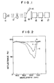
- the radiation image storage panel of the present invention provides an image of high sharpness when used in the method for recording and reproducing a radiation image shown in Figure 1.
- the photosensor 15 is used as a detector for detecting the light emitted by the panel 13, and reproduction of a radiation image is performed by means of the photosensor 15, the reproduction device 16 and the display device 17.
- means for reproducing a radiation image is not limited thereto.
- the object 12 is positioned between the radiation source 11 and the radiation image storage panel 13.
- the radiation passes through the object 12.
- the intensity of the radiation which has passed through the object 12 represents the transmittance of the object 12. Therefore, an image which represents the pattern of transmittance of the object 12 is obtained by means of the radiation impinging upon the radiation image storage panel 13.
- the radiation in the form of the image representing the pattern of transmittance of the object 12 is absorbed by the fluorescent layer of the panel 13, and electrons or holes are generated in the fluorescent layer.
- the amount of the electrons or holes generated are in proportion to the amount of the radiation absorbed.
- the electrons or holes are stored in the trap level of the stimulable phosphor, and thus, the radiation image is stored in the panel 13.
- the radiation stored in the panel 13 is visualized by stimulation with the stimulating rays emitted by the light source 14. That is, the fluorescent layer of the panel 13 is scanned with the stimulating rays emitted by the light source 14, whereby the electrons or holes stored in the trap level of the stimulable phosphor are expelled therefrom, and the radiation image stored in the panel 13 is released as fluorescent light.
- the panel 13 is colored with a colorant which selectively absorbs the stimulating rays, and therefore, when the fluorescent layer is scanned with the stimulating rays, the spread of the stimulating rays in the panel 13 due to irradiation in the fluorescent layer, halation in the protective layer, the primer layer or the substrate, or the like is controlled by the absorption of the stimulating rays by the colorant.
- the luminance of the fluorescent light emitted by the panel 13 is in proportion to the number of the electrons or holes stored in the fluorescent layer of the panel 13, that is, the amount of the radiation absorbed thereby.
- the fluorescent light (light signal) is detected and converted to an electrical signal sequentially by the photosensor 15 such as a photomultiplier.
- the electrical signal obtained is converted to an image signal corresponding to the radiation image by the reproduction device 16, and a visible image is displayed by the display device 17. Thus, the radiation image is reproduced.
- the spread of the stimulating rays in the panel is controlled by the absorption of the stimulating rays by the colorant contained in the panel. Therefore, the sharpness of the image reproduced by the reproduction device 16 and accordingly the sharpness of the image displayed by the display device 17 is markedly improved.
- BaFBr:Eu 2+ phosphor (stimulable phosphor) and one part by weight of nitrocellulose (binder) were mixed by use of a solvent (a mixture of acetone, ethyl acetate and butyl acetate) to prepare a coating dispersion having a viscosity of 50 centistokes.
- a dispersion comprising a methanol and Zapon Fast Blue 3G (organic blue colorant, manufactured by H8echst AG.) dispersed therein was prepared. Then, the dispersion was added to the coating dispersion in the ratio that the amount of the colorant was 1 milligram per 100 grams of the BaFBr:Eu 2+ phosphor.
- the coating dispersion containing the colorant- was uniformly applied to a polyethylene terephthalate film (substrate) positioned horizontally and dried naturally by allowing it to stand for a day to form a fluorescent layer of a thickness of about 300p.
- the radiation image storage panel thus obtained was named "Panel A”.
- Panel A and Panel B were exposed to X-rays of 80KVp and 250mA emitted by an X-ray source located at a distance of 180cm from the panels, and thereafter, the panels were scanned with a He-Ne laser beam (633nm).
- the light emitted by the fluorescent layer of the panels was detected and converted to an electrical signal by a photosensor (a photomultiplier having a spectral sensitivity of type S-5).
- the electrical signal obtained was converted to an image signal by a reproduction device, and a visible image was displayed by a display device.
- the modulation transfer function (MTF) of the image was obtained for both Panel A and Panel B.
- Table 1 shows that the MTF value of the respective images obtained by Panel A and Panel B and the relationship therebetween do not depend upon what type of the reproduction device and the display device are used.
- the curves a and b shown in Figure 2 are the reflection spectra of Panel A and Panel B, respectively, measured by an integrating-sphere photometer.
- Panel A very strongly absorbs a He-Ne laser beam having a wavelength of 633nm in comparison with Panel B.
- the absorbance of Panel A in the wavelength region of the light emitted by the BaFBr:Eu 2+ phosphor upon stimulation thereof is almost the same as that of Panel B (The spectrum of the light emitted by the BaFBr:Eu 2+ phosphor upon stimulation thereof is shown in Figure 3.). It is proved from these facts that the sharpness of Panel A is markedly high in comparison with Panel B as shown in Table 1, and that the sensitivity of Panel A is almost the same as that of Panel B.
- the dispersion was stirred for about 10 minutes and allowed to stand until the phosphor particles were precipitated, and the then resulting supernatant liquid was removed.
- the above-mentioned cycle was repeated several times until the supernatant liquid lost color. Thereafter, the precipitate was heated at a temperature of about 80°C to evaporate the methanol contained therein.
- the BaFBr:Eu 2+ phosphor bearing the blue colorant adsorbed on the surface thereof was obtained.
- Example 2 8 parts by weight of the BaFBr:Eu 2+ phosphor with the adsorbed blue colorant and one part by weight of nitrocellulose were mixed by use of the same solvent as mentioned in Example 1 to prepare a coating dispersion having a viscosity of 50 centistokes. Thereafter, the coating dispersion was uniformly applied to a polyethylene terephthalate film positioned horizontally and dried naturally by allowing it to stand for a day to form a fluorescent layer of a thickness of about 300p.
- the radiation image panel thus obtained was named "Panel C”.
- the MTF of Panel C was measured in the same manner as mentioned in Example 1. The result is shown in Table 1 below together with the MTF of Panel B.
- the curve C shown in Figure 2 is the reflection spectrum of Panel C measured by use of an integrating-sphere photometer.
- a radiation image storage panel was manufactured in the same manner as mentioned in Example 1 except for using Ultramarine Blue No. 1900 (inorganic blue colorant, manufactured by Daiichi Kasei Co., Ltd.) instead of Zapon Fast Blue 3G in the ratio that the amount of the colorant was 25 milligrams per 100 grams of the BaFBr:Eu 2+ phosphor.
- the radiation image storage panel thus obtained was named "Panel D”.
- a radiation image storage panel was manufactured in the same manner as mentioned in Example 1 except for using (Ba 0.9 ,Mg 0.1 )FCl:Ce 3+ phosphor and Cobalt Blue P (inorganic blue colorant, manufactured by Mitsubishi Kinzoku Co., Ltd.) instead of the BaFBr:Eu 2+ phosphor and Zapon Fast Blue 3G, respectively, in the ratio that the amount of the colorant was 50 milligrams per 100 grams of the (Ba 0.9 ,Mg 0.1 )FCl:Ce 3+ phosphor.
- the radiation image storage panel thus obtained was named "Panel E".
- a radiation image storage panel was manufactured in the same manner as mentioned in Example 1 except for using LaOBr:Ce 3+ ,Tb 3+ phosphor and Ultramarine Blue No.3000 (inorganic blue colorant, manufactured by Daiichi Kasei Co., Ltd.) instead of the BaFBr:Eu 2+ phosphor and Zapon Fast Blue 3G, respectively, in the ratio that the amount of the colorant was 25 milligrams per 100 grams of the LaOBr:Ce 3+ ,Tb 3+ phosphor.
- the radiation image storage panel thus obtained was named "Panel G".
- the radiation image storage panel of the present invention colored with a colorant provides a markedly sharp image than the conventional radiation image storage panel.
Landscapes
- Physics & Mathematics (AREA)
- General Physics & Mathematics (AREA)
- Engineering & Computer Science (AREA)
- General Engineering & Computer Science (AREA)
- High Energy & Nuclear Physics (AREA)
- Electromagnetism (AREA)
- Health & Medical Sciences (AREA)
- Life Sciences & Earth Sciences (AREA)
- Molecular Biology (AREA)
- Spectroscopy & Molecular Physics (AREA)
- Conversion Of X-Rays Into Visible Images (AREA)
- Radiography Using Non-Light Waves (AREA)
Applications Claiming Priority (2)
| Application Number | Priority Date | Filing Date | Title |
|---|---|---|---|
| JP71604/79 | 1979-06-07 | ||
| JP54071604A JPS5923400B2 (ja) | 1979-06-07 | 1979-06-07 | 放射線像変換パネル |
Publications (2)
| Publication Number | Publication Date |
|---|---|
| EP0021174A1 true EP0021174A1 (fr) | 1981-01-07 |
| EP0021174B1 EP0021174B1 (fr) | 1984-06-06 |
Family
ID=13465418
Family Applications (1)
| Application Number | Title | Priority Date | Filing Date |
|---|---|---|---|
| EP80103133A Expired EP0021174B1 (fr) | 1979-06-07 | 1980-06-05 | Panneau de mémoire pour image de radiation |
Country Status (4)
| Country | Link |
|---|---|
| US (1) | US4394581A (fr) |
| EP (1) | EP0021174B1 (fr) |
| JP (1) | JPS5923400B2 (fr) |
| DE (1) | DE3068099D1 (fr) |
Cited By (20)
| Publication number | Priority date | Publication date | Assignee | Title |
|---|---|---|---|---|
| FR2495818A1 (fr) * | 1980-12-05 | 1982-06-11 | Fuji Photo Film Co Ltd | Panneau de memorisation de rayonnement |
| DE3206776A1 (de) * | 1981-02-26 | 1982-10-28 | Eastman Kodak Co., 14650 Rochester, N.Y. | Roentgenverstaerkerschirm |
| EP0079791A1 (fr) * | 1981-11-13 | 1983-05-25 | Fuji Photo Film Co., Ltd. | Dispositif pour éteindre le bruit des feuilles phosphore à stimuler |
| EP0077678A3 (en) * | 1981-10-16 | 1983-09-07 | Fuji Photo Film Co., Ltd. | Radiation image recording and read-out system |
| EP0077677A3 (en) * | 1981-10-16 | 1983-09-07 | Fuji Photo Film Co., Ltd. | Radiation image read-out method and apparatus |
| EP0083085A3 (en) * | 1981-12-24 | 1983-09-21 | Fuji Photo Film Co., Ltd. | Radiation image recording and reproducing method |
| EP0094843A1 (fr) | 1982-05-19 | 1983-11-23 | Fuji Photo Film Co., Ltd. | Procédé et dispositif pour l'enregistrement et la reproduction d'image de rayonnement |
| EP0084818A3 (en) * | 1982-01-14 | 1984-03-07 | Fuji Photo Film Co., Ltd. | Radiation image storage panel |
| EP0158787A1 (fr) * | 1984-02-22 | 1985-10-23 | Kasei Optonix, Ltd. | Ecran renforçateur à gradient |
| US4587036A (en) * | 1983-12-27 | 1986-05-06 | Siemens Aktiengesellschaft | X-ray image storage screen |
| US4675271A (en) * | 1984-05-21 | 1987-06-23 | Siemens Aktiengesellschaft | Persistent screen for radiation images |
| US4696868A (en) * | 1984-10-17 | 1987-09-29 | Kasei Optonix, Ltd. | Intensifying screens |
| EP0167170A3 (en) * | 1984-07-04 | 1987-09-30 | Fuji Photo Film Co., Ltd. | Radiation image storage panel |
| EP0230324A3 (en) * | 1986-01-24 | 1988-07-13 | Kasei Optonix, Ltd. | Gradient radiation image conversion sheet |
| EP0291299A1 (fr) * | 1987-05-11 | 1988-11-17 | General Electric Company | Dispositif et méthode d'obtention d'une image à rayons X numérique |
| US4948696A (en) * | 1981-12-24 | 1990-08-14 | Fuji Photo Film Co., Ltd. | Radiation image recording and reproducing method |
| US6707057B2 (en) | 2000-03-23 | 2004-03-16 | Agfa-Gevaert | Storage phosphor screen with thick outermost layer and a method for using the same |
| US7396631B2 (en) | 2005-10-07 | 2008-07-08 | 3M Innovative Properties Company | Radiation curable thermal transfer elements |
| US7678526B2 (en) | 2005-10-07 | 2010-03-16 | 3M Innovative Properties Company | Radiation curable thermal transfer elements |
| EP2892055A4 (fr) * | 2012-08-29 | 2016-05-25 | Hamamatsu Photonics Kk | Panneau de conversion d'image de rayonnement |
Families Citing this family (50)
| Publication number | Priority date | Publication date | Assignee | Title |
|---|---|---|---|---|
| JPS5872044A (ja) * | 1981-10-27 | 1983-04-28 | Fuji Photo Film Co Ltd | 優先処理機能を備えた放射線画像情報記録再生システム |
| JPS5880633A (ja) * | 1981-11-09 | 1983-05-14 | Fuji Photo Film Co Ltd | 螢光体シ−トのノイズ消去方法および装置 |
| JPS58161900A (ja) * | 1982-03-19 | 1983-09-26 | キヤノン株式会社 | 感度変化を有する螢光スクリーン及び該螢光スクリーンを用いたx線装置 |
| JPS58163340A (ja) * | 1982-03-20 | 1983-09-28 | 富士写真フイルム株式会社 | 放射線画像のサブトラクシヨン処理方法 |
| JPS58182600A (ja) * | 1982-04-20 | 1983-10-25 | 富士写真フイルム株式会社 | 放射線像変換パネル |
| JPS58200231A (ja) * | 1982-05-18 | 1983-11-21 | Fuji Photo Film Co Ltd | 放射線画像情報記録再生方法におけるノイズ消去方法 |
| JPS5942500A (ja) * | 1982-09-01 | 1984-03-09 | 富士写真フイルム株式会社 | 放射線像変換パネル |
| JPS5956480A (ja) * | 1982-09-27 | 1984-03-31 | Fuji Photo Film Co Ltd | 蛍光体およびそれを用いた放射線像変換パネル |
| JPS59139000A (ja) * | 1983-01-31 | 1984-08-09 | 富士写真フイルム株式会社 | 放射線像変換方法 |
| JPS59162498A (ja) * | 1983-03-07 | 1984-09-13 | 富士写真フイルム株式会社 | 放射線像変換パネル |
| JPS59162499A (ja) * | 1983-03-07 | 1984-09-13 | 富士写真フイルム株式会社 | 放射線像変換パネル |
| JPS6013299A (ja) * | 1983-07-05 | 1985-01-23 | コニカ株式会社 | 放射線画像変換パネル |
| US4603253A (en) * | 1983-10-19 | 1986-07-29 | Kabushiki Kaisha Toshiba | Radiation image converting panel and an apparatus for reading out a radiation image from the same |
| CA1235569A (fr) | 1983-12-28 | 1988-04-26 | Nobufumi Mori | Luminophore et panneau de stockage d'images utilisant ce luminophore |
| US4684592A (en) * | 1984-04-06 | 1987-08-04 | Fuji Photo Film Co., Ltd. | Stimulable phosphor sheet |
| JPS60163070U (ja) * | 1984-04-09 | 1985-10-29 | 有限会社 いのうえ寝装 | 羽毛布団用羽毛充填装置 |
| JPS60222034A (ja) * | 1984-04-18 | 1985-11-06 | 富士写真フイルム株式会社 | エネルギ−サブトラクシヨンにおける画像形成方法 |
| JPS60260035A (ja) * | 1984-06-06 | 1985-12-23 | Fuji Photo Film Co Ltd | 蓄積性螢光体シ−トの残像消去方法および装置 |
| US4665003A (en) * | 1984-07-31 | 1987-05-12 | Fuji Photo Film Co., Ltd. | Stimulable phosphor sheet and method of conveying the same |
| DE3578081D1 (de) | 1984-09-14 | 1990-07-12 | Konishiroku Photo Ind | Verfahren zur umwandlung eines radiographischen bildes und schirm zum speichern einer strahlungsenergie mit einer anregbaren phosphorschicht. |
| JPS61138441A (ja) * | 1984-11-29 | 1986-06-25 | Fuji Photo Film Co Ltd | 電子顕微鏡像記録再生方法 |
| US4851677A (en) * | 1984-12-07 | 1989-07-25 | Fuji Photo Co., Ltd. | Apparatus for recording and reproducing image produced by an electron microscope including an optical filter and a deflecting element |
| DE3587871T2 (de) * | 1984-12-10 | 1994-10-13 | Fuji Photo Film Co Ltd | Verfahren zur Feststellung eines Fokussierungsfehlers eines elektronen-mikroskopischen Bildes. |
| JPS61228399A (ja) * | 1985-04-03 | 1986-10-11 | 富士写真フイルム株式会社 | 放射線像変換パネルおよびその製法 |
| JPH0631905B2 (ja) * | 1985-04-30 | 1994-04-27 | コニカ株式会社 | 放射線画像変換パネル |
| US4835386A (en) | 1985-10-18 | 1989-05-30 | Fuji Photo Film Co., Ltd. | Radiation image recording and read-out apparatus |
| EP0233497B1 (fr) * | 1986-01-21 | 1990-05-09 | Fuji Photo Film Co., Ltd. | Panneau de mémorisation d'image de rayonnement |
| EP0230314B1 (fr) * | 1986-01-21 | 1992-05-13 | Fuji Photo Film Co., Ltd. | Ecran pour l'enregistrement d'une image obtenue par rayonnement |
| JPH0690319B2 (ja) * | 1987-02-02 | 1994-11-14 | 富士写真フイルム株式会社 | 放射線像変換パネルの製造法 |
| US4879202A (en) | 1986-07-11 | 1989-11-07 | Fuji Photo Film Co., Ltd. | Radiation image storage panel and process for the preparation of the same |
| US5340996A (en) * | 1989-08-10 | 1994-08-23 | Fuji Photo Film Co., Ltd. | Radiation image read-out apparatus, radiation image recording method and apparatus, stimulable phosphor sheet, and cassette |
| US4999505A (en) * | 1990-02-08 | 1991-03-12 | Eastman Kodak Company | Transparent radiation image storage panel |
| US5483081A (en) * | 1992-10-19 | 1996-01-09 | Fuji Photo Film Co., Ltd. | Method for detecting light emitted by two surfaces of a stimulable phosphor sheet |
| JP3515169B2 (ja) * | 1994-04-15 | 2004-04-05 | 富士写真フイルム株式会社 | 放射線像記録再生方法および放射線像変換パネル |
| US5520965A (en) * | 1994-10-07 | 1996-05-28 | Minnesota Mining And Manufacturing Company | Radiation cured radiographic intensifying screen |
| US5725989A (en) | 1996-04-15 | 1998-03-10 | Chang; Jeffrey C. | Laser addressable thermal transfer imaging element with an interlayer |
| US7534543B2 (en) | 1996-04-15 | 2009-05-19 | 3M Innovative Properties Company | Texture control of thin film layers prepared via laser induced thermal imaging |
| US5998085A (en) * | 1996-07-23 | 1999-12-07 | 3M Innovative Properties | Process for preparing high resolution emissive arrays and corresponding articles |
| EP1065525A3 (fr) * | 1999-07-02 | 2006-04-05 | Agfa-Gevaert | Dispositif pour la reproduction d'images de rayonnement |
| JP2001083641A (ja) | 1999-09-17 | 2001-03-30 | Fuji Photo Film Co Ltd | 放射線画像読取装置 |
| DE10116803C2 (de) * | 2001-04-04 | 2003-10-02 | Siemens Ag | Strahlungswandler und Verfahren zur Herstellung desselben |
| EP1316971A3 (fr) * | 2001-12-03 | 2007-03-28 | Agfa-Gevaert | Ecran luminescent sans liant sur un support coloré par un mélange de pigments |
| US20030134087A1 (en) * | 2001-12-03 | 2003-07-17 | Ludo Joly | Binderless phosphor screen on a support colored with a pigment mixture |
| US6977385B2 (en) * | 2002-03-26 | 2005-12-20 | Agfa-Gevaert | Storage phosphor screen having binderless colored layers |
| US7029819B2 (en) * | 2003-11-12 | 2006-04-18 | Eastman Kodak Company | Phosphor screen and imaging assembly |
| JP4765292B2 (ja) * | 2004-01-06 | 2011-09-07 | コニカミノルタエムジー株式会社 | 放射線画像読取方法及び放射線画像読取装置並びに輝尽性蛍光体プレート |
| JP4587843B2 (ja) * | 2005-02-28 | 2010-11-24 | 独立行政法人 日本原子力研究開発機構 | ガラス状化イメージングプレート |
| FI20086241A7 (fi) | 2008-12-23 | 2010-06-24 | Palodex Group Oy | Kuvalevyn lukijalaite |
| FI20086240A7 (fi) | 2008-12-23 | 2010-06-24 | Palodex Group Oy | Kuvalevyn lukijalaitteen puhdistusjärjestelmä |
| JP5883556B2 (ja) | 2010-06-04 | 2016-03-15 | 浜松ホトニクス株式会社 | 放射線イメージセンサ |
Citations (6)
| Publication number | Priority date | Publication date | Assignee | Title |
|---|---|---|---|---|
| DE1764329B2 (de) * | 1967-05-17 | 1974-01-10 | Thorn Electrical Industries Ltd., London | Festkörper Bildspeicher, insbe sondere zur Verwendung mit Röntgen strahlen als Anregungsstrahlung |
| US3859527A (en) * | 1973-01-02 | 1975-01-07 | Eastman Kodak Co | Apparatus and method for producing images corresponding to patterns of high energy radiation |
| US3883747A (en) * | 1973-12-06 | 1975-05-13 | Minnesota Mining & Mfg | X-ray intensifying screen |
| US3975637A (en) * | 1973-10-23 | 1976-08-17 | Matsushita Electric Industrial Co., Ltd. | Device for storage and display of a radiation image |
| DE2638768A1 (de) * | 1975-08-28 | 1977-03-03 | Dainippon Toryo Kk | Verstaerkerschirm fuer die radiographie |
| US4028550A (en) * | 1975-12-22 | 1977-06-07 | E. I. Du Pont De Nemours And Company | X-ray screens |
Family Cites Families (1)
| Publication number | Priority date | Publication date | Assignee | Title |
|---|---|---|---|---|
| US4012637A (en) * | 1975-05-05 | 1977-03-15 | General Electric Company | Radiographic screen with improved resolution |
-
1979
- 1979-06-07 JP JP54071604A patent/JPS5923400B2/ja not_active Expired
-
1980
- 1980-06-05 DE DE8080103133T patent/DE3068099D1/de not_active Expired
- 1980-06-05 US US06/156,520 patent/US4394581A/en not_active Expired - Lifetime
- 1980-06-05 EP EP80103133A patent/EP0021174B1/fr not_active Expired
Patent Citations (6)
| Publication number | Priority date | Publication date | Assignee | Title |
|---|---|---|---|---|
| DE1764329B2 (de) * | 1967-05-17 | 1974-01-10 | Thorn Electrical Industries Ltd., London | Festkörper Bildspeicher, insbe sondere zur Verwendung mit Röntgen strahlen als Anregungsstrahlung |
| US3859527A (en) * | 1973-01-02 | 1975-01-07 | Eastman Kodak Co | Apparatus and method for producing images corresponding to patterns of high energy radiation |
| US3975637A (en) * | 1973-10-23 | 1976-08-17 | Matsushita Electric Industrial Co., Ltd. | Device for storage and display of a radiation image |
| US3883747A (en) * | 1973-12-06 | 1975-05-13 | Minnesota Mining & Mfg | X-ray intensifying screen |
| DE2638768A1 (de) * | 1975-08-28 | 1977-03-03 | Dainippon Toryo Kk | Verstaerkerschirm fuer die radiographie |
| US4028550A (en) * | 1975-12-22 | 1977-06-07 | E. I. Du Pont De Nemours And Company | X-ray screens |
Cited By (23)
| Publication number | Priority date | Publication date | Assignee | Title |
|---|---|---|---|---|
| FR2495818A1 (fr) * | 1980-12-05 | 1982-06-11 | Fuji Photo Film Co Ltd | Panneau de memorisation de rayonnement |
| DE3206776A1 (de) * | 1981-02-26 | 1982-10-28 | Eastman Kodak Co., 14650 Rochester, N.Y. | Roentgenverstaerkerschirm |
| EP0077678A3 (en) * | 1981-10-16 | 1983-09-07 | Fuji Photo Film Co., Ltd. | Radiation image recording and read-out system |
| EP0077677A3 (en) * | 1981-10-16 | 1983-09-07 | Fuji Photo Film Co., Ltd. | Radiation image read-out method and apparatus |
| EP0079791A1 (fr) * | 1981-11-13 | 1983-05-25 | Fuji Photo Film Co., Ltd. | Dispositif pour éteindre le bruit des feuilles phosphore à stimuler |
| EP0083085A3 (en) * | 1981-12-24 | 1983-09-21 | Fuji Photo Film Co., Ltd. | Radiation image recording and reproducing method |
| US4948696A (en) * | 1981-12-24 | 1990-08-14 | Fuji Photo Film Co., Ltd. | Radiation image recording and reproducing method |
| EP0084818A3 (en) * | 1982-01-14 | 1984-03-07 | Fuji Photo Film Co., Ltd. | Radiation image storage panel |
| EP0094843A1 (fr) | 1982-05-19 | 1983-11-23 | Fuji Photo Film Co., Ltd. | Procédé et dispositif pour l'enregistrement et la reproduction d'image de rayonnement |
| EP0094843B2 (fr) † | 1982-05-19 | 1991-09-04 | Fuji Photo Film Co., Ltd. | Procédé et dispositif pour l'enregistrement et la reproduction d'image de rayonnement |
| US4587036A (en) * | 1983-12-27 | 1986-05-06 | Siemens Aktiengesellschaft | X-ray image storage screen |
| EP0158787A1 (fr) * | 1984-02-22 | 1985-10-23 | Kasei Optonix, Ltd. | Ecran renforçateur à gradient |
| US4772803A (en) * | 1984-02-22 | 1988-09-20 | Kasei Optonix, Ltd. | Gradient intensifying screen |
| US4675271A (en) * | 1984-05-21 | 1987-06-23 | Siemens Aktiengesellschaft | Persistent screen for radiation images |
| EP0167170A3 (en) * | 1984-07-04 | 1987-09-30 | Fuji Photo Film Co., Ltd. | Radiation image storage panel |
| US4696868A (en) * | 1984-10-17 | 1987-09-29 | Kasei Optonix, Ltd. | Intensifying screens |
| EP0230324A3 (en) * | 1986-01-24 | 1988-07-13 | Kasei Optonix, Ltd. | Gradient radiation image conversion sheet |
| US4816350A (en) * | 1986-01-24 | 1989-03-28 | Kasei Optonix Ltd. | Gradient radiation image conversion sheet |
| EP0291299A1 (fr) * | 1987-05-11 | 1988-11-17 | General Electric Company | Dispositif et méthode d'obtention d'une image à rayons X numérique |
| US6707057B2 (en) | 2000-03-23 | 2004-03-16 | Agfa-Gevaert | Storage phosphor screen with thick outermost layer and a method for using the same |
| US7396631B2 (en) | 2005-10-07 | 2008-07-08 | 3M Innovative Properties Company | Radiation curable thermal transfer elements |
| US7678526B2 (en) | 2005-10-07 | 2010-03-16 | 3M Innovative Properties Company | Radiation curable thermal transfer elements |
| EP2892055A4 (fr) * | 2012-08-29 | 2016-05-25 | Hamamatsu Photonics Kk | Panneau de conversion d'image de rayonnement |
Also Published As
| Publication number | Publication date |
|---|---|
| JPS5923400B2 (ja) | 1984-06-01 |
| JPS55163500A (en) | 1980-12-19 |
| DE3068099D1 (en) | 1984-07-12 |
| US4394581A (en) | 1983-07-19 |
| EP0021174B1 (fr) | 1984-06-06 |
Similar Documents
| Publication | Publication Date | Title |
|---|---|---|
| US4394581A (en) | Radiation image storage panel | |
| US4380702A (en) | Radiation image storage panel | |
| US4491736A (en) | Radiation image storage panel | |
| US4368390A (en) | Radiation image storage panel | |
| US4350893A (en) | Radiation image storage panel | |
| US5198679A (en) | Phosphor and image storage panel | |
| US5023014A (en) | Phosphor | |
| US4571496A (en) | Radiation image storage panel | |
| EP0084818B1 (fr) | Panneau d'accumulation pour image de radiation | |
| US5534710A (en) | Radiation image storage panel and radiation image reading method | |
| US4950559A (en) | Radiation image storage panel | |
| US5591982A (en) | Radiation image storage panel and radiation image recording and reproducing method | |
| US5880476A (en) | Radiation image storage panel and radiation image reading method | |
| US4780376A (en) | Phosphor and radiation image storage panel | |
| EP0158862B1 (fr) | Ecran pour l'enregistrement d'une image obtenue par rayonnement | |
| US4789785A (en) | Radiation image converting material | |
| EP0118880B1 (fr) | Ecran pour l'enregistrement d'une image obtenue par rayonnement | |
| US4621196A (en) | Radiation image storage panel | |
| US4628208A (en) | Radiation image storage panel | |
| US4801806A (en) | Radiation image recording and reproducing method | |
| EP0143301B1 (fr) | Matière luminescente, méthode d'enregistrement et de reproduction d'une image obtenue par rayonnement et écran pour l'enregistrement d'une image obtenue par rayonnement au moyen de cette méthode | |
| US4698508A (en) | Phosphor, radiation image recording and reproducing method and radiation image storage panel | |
| JP2583417B2 (ja) | 放射線像形成方法 | |
| EP0163144B1 (fr) | Matière luminescente, méthode d'enregistrement et de restitution d'une image obtenue par rayonnement et écran pour l'enregistrement d'une image obtenue par rayonnement | |
| JPH0664196B2 (ja) | 放射線画像変換パネル |
Legal Events
| Date | Code | Title | Description |
|---|---|---|---|
| PUAI | Public reference made under article 153(3) epc to a published international application that has entered the european phase |
Free format text: ORIGINAL CODE: 0009012 |
|
| AK | Designated contracting states |
Designated state(s): DE FR NL |
|
| DET | De: translation of patent claims | ||
| 17P | Request for examination filed |
Effective date: 19810703 |
|
| GRAA | (expected) grant |
Free format text: ORIGINAL CODE: 0009210 |
|
| AK | Designated contracting states |
Designated state(s): DE FR NL |
|
| REF | Corresponds to: |
Ref document number: 3068099 Country of ref document: DE Date of ref document: 19840712 |
|
| ET | Fr: translation filed | ||
| PLBE | No opposition filed within time limit |
Free format text: ORIGINAL CODE: 0009261 |
|
| STAA | Information on the status of an ep patent application or granted ep patent |
Free format text: STATUS: NO OPPOSITION FILED WITHIN TIME LIMIT |
|
| 26N | No opposition filed | ||
| PGFP | Annual fee paid to national office [announced via postgrant information from national office to epo] |
Ref country code: FR Payment date: 19990616 Year of fee payment: 20 |
|
| PGFP | Annual fee paid to national office [announced via postgrant information from national office to epo] |
Ref country code: NL Payment date: 19990622 Year of fee payment: 20 |
|
| PGFP | Annual fee paid to national office [announced via postgrant information from national office to epo] |
Ref country code: DE Payment date: 19990728 Year of fee payment: 20 |
|
| PG25 | Lapsed in a contracting state [announced via postgrant information from national office to epo] |
Ref country code: NL Free format text: LAPSE BECAUSE OF EXPIRATION OF PROTECTION Effective date: 20000605 |
|
| NLV7 | Nl: ceased due to reaching the maximum lifetime of a patent |
Effective date: 20000605 |