EP0025717A2 - Dispositif semiconducteur comprenant deux couches isolantes et procédé pour le fabriquer - Google Patents
Dispositif semiconducteur comprenant deux couches isolantes et procédé pour le fabriquer Download PDFInfo
- Publication number
- EP0025717A2 EP0025717A2 EP80303242A EP80303242A EP0025717A2 EP 0025717 A2 EP0025717 A2 EP 0025717A2 EP 80303242 A EP80303242 A EP 80303242A EP 80303242 A EP80303242 A EP 80303242A EP 0025717 A2 EP0025717 A2 EP 0025717A2
- Authority
- EP
- European Patent Office
- Prior art keywords
- film
- oxygen
- nitrogen
- source
- semiconductor device
- Prior art date
- Legal status (The legal status is an assumption and is not a legal conclusion. Google has not performed a legal analysis and makes no representation as to the accuracy of the status listed.)
- Granted
Links
Images


Classifications
-
- H—ELECTRICITY
- H10—SEMICONDUCTOR DEVICES; ELECTRIC SOLID-STATE DEVICES NOT OTHERWISE PROVIDED FOR
- H10P—GENERIC PROCESSES OR APPARATUS FOR THE MANUFACTURE OR TREATMENT OF DEVICES COVERED BY CLASS H10
- H10P14/00—Formation of materials, e.g. in the shape of layers or pillars
- H10P14/60—Formation of materials, e.g. in the shape of layers or pillars of insulating materials
- H10P14/69—Inorganic materials
- H10P14/692—Inorganic materials composed of oxides, glassy oxides or oxide-based glasses
- H10P14/6921—Inorganic materials composed of oxides, glassy oxides or oxide-based glasses containing silicon
- H10P14/6922—Inorganic materials composed of oxides, glassy oxides or oxide-based glasses containing silicon the material containing Si, O and at least one of H, N, C, F or other non-metal elements, e.g. SiOC, SiOC:H or SiONC
- H10P14/6927—Inorganic materials composed of oxides, glassy oxides or oxide-based glasses containing silicon the material containing Si, O and at least one of H, N, C, F or other non-metal elements, e.g. SiOC, SiOC:H or SiONC the material being a silicon oxynitride, e.g. SiON or SiON:H
-
- C—CHEMISTRY; METALLURGY
- C23—COATING METALLIC MATERIAL; COATING MATERIAL WITH METALLIC MATERIAL; CHEMICAL SURFACE TREATMENT; DIFFUSION TREATMENT OF METALLIC MATERIAL; COATING BY VACUUM EVAPORATION, BY SPUTTERING, BY ION IMPLANTATION OR BY CHEMICAL VAPOUR DEPOSITION, IN GENERAL; INHIBITING CORROSION OF METALLIC MATERIAL OR INCRUSTATION IN GENERAL
- C23C—COATING METALLIC MATERIAL; COATING MATERIAL WITH METALLIC MATERIAL; SURFACE TREATMENT OF METALLIC MATERIAL BY DIFFUSION INTO THE SURFACE, BY CHEMICAL CONVERSION OR SUBSTITUTION; COATING BY VACUUM EVAPORATION, BY SPUTTERING, BY ION IMPLANTATION OR BY CHEMICAL VAPOUR DEPOSITION, IN GENERAL
- C23C16/00—Chemical coating by decomposition of gaseous compounds, without leaving reaction products of surface material in the coating, i.e. chemical vapour deposition [CVD] processes
- C23C16/22—Chemical coating by decomposition of gaseous compounds, without leaving reaction products of surface material in the coating, i.e. chemical vapour deposition [CVD] processes characterised by the deposition of inorganic material, other than metallic material
- C23C16/30—Deposition of compounds, mixtures or solid solutions, e.g. borides, carbides, nitrides
- C23C16/308—Oxynitrides
-
- H—ELECTRICITY
- H10—SEMICONDUCTOR DEVICES; ELECTRIC SOLID-STATE DEVICES NOT OTHERWISE PROVIDED FOR
- H10D—INORGANIC ELECTRIC SEMICONDUCTOR DEVICES
- H10D30/00—Field-effect transistors [FET]
- H10D30/60—Insulated-gate field-effect transistors [IGFET]
- H10D30/68—Floating-gate IGFETs
- H10D30/681—Floating-gate IGFETs having only two programming levels
-
- H—ELECTRICITY
- H10—SEMICONDUCTOR DEVICES; ELECTRIC SOLID-STATE DEVICES NOT OTHERWISE PROVIDED FOR
- H10D—INORGANIC ELECTRIC SEMICONDUCTOR DEVICES
- H10D64/00—Electrodes of devices having potential barriers
- H10D64/60—Electrodes characterised by their materials
- H10D64/66—Electrodes having a conductor capacitively coupled to a semiconductor by an insulator, e.g. MIS electrodes
- H10D64/68—Electrodes having a conductor capacitively coupled to a semiconductor by an insulator, e.g. MIS electrodes characterised by the insulator, e.g. by the gate insulator
- H10D64/693—Electrodes having a conductor capacitively coupled to a semiconductor by an insulator, e.g. MIS electrodes characterised by the insulator, e.g. by the gate insulator the insulator comprising nitrogen, e.g. nitrides, oxynitrides or nitrogen-doped materials
-
- H—ELECTRICITY
- H10—SEMICONDUCTOR DEVICES; ELECTRIC SOLID-STATE DEVICES NOT OTHERWISE PROVIDED FOR
- H10P—GENERIC PROCESSES OR APPARATUS FOR THE MANUFACTURE OR TREATMENT OF DEVICES COVERED BY CLASS H10
- H10P14/00—Formation of materials, e.g. in the shape of layers or pillars
- H10P14/60—Formation of materials, e.g. in the shape of layers or pillars of insulating materials
- H10P14/63—Formation of materials, e.g. in the shape of layers or pillars of insulating materials characterised by the formation processes
- H10P14/6326—Deposition processes
- H10P14/6328—Deposition from the gas or vapour phase
- H10P14/6334—Deposition from the gas or vapour phase using decomposition or reaction of gaseous or vapour phase compounds, i.e. chemical vapour deposition
- H10P14/6336—Deposition from the gas or vapour phase using decomposition or reaction of gaseous or vapour phase compounds, i.e. chemical vapour deposition in the presence of a plasma [PECVD]
-
- H—ELECTRICITY
- H10—SEMICONDUCTOR DEVICES; ELECTRIC SOLID-STATE DEVICES NOT OTHERWISE PROVIDED FOR
- H10W—GENERIC PACKAGES, INTERCONNECTIONS, CONNECTORS OR OTHER CONSTRUCTIONAL DETAILS OF DEVICES COVERED BY CLASS H10
- H10W74/00—Encapsulations, e.g. protective coatings
- H10W74/01—Manufacture or treatment
-
- H—ELECTRICITY
- H10—SEMICONDUCTOR DEVICES; ELECTRIC SOLID-STATE DEVICES NOT OTHERWISE PROVIDED FOR
- H10W—GENERIC PACKAGES, INTERCONNECTIONS, CONNECTORS OR OTHER CONSTRUCTIONAL DETAILS OF DEVICES COVERED BY CLASS H10
- H10W74/00—Encapsulations, e.g. protective coatings
- H10W74/10—Encapsulations, e.g. protective coatings characterised by their shape or disposition
- H10W74/131—Encapsulations, e.g. protective coatings characterised by their shape or disposition the semiconductor body being only partially enclosed
- H10W74/137—Encapsulations, e.g. protective coatings characterised by their shape or disposition the semiconductor body being only partially enclosed the encapsulations being directly on the semiconductor body
-
- H—ELECTRICITY
- H10—SEMICONDUCTOR DEVICES; ELECTRIC SOLID-STATE DEVICES NOT OTHERWISE PROVIDED FOR
- H10W—GENERIC PACKAGES, INTERCONNECTIONS, CONNECTORS OR OTHER CONSTRUCTIONAL DETAILS OF DEVICES COVERED BY CLASS H10
- H10W74/00—Encapsulations, e.g. protective coatings
- H10W74/40—Encapsulations, e.g. protective coatings characterised by their materials
- H10W74/43—Encapsulations, e.g. protective coatings characterised by their materials comprising oxides, nitrides or carbides, e.g. ceramics or glasses
-
- H—ELECTRICITY
- H10—SEMICONDUCTOR DEVICES; ELECTRIC SOLID-STATE DEVICES NOT OTHERWISE PROVIDED FOR
- H10P—GENERIC PROCESSES OR APPARATUS FOR THE MANUFACTURE OR TREATMENT OF DEVICES COVERED BY CLASS H10
- H10P14/00—Formation of materials, e.g. in the shape of layers or pillars
- H10P14/60—Formation of materials, e.g. in the shape of layers or pillars of insulating materials
- H10P14/63—Formation of materials, e.g. in the shape of layers or pillars of insulating materials characterised by the formation processes
- H10P14/6326—Deposition processes
- H10P14/6328—Deposition from the gas or vapour phase
- H10P14/6329—Deposition from the gas or vapour phase using physical ablation of a target, e.g. physical vapour deposition or pulsed laser deposition
-
- H—ELECTRICITY
- H10—SEMICONDUCTOR DEVICES; ELECTRIC SOLID-STATE DEVICES NOT OTHERWISE PROVIDED FOR
- H10P—GENERIC PROCESSES OR APPARATUS FOR THE MANUFACTURE OR TREATMENT OF DEVICES COVERED BY CLASS H10
- H10P14/00—Formation of materials, e.g. in the shape of layers or pillars
- H10P14/60—Formation of materials, e.g. in the shape of layers or pillars of insulating materials
- H10P14/69—Inorganic materials
- H10P14/694—Inorganic materials composed of nitrides
- H10P14/6943—Inorganic materials composed of nitrides containing silicon
- H10P14/69433—Inorganic materials composed of nitrides containing silicon the material being a silicon nitride not containing oxygen, e.g. SixNy or SixByNz
-
- Y—GENERAL TAGGING OF NEW TECHNOLOGICAL DEVELOPMENTS; GENERAL TAGGING OF CROSS-SECTIONAL TECHNOLOGIES SPANNING OVER SEVERAL SECTIONS OF THE IPC; TECHNICAL SUBJECTS COVERED BY FORMER USPC CROSS-REFERENCE ART COLLECTIONS [XRACs] AND DIGESTS
- Y10—TECHNICAL SUBJECTS COVERED BY FORMER USPC
- Y10S—TECHNICAL SUBJECTS COVERED BY FORMER USPC CROSS-REFERENCE ART COLLECTIONS [XRACs] AND DIGESTS
- Y10S148/00—Metal treatment
- Y10S148/043—Dual dielectric
-
- Y—GENERAL TAGGING OF NEW TECHNOLOGICAL DEVELOPMENTS; GENERAL TAGGING OF CROSS-SECTIONAL TECHNOLOGIES SPANNING OVER SEVERAL SECTIONS OF THE IPC; TECHNICAL SUBJECTS COVERED BY FORMER USPC CROSS-REFERENCE ART COLLECTIONS [XRACs] AND DIGESTS
- Y10—TECHNICAL SUBJECTS COVERED BY FORMER USPC
- Y10S—TECHNICAL SUBJECTS COVERED BY FORMER USPC CROSS-REFERENCE ART COLLECTIONS [XRACs] AND DIGESTS
- Y10S148/00—Metal treatment
- Y10S148/081—Insulators
-
- Y—GENERAL TAGGING OF NEW TECHNOLOGICAL DEVELOPMENTS; GENERAL TAGGING OF CROSS-SECTIONAL TECHNOLOGIES SPANNING OVER SEVERAL SECTIONS OF THE IPC; TECHNICAL SUBJECTS COVERED BY FORMER USPC CROSS-REFERENCE ART COLLECTIONS [XRACs] AND DIGESTS
- Y10—TECHNICAL SUBJECTS COVERED BY FORMER USPC
- Y10S—TECHNICAL SUBJECTS COVERED BY FORMER USPC CROSS-REFERENCE ART COLLECTIONS [XRACs] AND DIGESTS
- Y10S148/00—Metal treatment
- Y10S148/114—Nitrides of silicon
-
- Y—GENERAL TAGGING OF NEW TECHNOLOGICAL DEVELOPMENTS; GENERAL TAGGING OF CROSS-SECTIONAL TECHNOLOGIES SPANNING OVER SEVERAL SECTIONS OF THE IPC; TECHNICAL SUBJECTS COVERED BY FORMER USPC CROSS-REFERENCE ART COLLECTIONS [XRACs] AND DIGESTS
- Y10—TECHNICAL SUBJECTS COVERED BY FORMER USPC
- Y10S—TECHNICAL SUBJECTS COVERED BY FORMER USPC CROSS-REFERENCE ART COLLECTIONS [XRACs] AND DIGESTS
- Y10S438/00—Semiconductor device manufacturing: process
- Y10S438/958—Passivation layer
-
- Y—GENERAL TAGGING OF NEW TECHNOLOGICAL DEVELOPMENTS; GENERAL TAGGING OF CROSS-SECTIONAL TECHNOLOGIES SPANNING OVER SEVERAL SECTIONS OF THE IPC; TECHNICAL SUBJECTS COVERED BY FORMER USPC CROSS-REFERENCE ART COLLECTIONS [XRACs] AND DIGESTS
- Y10—TECHNICAL SUBJECTS COVERED BY FORMER USPC
- Y10S—TECHNICAL SUBJECTS COVERED BY FORMER USPC CROSS-REFERENCE ART COLLECTIONS [XRACs] AND DIGESTS
- Y10S438/00—Semiconductor device manufacturing: process
- Y10S438/972—Stored charge erasure
Definitions
- the present invention relates to a semiconductor device, in which active and passive elements are formed on a semiconductor substrate, more particularly, a semiconductor device, wherein-the semiconductor substrate is covered by an insulating film, for example, an ultraviolet-erasable, electrically alterable read-only memory (hereinafter referred to as EPROM) device, as well as a process for producing the same.
- an insulating film for example, an ultraviolet-erasable, electrically alterable read-only memory (hereinafter referred to as EPROM) device, as well as a process for producing the same.
- EPROM ultraviolet-erasable, electrically alterable read-only memory
- a semiconductor device for example, an EP R OM device
- a surface passivation film usually consisting of a phosphosilicate glass (PSG)
- PSG phosphosilicate glass
- a silicon nitride (Si 3 N 4 ) film formed by a plasma vapor phase growth method is finding use as a surface passivation film for semiconductor elements, because silicon nitride is superior in moisture proofness to PSG.
- the silicon nitride has an absorption edge at a wave length of about 2800 A , which causes the silicon nitride to be impermeable to ultraviolet rays. Accordingly, the silicon nitride film is not usable as a surface passivation film for the EPROM device whose memory is erased by ultraviolet rays 0 whose central wave length is 2537 A .
- a semiconductor device comprises a semiconductor substrate, at least one active and/or passive element formed on or in the substrate, a first insulating film located on the substrate, leading electrodes of at least one said element, and a second insulating film covering the at least one element, the first insulating film and the leading electrodes, characterised in that the second insulating film comprises an oxynitride having an oxygen atom percentage, based on the total of the oxygen and nitrogen atoms in the oxygen containing silicon nitride film, of from 20 to 70%.
- the layer that serves as the second insulating film preferably consists solely of the oxynitride film.
- the invention includes also processes for producing a semiconductor device by forming a passivation film on the device.
- the device may be a novel semiconductor device as described above or may be other semiconductor devices, as described below.
- One method according to the invention comprises contacting a silicon substrate with an atmosphere containing ammonia or, less preferably, nitrogen, as a source of nitrogen and nitrous oxide, or less preferably, oxygen, as a source of oxygen, at elevated temperature.
- the feed gas may, in some methods, be monosilane or may be an inert gas such as argon.
- the ratio of nitrous oxide to ammonia + nitrous oxide is in the range 0.1 to 0.5 and preferably the oxygen atom percentage of the oxynitride film that is formed is, based on the total of oxygen and nitrogen atoms in the oxynitride from 20 to 70%.
- the passivation film is formed by chemical vapour deposition using monosilane as a feed gas, ammonia (or less preferably nitrogen) as a source of nitrogen, and nitrous oxide as a source of oxygen, with the ratio of N 2 0 to NH 3 + N 2 0 being in the range of 0.1 to 0.5 .
- This process may be carried out at high temperatures, preferably 700 to 800°C but it is particularly advantageous to carry out the method by a-plasma chemical vapour deposition method in which event the temperature, while still being elevated, can be rather lower, for instance 250°C to 450°C.
- Another method for forming a surface passivation film according to the invention is a reactive sputtering method in which silicon is used as a target, ammonia or nitrogen is used as a source of nitrogen and oxygen or nitrous oxide is used as its source of oxygen.
- ammonia and nitrous oxide are used and preferably the ratio N 2 0 to NH 3 + N 2 0 is from 0.1 to 0.5 .
- FIG. 1 there is shown a cross-sectional view of the memory cell part of an EPROM element.
- a p-type silicon semiconductor substrate is represented at 1 and N +- type source and drain regions are represented at 2 and 3, respectively, which regions are formed on the surface regions of the silicon semicondcutor substrate 1.
- a field insulating film (first insulating film) 4 consisting of a silicon oxide(Si0 2 ) film isolates individual ERROM elements (memory cells) from each other.
- a floating gate 7 consisting of polycrystalline silicon and a control gate 8 consisting of polycrystalline silicon are embedded within an insulating film (first insulating film) 9.
- a surface passivation film (second insulating film) 10 is provided on the surface of the EPROM device.
- the above-mentioned structure of the memory cell of an EPROM device is known.
- the EPROM device is subjected to irradiation of ultraviolet rays through the surface passivation film 10 to discharge the electric charge stored in the floating gate 8 toward the substrate 1.
- the surface passivation film 10 PSG has been mainly used heretofore.
- the PSG is a glass consisting mainly of Si0 2 and having phosphorus added thereto.
- the PSG is hygroscopic.
- a silicon nitride (Si 3 N 4 ) film is not hygroscopic and is excellent as a surface passivation film.
- the silicon nitride is disadvantageous in that it is impermeable to ultraviolet rays. For this reason, the silicon nitride film cannot be used as a surface passivation film for the EPROM device.
- the inventors have attempted to develop a silicon nitride film exhibiting excellent moisture proofness and permeability to ultraviolet rays used to erase information memorized in the EPROM device, which silicon nitride film can be thus utilized as a passivation film for the EPROM device.
- silicon nitride containing oxygen that is, a so-called silicon oxynitride (SiON) is effective for such a purpose the silicon oxynitride is permeable to ultraviolet rays which are used to erase information memorized in the EPROM device.
- the inventors have also found that if the percentage of the oxygen atmos based on the sum of the nitrogen atmos and oxygen atoms in the silicon oxynitride is in a range of from 20 to 70, preferably, from 20 to 50 (this percentage is hereinafter referred to simply as oxygen concentration), the resultant silicon oxynitride film exhibits moisture proofness almost equal to that of the silicon nitride film and undergoes no cracking as in the case of the silicon nitride film. Generally, the oxygen-containing silicon oxynitride film has a thickness of from 0.5 to 1.5 microns.
- the silicon oxynitride film of the present invention is applicable also as the surface passivation film of semiconductor devices other than EPROM device, such as a charge coupled device, a photo transistor or a photo diode and as an insulating film between layers of a multi wiring layer structure.
- the silicon oxynitride film may be formed by any suitable method selected from a chemical vapor deposition (CVD) method using plasma excitation, a reactive sputtering method, an atmospheric CVD method and a reduced pressure CVD method.
- CVD chemical vapor deposition
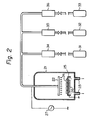
- the present invention will now be illustrated by explaining the formation of the silicon oxynitride film by the plasma CVD method.
- the plasuma CVD apparatus comprises a bell jar type reactive chamber 21 so made of quartz and an electrode 22 having a number of holes for discharging a gas.
- the electrode 22 communicates with a container 31 containing monosilane (SiH ), a container 32 containing ammonia (NH 3 ) and a container 33 containing nitrous oxide (N 2 0) through flow controllers, 34, 35 and 36, respectively.
- the reactive chamber 21 has exhaust ports 23 at the bottom thereof.
- a plurality of silicon substrates 24 are placed on a base 25 which also serves as an electrode is heated by means of a heater 26 provided below the base 25.
- a high frequency power supply is denoted by 27.
- the reactive chamber is evacuated until ⁇ the pressure therein reaches 5 x 10 -3 Torr. Then, a gaseous mixture consisting of monosilane (SiH 4 ), ammonia (NH 3 ) or nitrogen (N 2 ) and nitrous oxide (N 2 0) is introduced into the reactive chamber 21.
- the temperature within the reactive chamber is maintained at 350°C by means of the heater 26.
- a high frequency output (frequency: 13.56 MHz, power: 10 W corresponding to 0.1 w/cm 2 of the electrode surface) is applied between the electrode 22 and the base 25 by means of the high frequency power supply 27.
- the pressure within the reactive chamber may vary within the range of from 0.3 to 2.0 Torr.
- the temperature within the reactive chamber may vary within the range of from 250 to 450°C.
- the output of the high frequency power supply is varied, the growth rate of the silicon oxynitride film to be deposited on the silicon substrates 24 is changed and the composition of the resultant film is also changed to some degree.
- pure oxygen is used as the source of oxygen, the oxygen starts to react with the other reactive gases at the junction of these gases before the oxygen reaches the surrounding of the silicon substrates 24. Therefore, the use of pure oxygen is not favourable.
- a silicon oxynitride film is deposited on the silicon substrates 24 by varying the ratio of NH 3 to N 2 0 while maintaining the temperature within the reactive chamber, the pressure within the reactive chamber and the flow ratio of (NH 3 + H 2 0) to SiH 4 in the gaseous mixture at constant values of 350°C, 1.0 Torr and 10, respectively.
- the properties of the resultant silicon oxynitride films are shown in Fig. 3 and Table 1 and 2.
- Rox represents an introduction ratio by volume of N 2 0 which is defined by the formula: N 2 0/(NH 3 + N 2 0), ⁇ a represents an absorption edge which is defined by a wave length of ultraviolet rays exhibiting a 10% transmission through a 1 (pm) thick film.
- Table 1 shows a shift in the absorption edge Xa (A) of the resultant silicon oxynitride when the Rox is varied within the range of from 0 to 0.5.
- a one micron thick aluminum wiring was formed on an insulating layer which covered a silicon substrate.
- a . o 7000 A thick silicon oxynitride film was deposited on the aluminum wiring. The resistance to cracking of this oxynitride film was investigated.
- Table 2 shows a relationship between the Rox and the resistance to cracking of the resultant film.
- the resistance to cracking was determined by heat treating the resultant film in an atmosphere consisting of 3% by volume of H 2 and the remainder of N 2 , at a temperature of 450°C, for 30 minutes.
- the mark o indicates no generation of cracks
- the mark x indicates the generation of cracks.
- the cracks occur in the form of a plurality of radial mustaches at a portion of the surface passivation film under which the extension of the underlaid wire is turned at an angle of 90°. It is considered that this occurrence of cracks is ascribable to a strain which is in a relatively high tensile stress state in the silicon nitride film. Oxygen is effective for reducing this strain in the silicon nitride film.
- the composition of the resulting film approaches silicon dioxide which exhibits a poor moisture proofness.
- the poor moisture proofness is, however, negligible, when the oxygen concentration is 70% or lower.
- the intensity of the light transmitted through the substrate is plotted versus the wave length of the infrared rays.
- the silicon oxynitride have an oxygen concentration of from 20 to 70%, i.e. it is prepared at a Rox value of from 0.1 to 0.5, and in terms of an absorption wave length, it exhibits a Xa of from 1900 0 to 2300 A.
- the silicon oxynitride may be deposited by an atmospheric CVD method or a reduced pressure CVD method using a pressure of from 1 to 3 Torr. In this case, the deposition operation may be carried out under the same conditions as those used in the case of the plasma CVD method, except that instead of using the high frequency electric source, the interior of the reactive chamber is heated to a temperature of from 700 to 800°C.
- a high melting point metal such as titanium
- ions are sputtered toward a silicon target in an atmosphere consisting of argon (Ar), ammonia (NH3) and oxygen (0 2 ) in the reactive chamber.
- Ar argon
- NH3 ammonia
- oxygen (0 2 )
- the silicon nitride film according to the present invention is very suitable as a surface passivation film for the EPROM device whose information memorized thereon is erased by ultraviolet rays.
Landscapes
- Chemical & Material Sciences (AREA)
- Inorganic Chemistry (AREA)
- General Chemical & Material Sciences (AREA)
- Chemical Kinetics & Catalysis (AREA)
- Engineering & Computer Science (AREA)
- Materials Engineering (AREA)
- Mechanical Engineering (AREA)
- Metallurgy (AREA)
- Organic Chemistry (AREA)
- Formation Of Insulating Films (AREA)
- Read Only Memory (AREA)
- Non-Volatile Memory (AREA)
Applications Claiming Priority (2)
| Application Number | Priority Date | Filing Date | Title |
|---|---|---|---|
| JP11827879A JPS5642377A (en) | 1979-09-14 | 1979-09-14 | Ultraviolet ray erasable type rewritable read-only memory |
| JP118278/79 | 1979-09-14 |
Publications (3)
| Publication Number | Publication Date |
|---|---|
| EP0025717A2 true EP0025717A2 (fr) | 1981-03-25 |
| EP0025717A3 EP0025717A3 (en) | 1983-04-06 |
| EP0025717B1 EP0025717B1 (fr) | 1986-12-10 |
Family
ID=14732691
Family Applications (1)
| Application Number | Title | Priority Date | Filing Date |
|---|---|---|---|
| EP80303242A Expired EP0025717B1 (fr) | 1979-09-14 | 1980-09-15 | Dispositif semiconducteur comprenant deux couches isolantes et procédé pour le fabriquer |
Country Status (4)
| Country | Link |
|---|---|
| US (2) | US4532022A (fr) |
| EP (1) | EP0025717B1 (fr) |
| JP (1) | JPS5642377A (fr) |
| DE (1) | DE3071862D1 (fr) |
Cited By (8)
| Publication number | Priority date | Publication date | Assignee | Title |
|---|---|---|---|---|
| EP0032024A3 (en) * | 1979-12-26 | 1984-06-13 | Fujitsu Limited | Process for producing semiconductor devices, devices produced by the process, and circuits and articles including such devices |
| US4620986A (en) * | 1984-11-09 | 1986-11-04 | Intel Corporation | MOS rear end processing |
| EP0180219A3 (fr) * | 1984-11-01 | 1986-12-17 | Nec Corporation | Unité d'empaquetage de circuit intégré et condensateur incorporé et procédé pour sa fabrication |
| EP0259826A1 (fr) * | 1986-09-08 | 1988-03-16 | Nec Corporation | Composant semi-conducteur ayant un film d'oxynitrure de silicium à résistance à l'humidité améliorée |
| EP0280276A3 (en) * | 1987-02-27 | 1989-04-26 | Kabushiki Kaisha Toshiba | Ultraviolet erasable nonvolatile semiconductor memory deultraviolet erasable nonvolatile semiconductor memory device and manufacturing method therefor vice and manufacturing method therefor |
| EP0281324A3 (fr) * | 1987-03-04 | 1989-10-18 | Advanced Micro Devices, Inc. | Structure de passivation pour structures de circuits intégrés |
| EP0408054A3 (en) * | 1989-07-14 | 1991-10-30 | Kabushiki Kaisha Toshiba | Ultraviolet erasable non-volatile semiconductor memory apparatus |
| EP1191819A3 (fr) * | 2000-09-25 | 2005-09-28 | Pioneer Corporation | Panneau d'affichage électroluminescent |
Families Citing this family (58)
| Publication number | Priority date | Publication date | Assignee | Title |
|---|---|---|---|---|
| JPS58219748A (ja) * | 1982-06-15 | 1983-12-21 | Toshiba Corp | 半導体装置 |
| JPS596370A (ja) * | 1982-06-29 | 1984-01-13 | Fujitsu Ltd | 高融点金属窒化膜の形成方法 |
| USRE34535E (en) * | 1983-02-23 | 1994-02-08 | Texas Instruments Incorporated | Floating gate memory with improved dielectric |
| US4697330A (en) * | 1983-02-23 | 1987-10-06 | Texas Instruments Incorporated | Floating gate memory process with improved dielectric |
| JPS6039837A (ja) * | 1983-08-12 | 1985-03-01 | Nec Corp | 絶縁膜の成長方法 |
| US6784033B1 (en) | 1984-02-15 | 2004-08-31 | Semiconductor Energy Laboratory Co., Ltd. | Method for the manufacture of an insulated gate field effect semiconductor device |
| JPS6195534A (ja) * | 1984-10-17 | 1986-05-14 | Hitachi Ltd | 半導体記憶装置 |
| JPH0752718B2 (ja) * | 1984-11-26 | 1995-06-05 | 株式会社半導体エネルギー研究所 | 薄膜形成方法 |
| US6786997B1 (en) | 1984-11-26 | 2004-09-07 | Semiconductor Energy Laboratory Co., Ltd. | Plasma processing apparatus |
| US4665426A (en) * | 1985-02-01 | 1987-05-12 | Advanced Micro Devices, Inc. | EPROM with ultraviolet radiation transparent silicon nitride passivation layer |
| US6673722B1 (en) | 1985-10-14 | 2004-01-06 | Semiconductor Energy Laboratory Co., Ltd. | Microwave enhanced CVD system under magnetic field |
| US6230650B1 (en) | 1985-10-14 | 2001-05-15 | Semiconductor Energy Laboratory Co., Ltd. | Microwave enhanced CVD system under magnetic field |
| US4717631A (en) * | 1986-01-16 | 1988-01-05 | Rca Corporation | Silicon oxynitride passivated semiconductor body and method of making same |
| JPS62172733A (ja) * | 1986-01-16 | 1987-07-29 | ア−ルシ−エ− コ−ポレ−ション | 半導体基体 |
| US4825271A (en) * | 1986-05-20 | 1989-04-25 | Kabushiki Kaisha Toshiba | Nonvolatile semiconductor memory |
| US4758869A (en) * | 1986-08-29 | 1988-07-19 | Waferscale Integration, Inc. | Nonvolatile floating gate transistor structure |
| US5034786A (en) * | 1986-08-29 | 1991-07-23 | Waferscale Integration, Inc. | Opaque cover for preventing erasure of an EPROM |
| US5427824A (en) * | 1986-09-09 | 1995-06-27 | Semiconductor Energy Laboratory Co., Ltd. | CVD apparatus |
| KR910003742B1 (ko) * | 1986-09-09 | 1991-06-10 | 세미콘덕터 에너지 라보라터리 캄파니 리미티드 | Cvd장치 |
| US5010024A (en) * | 1987-03-04 | 1991-04-23 | Advanced Micro Devices, Inc. | Passivation for integrated circuit structures |
| JPS63316476A (ja) * | 1987-06-18 | 1988-12-23 | Seiko Instr & Electronics Ltd | 半導体装置およびその製造方法 |
| JPH021988A (ja) * | 1987-12-03 | 1990-01-08 | Texas Instr Inc <Ti> | 電気的にプログラム可能なメモリ・セル |
| EP0346055B1 (fr) * | 1988-06-06 | 1995-04-19 | Research Development Corporation Of Japan | Procédé pour provoquer une réaction dans le plasma sous pression atmosphérique |
| US5013692A (en) * | 1988-12-08 | 1991-05-07 | Sharp Kabushiki Kaisha | Process for preparing a silicon nitride insulating film for semiconductor memory device |
| US5107323A (en) * | 1988-12-22 | 1992-04-21 | At&T Bell Laboratories | Protective layer for high voltage devices |
| US4982250A (en) * | 1989-01-04 | 1991-01-01 | Motorola, Inc. | Mosture barrier for floating gate transistors |
| DE4013306A1 (de) * | 1990-04-26 | 1991-10-31 | Hoechst Ag | Optische formkoerper aus siliziumnitrid, sowie verfahren zu deren herstellung |
| JP2814009B2 (ja) * | 1990-06-05 | 1998-10-22 | 三菱電機株式会社 | 半導体装置の製造方法 |
| JP3197557B2 (ja) * | 1990-11-27 | 2001-08-13 | 株式会社半導体エネルギー研究所 | 被膜形成方法 |
| JP2667605B2 (ja) * | 1991-02-21 | 1997-10-27 | 株式会社東芝 | 不揮発性半導体記憶装置およびその製造方法 |
| US5260236A (en) * | 1991-06-07 | 1993-11-09 | Intel Corporation | UV transparent oxynitride deposition in single wafer PECVD system |
| EP0617461B1 (fr) * | 1993-03-24 | 1997-09-10 | AT&T Corp. | Procédé pour la formation de couches diélectriques oxynitrides lors de la fabrication de circuits intégrés |
| DE4333160A1 (de) * | 1993-09-29 | 1995-03-30 | Siemens Ag | Herstellverfahren für eine nitridierte Siliziumoxidschicht mit verringerter Temperaturbelastung |
| US5397720A (en) * | 1994-01-07 | 1995-03-14 | The Regents Of The University Of Texas System | Method of making MOS transistor having improved oxynitride dielectric |
| US5478765A (en) * | 1994-05-04 | 1995-12-26 | Regents Of The University Of Texas System | Method of making an ultra thin dielectric for electronic devices |
| JP3632256B2 (ja) * | 1994-09-30 | 2005-03-23 | 株式会社デンソー | 窒化シリコン膜を有する半導体装置の製造方法 |
| JPH09511622A (ja) * | 1994-11-07 | 1997-11-18 | マクロニクス インターナショナル カンパニー リミテッド | 集積回路表面保護方法および構造 |
| US5801076A (en) * | 1995-02-21 | 1998-09-01 | Advanced Micro Devices, Inc. | Method of making non-volatile memory device having a floating gate with enhanced charge retention |
| US5541141A (en) * | 1995-02-27 | 1996-07-30 | Hyundai Electronics Industries Co., Ltd. | Method for forming an oxynitride film in a semiconductor device |
| DE19507130C2 (de) * | 1995-03-01 | 1997-08-21 | Daimler Benz Ag | Passivierung von SiC-Bauelementen |
| US6022799A (en) * | 1995-06-07 | 2000-02-08 | Advanced Micro Devices, Inc. | Methods for making a semiconductor device with improved hot carrier lifetime |
| US5710067A (en) * | 1995-06-07 | 1998-01-20 | Advanced Micro Devices, Inc. | Silicon oxime film |
| US6103555A (en) * | 1996-06-10 | 2000-08-15 | Integrated Device Technology, Inc. | Method of improving the reliability of low-voltage programmable antifuse |
| US6121133A (en) | 1997-08-22 | 2000-09-19 | Micron Technology, Inc. | Isolation using an antireflective coating |
| US6294459B1 (en) | 1998-09-03 | 2001-09-25 | Micron Technology, Inc. | Anti-reflective coatings and methods for forming and using same |
| US6458512B1 (en) | 1998-10-13 | 2002-10-01 | 3M Innovative Properties Company | Oxynitride encapsulated electroluminescent phosphor particles |
| JP2001068658A (ja) * | 1999-08-27 | 2001-03-16 | Sony Corp | 固体撮像装置及びその製造方法 |
| US6559007B1 (en) * | 2000-04-06 | 2003-05-06 | Micron Technology, Inc. | Method for forming flash memory device having a tunnel dielectric comprising nitrided oxide |
| US6451713B1 (en) * | 2000-04-17 | 2002-09-17 | Mattson Technology, Inc. | UV pretreatment process for ultra-thin oxynitride formation |
| JP5068402B2 (ja) * | 2000-12-28 | 2012-11-07 | 公益財団法人国際科学振興財団 | 誘電体膜およびその形成方法、半導体装置、不揮発性半導体メモリ装置、および半導体装置の製造方法 |
| ATE533177T1 (de) * | 2001-09-17 | 2011-11-15 | Advion Biosystems Inc | Dielektrischer film |
| US6909162B2 (en) * | 2001-11-02 | 2005-06-21 | Omnivision Technologies, Inc. | Surface passivation to reduce dark current in a CMOS image sensor |
| US6462365B1 (en) * | 2001-11-06 | 2002-10-08 | Omnivision Technologies, Inc. | Active pixel having reduced dark current in a CMOS image sensor |
| US6706643B2 (en) | 2002-01-08 | 2004-03-16 | Mattson Technology, Inc. | UV-enhanced oxy-nitridation of semiconductor substrates |
| JP4340416B2 (ja) * | 2002-02-26 | 2009-10-07 | Spansion Japan株式会社 | 半導体記憶装置の製造方法 |
| US20090071371A1 (en) * | 2007-09-18 | 2009-03-19 | College Of William And Mary | Silicon Oxynitride Coating Compositions |
| US20100178758A1 (en) * | 2009-01-15 | 2010-07-15 | Macronix International Co., Ltd. | Methods for fabricating dielectric layer and non-volatile memory |
| US11302827B2 (en) * | 2020-01-23 | 2022-04-12 | Nanya Technology Corp. | Semiconductor device with sidewall oxidized dielectric and method for fabricating the same |
Family Cites Families (10)
| Publication number | Priority date | Publication date | Assignee | Title |
|---|---|---|---|---|
| US3607697A (en) * | 1968-04-18 | 1971-09-21 | Sprague Electric Co | Sputtering process for making a film of silica and silicon nitride |
| US3629088A (en) * | 1968-07-11 | 1971-12-21 | Sperry Rand Corp | Sputtering method for deposition of silicon oxynitride |
| US3652324A (en) * | 1968-08-15 | 1972-03-28 | Westinghouse Electric Corp | A METHOD OF VAPOR DEPOSITING A LAYER OF Si{11 N{11 {0 ON A SILICON BASE |
| US3883889A (en) * | 1974-04-15 | 1975-05-13 | Micro Power Systems Inc | Silicon-oxygen-nitrogen layers for semiconductor devices |
| US3976524A (en) * | 1974-06-17 | 1976-08-24 | Ibm Corporation | Planarization of integrated circuit surfaces through selective photoresist masking |
| US4091406A (en) * | 1976-11-01 | 1978-05-23 | Rca Corporation | Combination glass/low temperature deposited Siw Nx Hy O.sub.z |
| IT1088852B (it) * | 1976-11-01 | 1985-06-10 | Rca Corp | Struttura passivante per un dispositivo simeconduttore |
| DE2832388C2 (de) * | 1978-07-24 | 1986-08-14 | Siemens Ag, 1000 Berlin Und 8000 Muenchen | Verfahren zum Herstellen von MNOS- und MOS-Transistoren in Silizium-Gate-Technologie auf einem Halbleitersubstrat |
| US4229755A (en) * | 1978-08-15 | 1980-10-21 | Rockwell International Corporation | Fabrication of very large scale integrated circuits containing N-channel silicon gate nonvolatile memory elements |
| US4253881A (en) * | 1978-10-23 | 1981-03-03 | Rudolf Hezel | Solar cells composed of semiconductive materials |
-
1979
- 1979-09-14 JP JP11827879A patent/JPS5642377A/ja active Granted
-
1980
- 1980-09-15 DE DE8080303242T patent/DE3071862D1/de not_active Expired
- 1980-09-15 EP EP80303242A patent/EP0025717B1/fr not_active Expired
-
1983
- 1983-05-31 US US06/499,477 patent/US4532022A/en not_active Expired - Lifetime
-
1984
- 1984-02-13 US US06/578,992 patent/US4581622A/en not_active Expired - Lifetime
Cited By (8)
| Publication number | Priority date | Publication date | Assignee | Title |
|---|---|---|---|---|
| EP0032024A3 (en) * | 1979-12-26 | 1984-06-13 | Fujitsu Limited | Process for producing semiconductor devices, devices produced by the process, and circuits and articles including such devices |
| EP0180219A3 (fr) * | 1984-11-01 | 1986-12-17 | Nec Corporation | Unité d'empaquetage de circuit intégré et condensateur incorporé et procédé pour sa fabrication |
| US4620986A (en) * | 1984-11-09 | 1986-11-04 | Intel Corporation | MOS rear end processing |
| EP0259826A1 (fr) * | 1986-09-08 | 1988-03-16 | Nec Corporation | Composant semi-conducteur ayant un film d'oxynitrure de silicium à résistance à l'humidité améliorée |
| EP0280276A3 (en) * | 1987-02-27 | 1989-04-26 | Kabushiki Kaisha Toshiba | Ultraviolet erasable nonvolatile semiconductor memory deultraviolet erasable nonvolatile semiconductor memory device and manufacturing method therefor vice and manufacturing method therefor |
| EP0281324A3 (fr) * | 1987-03-04 | 1989-10-18 | Advanced Micro Devices, Inc. | Structure de passivation pour structures de circuits intégrés |
| EP0408054A3 (en) * | 1989-07-14 | 1991-10-30 | Kabushiki Kaisha Toshiba | Ultraviolet erasable non-volatile semiconductor memory apparatus |
| EP1191819A3 (fr) * | 2000-09-25 | 2005-09-28 | Pioneer Corporation | Panneau d'affichage électroluminescent |
Also Published As
| Publication number | Publication date |
|---|---|
| JPS5642377A (en) | 1981-04-20 |
| EP0025717A3 (en) | 1983-04-06 |
| US4532022A (en) | 1985-07-30 |
| JPS5649471B2 (fr) | 1981-11-21 |
| DE3071862D1 (en) | 1987-01-22 |
| EP0025717B1 (fr) | 1986-12-10 |
| US4581622A (en) | 1986-04-08 |
Similar Documents
| Publication | Publication Date | Title |
|---|---|---|
| EP0025717B1 (fr) | Dispositif semiconducteur comprenant deux couches isolantes et procédé pour le fabriquer | |
| EP0380326B1 (fr) | Procédé de fabrication d'un dispositif à semi-conducteur | |
| US6048766A (en) | Flash memory device having high permittivity stacked dielectric and fabrication thereof | |
| EP0186443B1 (fr) | Films de nitrure de silicium pour circuits intégrés | |
| EP1340247B1 (fr) | Procede de formation de films dielectriques | |
| US5525550A (en) | Process for forming thin films by plasma CVD for use in the production of semiconductor devices | |
| EP0572704B1 (fr) | Procédé de fabrication d'un dispositif semi-conducteur comportant une méthode de réforme d'une couche isolante obtenue par CVD à basse température | |
| US5866932A (en) | Insulating film formed using an organic silane and method of producing semiconductor device | |
| US4588610A (en) | Photo-chemical vapor deposition of silicon nitride film | |
| US6924241B2 (en) | Method of making a silicon nitride film that is transmissive to ultraviolet light | |
| JPH09307074A (ja) | 誘電体容量素子を用いた記憶装置及び製造方法 | |
| JP4003846B2 (ja) | 半導体装置のキャパシタ製造方法 | |
| US6906365B2 (en) | Ferroelectric memory device including an upper protection electrode | |
| KR100391485B1 (ko) | 강유전체막을사용한장치의제조방법및장치 | |
| US5001527A (en) | Semiconductor device with thin insulation film | |
| CA2053419A1 (fr) | Methode d'obtention par d.c.p.v. d'une pellicule d'oxynitrure de silicium | |
| KR20030041088A (ko) | 유전체 박막 제조 방법 및 시스템 | |
| JPH09181071A (ja) | Bpsg膜の表面平坦化方法 | |
| JPH08125197A (ja) | 半導体装置の作製方法および半導体装置の作製装置 | |
| KR20010088207A (ko) | 탄탈륨산화막-티타늄산화막 복합유전막 형성방법 | |
| US6709927B1 (en) | Process for treating ONO dielectric film of a floating gate memory cell | |
| JPH06330322A (ja) | 絶縁膜の作製方法 | |
| JPH03276723A (ja) | 絶縁薄膜およびその形成方法 | |
| Wang et al. | Investigation of a high quality and ultraviolet-light transparent plasma-enhanced chemical vapor deposition silicon nitride film for non-volatile memory application | |
| KR100274353B1 (ko) | 반도체소자의캐패시터제조방법 |
Legal Events
| Date | Code | Title | Description |
|---|---|---|---|
| PUAI | Public reference made under article 153(3) epc to a published international application that has entered the european phase |
Free format text: ORIGINAL CODE: 0009012 |
|
| 17P | Request for examination filed |
Effective date: 19800919 |
|
| AK | Designated contracting states |
Designated state(s): DE FR GB NL |
|
| PUAL | Search report despatched |
Free format text: ORIGINAL CODE: 0009013 |
|
| AK | Designated contracting states |
Designated state(s): DE FR GB NL |
|
| GRAA | (expected) grant |
Free format text: ORIGINAL CODE: 0009210 |
|
| AK | Designated contracting states |
Kind code of ref document: B1 Designated state(s): DE FR GB NL |
|
| PG25 | Lapsed in a contracting state [announced via postgrant information from national office to epo] |
Ref country code: NL Effective date: 19861210 |
|
| ET | Fr: translation filed | ||
| REF | Corresponds to: |
Ref document number: 3071862 Country of ref document: DE Date of ref document: 19870122 |
|
| NLV1 | Nl: lapsed or annulled due to failure to fulfill the requirements of art. 29p and 29m of the patents act | ||
| PLBE | No opposition filed within time limit |
Free format text: ORIGINAL CODE: 0009261 |
|
| STAA | Information on the status of an ep patent application or granted ep patent |
Free format text: STATUS: NO OPPOSITION FILED WITHIN TIME LIMIT |
|
| 26N | No opposition filed | ||
| PGFP | Annual fee paid to national office [announced via postgrant information from national office to epo] |
Ref country code: GB Payment date: 19930907 Year of fee payment: 14 |
|
| PG25 | Lapsed in a contracting state [announced via postgrant information from national office to epo] |
Ref country code: GB Effective date: 19940915 |
|
| GBPC | Gb: european patent ceased through non-payment of renewal fee |
Effective date: 19940915 |
|
| PGFP | Annual fee paid to national office [announced via postgrant information from national office to epo] |
Ref country code: FR Payment date: 19990909 Year of fee payment: 20 |
|
| PGFP | Annual fee paid to national office [announced via postgrant information from national office to epo] |
Ref country code: DE Payment date: 19990927 Year of fee payment: 20 |