EP0029228A2 - Laser-Halbleitervorrichtung - Google Patents
Laser-Halbleitervorrichtung Download PDFInfo
- Publication number
- EP0029228A2 EP0029228A2 EP80107031A EP80107031A EP0029228A2 EP 0029228 A2 EP0029228 A2 EP 0029228A2 EP 80107031 A EP80107031 A EP 80107031A EP 80107031 A EP80107031 A EP 80107031A EP 0029228 A2 EP0029228 A2 EP 0029228A2
- Authority
- EP
- European Patent Office
- Prior art keywords
- semiconductor
- current
- region
- laser oscillation
- switching means
- Prior art date
- Legal status (The legal status is an assumption and is not a legal conclusion. Google has not performed a legal analysis and makes no representation as to the accuracy of the status listed.)
- Granted
Links
Images




Classifications
-
- H—ELECTRICITY
- H01—ELECTRIC ELEMENTS
- H01S—DEVICES USING THE PROCESS OF LIGHT AMPLIFICATION BY STIMULATED EMISSION OF RADIATION [LASER] TO AMPLIFY OR GENERATE LIGHT; DEVICES USING STIMULATED EMISSION OF ELECTROMAGNETIC RADIATION IN WAVE RANGES OTHER THAN OPTICAL
- H01S5/00—Semiconductor lasers
- H01S5/06—Arrangements for controlling the laser output parameters, e.g. by operating on the active medium
- H01S5/062—Arrangements for controlling the laser output parameters, e.g. by operating on the active medium by varying the potential of the electrodes
- H01S5/0625—Arrangements for controlling the laser output parameters, e.g. by operating on the active medium by varying the potential of the electrodes in multi-section lasers
-
- H—ELECTRICITY
- H01—ELECTRIC ELEMENTS
- H01S—DEVICES USING THE PROCESS OF LIGHT AMPLIFICATION BY STIMULATED EMISSION OF RADIATION [LASER] TO AMPLIFY OR GENERATE LIGHT; DEVICES USING STIMULATED EMISSION OF ELECTROMAGNETIC RADIATION IN WAVE RANGES OTHER THAN OPTICAL
- H01S5/00—Semiconductor lasers
- H01S5/02—Structural details or components not essential to laser action
- H01S5/026—Monolithically integrated components, e.g. waveguides, monitoring photo-detectors, drivers
- H01S5/0261—Non-optical elements, e.g. laser driver components, heaters
-
- H—ELECTRICITY
- H01—ELECTRIC ELEMENTS
- H01S—DEVICES USING THE PROCESS OF LIGHT AMPLIFICATION BY STIMULATED EMISSION OF RADIATION [LASER] TO AMPLIFY OR GENERATE LIGHT; DEVICES USING STIMULATED EMISSION OF ELECTROMAGNETIC RADIATION IN WAVE RANGES OTHER THAN OPTICAL
- H01S5/00—Semiconductor lasers
- H01S5/06—Arrangements for controlling the laser output parameters, e.g. by operating on the active medium
- H01S5/062—Arrangements for controlling the laser output parameters, e.g. by operating on the active medium by varying the potential of the electrodes
- H01S5/06209—Arrangements for controlling the laser output parameters, e.g. by operating on the active medium by varying the potential of the electrodes in single-section lasers
- H01S5/06213—Amplitude modulation
Definitions
- This invention relates to a semiconductor light emitting device of a novel structure wherein the modulation of a semiconductor laser element is effected with transistors which are integrated and disposed onthe same substrate as that of the semiconductor laser.
- a semiconductor laser element provides a wide application in, for example, optical communication systems such as data bus or computer-link since it is small in size and capable of performing rapid modulation.
- the modulation of a semiconductor laser element is usually performed in such a manner as described below.
- a direct current is sent through a circuit element called a bias-T unit, consisting of a capacitor and a coil, from the side of the coil; the excitation concentration is raised up to near the laser oscillation threshold; and the laser output light is modulated through the superposition of a current pulse of 30 to 70 mA sent from the side of the capacitor.
- a bias-T unit consisting of a capacitor and a coil, from the side of the coil
- the excitation concentration is raised up to near the laser oscillation threshold
- the laser output light is modulated through the superposition of a current pulse of 30 to 70 mA sent from the side of the capacitor.
- Such apparatus have been put on the market.
- a high speed modulation of 1 to 2 GJits/sec. it is difficult for ordinary silicon transistors to generate current pulses suitable for the high speed modulation.
- the bias-T unit is very voluminous in comparison with the laser element and the size of a
- a semiconductor light emitting device of this invention comprises a layered semiconductor region capable of laser oscillation, and at least two sets of switching elements, one of which constructs means for supplying a current near a laser oscillation threshold value to the layered semiconductor region for the laser oscillation and the other of which constructs means for modulating the laser beam on the basis of an external input thereof.
- the switching elements are formed of field-effect transistors (hereinbelow, abbreviated to "FETs").
- FETs field-effect transistors
- the sources (or drains) of the two FETs are short-circuited, and the node is connected to one electrode of the layered semiconductor region causing the laser oscillation. Further, the drains (or sources) of the two FETs are short-circuited, and the node is used as a part for an external input.
- a composite or combined semiconductor light emitting device which consists of a semiconductor laser and switching elements and which is compact can be provided.
- the composite semiconductor light emitting device can perform modulation up to a high frequency region directly.
- the yield or available percentage in manufacture can be sharply increased.
- GaAs FET GaAs field-effect transistor
- Figure 1 shows an equivalent circuit of this semiconductor light emitting device.
- numeral 1 designates a semiconductor laser element, numeral 2 an FET, and numeral 3 a gate electrode.
- Figure 2 shows an equivalent circuit of a semiconductor light emitting device of the same sort.
- numeral 1 indicates a semiconductor laser element, numeral 2 an FET, and numeral 3 a gate electrode.
- a D.C. voltage V D is applied to the monolithically integrated device and a modulating signal to the gate of the FET.
- I 1 denote a current which flows in the absence of the gate signal (during the zero bias)
- ⁇ I denote a current which is suppressed by the pulse applied to the gate.
- the value of (I 1 - ⁇ I) becomes approximately equal to or somewhat greater than the oscillation threshold current I th of the laser element. In this case, the modulation factor of the laser power is great, the period of time in which the laser element rises for the oscillation becomes the shortest, and no phase lag occurs.
- This invention contemplates to provide a composite semiconductor light emitting device which solves the problem of the yield and further facilitates handling as a light source for high-speed modulation.
- Figure 5 shows an equivalent circuit of a semiconductor light emitting device of this invention. At least two FETs (4, 5) whose gate input terminals (6, 7) are independent of each other, and a semiconductor laser element 1 are integrated in combination.
- the FETs may well be quite identical to each other, or may well differ in performance.
- a D.C. bias is applied to one FET (4), to regulate a source - drain current 1 1 to be approximately equal to a laser oscillation threshold value I th .
- a modulating signal is applied to the gate of the other FET (5). Then, a current I 2 which flows during the zero bias decreases ⁇ I, and a laser beam can be modulated.
- Figure 6 illustrates the relationship among the source - drain currents 1 1 and I 2 and the decrement ⁇ I. It is very easy to set the range of AI in the rectilinear part of a current - output power characteristic curve. With this system, it is possible to modulate a laser element of an arbitrary threshold value at a desired laser intensity.
- the semiconductor light emitting device of this invention shall be shortly termed "TC laser" by taking the first letters of the words of "Threshold Control".
- Figures 7 and 8 show a plan view and a sectional view of a typical semiconductor light emitting device of this invention, respectively.
- the sectional view is taken along A - A in the plan view of Figure 7.
- first, second and third semiconductor layers 22, 23 and 24 which constitute a semiconductor laser element.
- the stacked region of a fifth semiconductor layer 26 which forms the channel of an FET portion is formed through, at least, a fourth semiconductor layer 25 having a high resistivity.
- the first semiconductor layer 22 serves as a first clad layer of the semiconductor laser element, the second semiconductor layer'23 as an active layer thereof, and the third semiconductor layer 24 as a second clad layer thereof.
- the first and third semiconductor layers are relatively low in the refractive index as compared with the second semiconductor layer, and they have conductivity types opposite to each other. Further, the first and third semiconductor layers are relatively great in the forbidden band gap.
- the fourth semiconductor layer needs to have a resistivity of at least 10 ⁇ cm, and a range of resistivities up to 100 ⁇ cm - 1 k ⁇ cm or so is employed in practical use. This layer is necessary for isolating the semiconductor laser element portion and the FET portion.
- a recess or groove 27 is for isolation.It is not always necessary, depending upon the design of the semiconductor laser element and the FETs, but more favorably they are insulated.
- the insulating expedient of putting an inorganic insulator such as Si0 2 , or a resin or the like into the recess may be employed as well.
- a high-resistivity region can also be formed by, e.g. implanting protons into a predetermined part without digging the recess.
- the isolation may well be resorted to such insulating expedient. As to such isolation, techniques used in the fields of conventional semiconductor lasers and semiconductor devices may be employed.
- this semiconductor light emitting device is to be constructed of a GaAs-GaAlAs-based material
- the respective semiconductor layers are, in general, selected as follows:
- the second FET is fabricated by a similar structure. Sections orthogonal to the traveling direction of a laser beam are formed with reflective faces by, for example, cleavage. Thus, an optical resonator is constructed.
- the semiconductor light emitting device of the construction as above described can be caused to perform laser oscillation by short-circuiting the electrodes 38 and 36 and applying a voltage across the electrodes 35 and 40.
- Numeral 39 designates a lead for short-circuiting the electrodes 38 and 36. Due to the way of taking the section, however, it is illustrated in a split manner in the drawing.
- the oscillation of the semiconductor laser can be controlled by applying a control voltage to a gate electrode 10.
- the semiconductor layers in Figure 8 the first to fifth semiconductor layers are successively stacked, and the semiconductor laser element and the FET portion are respectively constructed in the desired regions. With this structure, the manufacturing method is easy.
- the semiconductor light emitting device of this invention is not restricted to such fashion of stacking the semiconductor layers.
- it is of course allowed that the stacked structure of the first, second and third semiconductor layers constituting the semiconductor laser element and the stacked structure of the fourth and fifth semiconductor - layers constituting the FET portion are separately grown on the semiconductor substrate for growth.
- Such different practical constructions of this invention will be concretely described in conjunction with examples.
- the construction of the semiconductor laser for optical confinement, the method of emitting light, etc. are not restricted to those of the foregoing embodiment.
- this invention is not restricted to semiconductor materials to be referred to in the examples. While there are various expedients for the mode stabilization of semiconductor lasers, they may of course be applied to the semiconductor laser portion of the light emitting semiconductor device of this invention, and they fall within the scope of this invention.
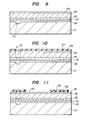
- Figures 9 to 14 are sectional views of a device showing various steps of a process for manufacturing the semiconductor light emitting device of this invention.
- a stripe-shaped recess 50 was formed in the surface of an n-type GaAs substrate (electron density n ⁇ 10 18 /cm3) 21 having the (100) plane as its upper surface.
- respective layers to be described below were formed by the well-known liquid epitaxial growth employing a slide boat.
- the aforecited recess may be formed by the selective etching or the like so as to extend in the direction perpendicular to the reflective faces of a resonator.
- the semiconductor layers having flat surfaces can be readily formed on the semiconductor substrate having an unevenness on the order of several ⁇ m by the liquid epitaxial growth.
- the recess serves to control a transverse mode by exploiting the leakage or penetration of laser radiation into the substrate.
- Techniques for the optical confinement have been reported in detail in "IEEE J. Quantum Electron", QE-14, 89 (1978) by K. Aiki et al., etc.
- an n-type Ga 0.7 Al 0.3 As layer (n N 5 x 10 17 /cm 3 ) was made 2 ⁇ m thick; as a second semiconductor layer 23, an n-type GaAs layer (n ⁇ 1 0 16 /cm 3 ) was made 0.1 ⁇ m thick; as a third semiconductor layer 2 4, a p- type Ga 0.7 Al 0.3 As layer (hole density p ⁇ 5 x 10 17 / cm 3 ) was made 1 ⁇ m thick; as a fourth semiconductor layer 25, a p - type Ga 0.7 Al 0.3 As layer (p ⁇ 1 x 10 14 /cm 3 , resistivity ⁇ 600 ⁇ cm) was made 1 ⁇ m thick; and as a fifth semiconductor layer 26, an n-type GaAs layer (n ⁇ 2 x 10 17 /cm 3 ) was made 0.3 ⁇ m thick.
- a two-layered insulating film consisting of Al 2 0 3 at a thickness of 0.2 ⁇ m and SiO 2 at a thickness of 0.3 ⁇ m was formed by the well-known CVD (Chemical Vapor Deposition) process. That part of the two-layered insulating film which corresponded to an electrode lead-out portion of a semiconductor laser element was opened to a width of 6 ⁇ m.
- Liquid etchants were a mixed solution consisting of hydrogen fluoride and ammonium fluoride (at 1 : 6, for Si0 2 ) and phosphoric acid (for Al 2 O 3 ).
- the SiO 2 -Al 2 O 3 two-layered film became a mask for selective diffusion 27. Through the opening, Zn was diffused at a width of 6 ⁇ m and a depth down to the third semiconductor layer 24 by the well-known selective diffusion process. Shown at 32 is a Zn-diffused region. This state is illustrated in Figure 10.
- an Si0 2 film 29 having a thickness of 500 nm was formed anew by the CVD process.
- a photoresist film 30 was formed on the SiO 2 film 29, and an opening 28 etc. were provided in the SiO 2 film 29 by the use of the conventional photolithography. This state is shown in Figure 11.
- the fifth semiconductor layer 26 and the fourth semiconductor layer 25 were mesa-etched.
- a liquid etchant was a mixed solution consisting of phosphoric acid, hydrogen peroxide and ethylene glycol (at 1 : 1 : 8).
- the resulting groove or recess 33 may well be so deep as to reach the first semiconductor layer 22, and it needs, at least, to penetrate through the fifth semiconductor layer 26.
- the groove should favorably be shallower.
- Figure 12 shows the state after the completion of the mesa etching.
- the SiO 2 mask 29 for the mesa etching was removed, and an SiO 2 film 34 being 500 nm thick was formed anew by the CVD process.
- a positive type photoresist layer was formed on the Si0 2 film 34, and lead-out electrode portions for the source and drain of the FET portion were opened in the positive type photoresist layer.
- An Au-Ge alloy, Ni and Au were evaporated as three layers and to 250 nm as the lead-out electrodes of the source and drain.
- the substrate temperature during the evaporation may satisfactorily be held at room temperature.
- the positive type photoresist film was removed. Accordingly, the three-layered electrode material was left in only the parts of the source and drain, and the material in the other parts was removed.
- the sample was heated to 450 °C to form the ohmic electrodes 35 and 36.
- a positive type photoresist film was formed again, and it was provided with openings in correspondence with the electrode portion for the laser element and the gate electrode portion of the FET portion.
- As an electrode material Cr and Au were successively evaporated to a thickness of 300 nm. The substrate temperature was held at 90 °C. Subsequently, the positive type photoresist film was removed. Accordingly, the electrode material was left in only the electrode parts, and the material in the other parts was removed.
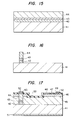
- Figure 13 shows the state in which the electrodes were disposed.
- a positive type photoresist film was formed to a thickness of 1.2 pm and was provided with openings for forming terminal portions for the external lead-out of the electrodes 36 and 37 and a short-circuit portion between the electrodes 35 and 38.
- the exposed Si0 2 film was etched down to a thickness of 150 nm.
- Cr and Au were respectively evaporated 60 nm and 300 nm as leads 39 and 39' and the external lead-out terminal portions. (The leads 39 and 39' are connected though the connection is not clearly shown on account of the way of taking the section.)
- an Au-Ge alloy was evaporated to form an n-side electrode 40.
- the crystal was cleaved along planes perpendicular to the traveling direction of laser radiation, to construct an optical resonator.
- the cavity length was made 300 ⁇ m.
- This light emitting device could be caused to perform laser oscillation by applying a voltage of 4 - 5 V across the drain electrode 36 and the n-side electrode 40 of the laser element.
- the oscillation wavelength was 830 nm, and the threshold current was approximately 60 mA.
- the two FETs in the semiconductor light emitting device had specifications as stated below.
- One FET (5) had a source - drain distance of 6 ⁇ m, and a gate length of 2 ⁇ m.
- the mutual conductance g m of the FET was great and 15 ms, and a current of 40 mA flowed during the zero bias of the gate.
- the FET (4) had a source - drain distance of 9 ⁇ m and a gate length of 3 /m.
- the mutual conductance g of this FET was 10 ms, and a current of 70 mA was obtained during the zero bias of the gate.
- TTL transistor-transistor logic
- this invention is not restricted to the GaAs-GaAlAs-based material but is realizable with other semiconductor materials.
- the semiconductor light emitting device of this invention can be realized with the following construction.
- an InP substrate used as a semiconductor substrate for growth is an InP substrate (doped with Sn, 3 x 10 18 /cm 3 ) whose upper surface is the (100) plane.
- an n-type InP layer T-doped, n ⁇ 3 x 10 18 /cm 3 ) being 3 fm thick as the first semiconductor layer
- a p-type In 0.73 Ga 0.27 As 0.59 P 0.41 layer(doped with Zn, p ⁇ 1 x 10 18 /cm 3 ) being 0.2 ⁇ m as the second semiconductor layer
- a p-type InP layer doped with Z n, p ⁇ 2 x 10 18 / cm 3
- an InP layer p ⁇ 10 14 /cm 3
- an n-type InP layer (doped with Sn, n ⁇ 1 ⁇ 1
- Zn is diffused in the electrode lead-out portion of the semiconductor laser portion.
- An Au-Zn electrode is used as the p-side electrode of the laser portion, an Au-Ge electrode as the n-side electrode thereof, a Schottky electrode of Cr-Au as the gate electrode, and Au-Ge electrodes as the source and drain electrodes.
- a semiconductor light emitting device having an oscillation wavelength of 1.3 ⁇ m and a threshold current of 100 mA could be realized and could be modulated at 2 GHz.
- Figures 15 to 17 are views of manufacturing steps showing another embodiment of this invention.
- a plan view of this example is similar to Figure 7.
- An SiO 2 film having a thickness of 500 nm was formed on the surface of the third semiconductor layer 44 by the CVD process.
- the SiO 2 film was etched to form a stripe having a width of 5 ⁇ m by the well-known photolithography.
- the semiconductor layers 42, 43 and 44 were etched with a liquid etchant which was a mixed solution consisting of phosphoric acid, hydrogen peroxide and water.
- Example 1 there were formed an SiO 2 film 53 as a passivation film, electrodes 47, 48, 49 and 50, a short-circuiting portion 52 between the electrodes 48 and 50, etc. Also materials may be those described before.
- n-side electrode 51 was formed on the rear surface of the semiconductor substrate 41.
- the crystal was cleaved along planes perpendicular to the traveling direction of laser radiation, to construct an optical resonator.
- the cavity length was made 300 ⁇ m.
- Figure 17 is a sectional view of the device at this time.
- the threshold current value of the fabricated laser was 10 - 30 mA, and the output power could be varied in a range of 3 mW - 0 mW by varying the gate voltage over a range of 0 to 0.6 V.
- a semi-insulating semiconductor substrate is used to form an FET portion therein, whereas a semiconductor laser element portion is formed on a semiconductor substrate.
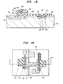
- Figure 18 is a sectional view of a device illustrative of such an example.
- the laser element portion and one FET portion have been appropriately taken as a section likewise to, for example, Figure 8.
- a semi-insulating GaAs substrate 81 was implanted with Si (Sn, Se or the like may well be employed) by the ion implantation, to form a shallow n-type impurity region 84. Subsequently, S was ion-implanted in correspondence with an electrode leading-out part 82 of the laser element and parts 83 and 85 of the FET portion, to form deep and heavily-doped n-type impurity regions (hereinbelow, termed "n + impurity regions”) 82, 83 and 85. These steps may conform with a method used in the field of conventional semiconductor devices. Subsequently, there were formed semiconductor layers constituting the semiconductor laser portion, i.
- an n-type Ga 0.7 Al 0.3 As layer 86 first semiconductor layer
- an n-type GaAs layer 87 second semiconductor layer
- a p-type Ga 0.7 Al 0.3 As layer 88 third semiconductor layer
- an n-type GaAs layer 89 fourth semiconductor layer.
- the stacked semiconductor layers were mesa-etched, to leave an area to construct the laser portion.
- a Zn-diffused region reaching the semiconductor layer 88 was formed.
- a Schottky electrode 92 for the FET was formed, and further, an SiO 2 film was formed as an insulating film 96 by the CVD process.
- Openings were provided in predetermined parts of the insulating film 96, and ohmic electrodes 91 and 93 for the FET were formed. Further, a p-side electrode 90 for the laser element was formed. A lead 95 for short-circuiting the p-side electrode 90 for the laser element and the source electrode 91 of the FET, an n-side lead-out electrode 94 for the laser element, and a drain lead-out electrode 97 and a gate lead-out electrode (not shown) of the FET were formed.
- Figure 19 is a plan view of this example. In Figure 19, the same numerals as in Figure 18 indicate the same parts. Dashed numerals 91', 92', 93' and 96' correspond to the parts 91, 92, 93 and 96 of the other FET, respectively.
- Figure 20 shows an example in which the FET portion was formed on a semiconductor substrate.
- the source electrode of the FET was grounded.
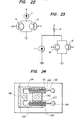
- Figure 22 shows an equivalent circuit of this composite device.
- Numeral 1 designates a.semiconductor laser
- numerals 4 and 5 designate FETs respectively
- numerals 6 and 7 designate the gate electrodes of the respective FETs.
- a shallow n-type impurity region 63 employing Si or the like and deep n impurity regions 62 and 64 employing S or the like.
- the n + impurity region 62 served both as the drain of the FET and as the interconnection for short-circuiting the drain of the FET and the n-side electrode of the semiconductor laser.
- numerals 65, 66, 67 and 68 indicate an n-type Ga 0.7 Al 0.3 As layer, an n-type GaAs layer, a p-type Ga 0.7 Al 0.3 As layer and an n-type GaAs layer, respectively.
- Numeral 71 indicates a Schottky electrode for the FET gate electrode, and numeral 72 a source electrode.
- Numeral 74 indicates an insulating film, and numerals 70 and 73 indicate external lead-out electrodes respectively.
- Figure 21 shows an example which employed a semi-insulating substrate.
- a semiconductor laser element portion and an FET portion were disposed on the substrate.
- an n-type GaAs layer 102 doped with Sn was formed and had a semiconductor laser element portion and an FET portion formed thereon.
- the other construction was the same as in the foregoing example. More specifically, numerals 103, 104, 105 and 106 designate first to fourth semiconductor layers constituting the semiconductor laser element respectively.
- Numerals 108, 109 and 110 designate the drain, gate and source electrodes of the FET respectively
- numeral 114 designates an insulating layer
- numerals 111, 112, and 113 designate an n-side electrode of the semiconductor laser, an interconnection for short-circuiting a p-side electrode 107 of the semiconductor laser and the drain electrode of the FET, and a source lead-out electrode of the FET, respectively.
- a semiconductor light emitting device of an equivalent circuit shown in Figure 23 can accomplish the same subject matter as in the examples thus far described.
- two FETs (16, 17) are integrated and disposed in parallel.
- a voltage is applied to the drain electrodes of the two FETs through a resistor 14.
- a D.C. bias is applied to the FET (16), and is adjusted so that the current value may become slightly smaller than the oscillation threshold value of the semiconductor laser (1).
- the FET (17) becomes a high resistance, so that the current on the semiconductor laser side increases to induce laser oscillation.
- Figure 24 is a plan view of this example.
- Numerals 121 and 125 designate drain electrodes, numerals 122 and 126 gate electrodes, numerals 123 and 127 source electrodes, and numerals 124 and 128 leads which connect with a p-side electrode 129 of the semiconductor laser element.
- the electrode 129 is connected to a power source through a resistor.
- Shown at 130 is a lead for short-circuiting and grounding the source electrodes of the FETS.
Landscapes
- Physics & Mathematics (AREA)
- Condensed Matter Physics & Semiconductors (AREA)
- General Physics & Mathematics (AREA)
- Electromagnetism (AREA)
- Optics & Photonics (AREA)
- Semiconductor Lasers (AREA)
Applications Claiming Priority (2)
| Application Number | Priority Date | Filing Date | Title |
|---|---|---|---|
| JP14657879A JPS5670681A (en) | 1979-11-14 | 1979-11-14 | Semiconductor luminous element |
| JP146578/79 | 1979-11-14 |
Publications (3)
| Publication Number | Publication Date |
|---|---|
| EP0029228A2 true EP0029228A2 (de) | 1981-05-27 |
| EP0029228A3 EP0029228A3 (en) | 1983-03-30 |
| EP0029228B1 EP0029228B1 (de) | 1987-09-16 |
Family
ID=15410858
Family Applications (1)
| Application Number | Title | Priority Date | Filing Date |
|---|---|---|---|
| EP80107031A Expired EP0029228B1 (de) | 1979-11-14 | 1980-11-13 | Laser-Halbleitervorrichtung |
Country Status (5)
| Country | Link |
|---|---|
| US (1) | US4366567A (de) |
| EP (1) | EP0029228B1 (de) |
| JP (1) | JPS5670681A (de) |
| CA (1) | CA1152197A (de) |
| DE (1) | DE3072032D1 (de) |
Cited By (2)
| Publication number | Priority date | Publication date | Assignee | Title |
|---|---|---|---|---|
| DE3242076A1 (de) * | 1982-11-13 | 1984-05-17 | ANT Nachrichtentechnik GmbH, 7150 Backnang | Optoelektronisches bauelement |
| EP0487192A3 (en) * | 1990-11-19 | 1992-12-02 | Mitsubishi Denki Kabushiki Kaisha | Opto-electronic integrated circuit having a transmitter of long wavelength |
Families Citing this family (20)
| Publication number | Priority date | Publication date | Assignee | Title |
|---|---|---|---|---|
| JPS5821887A (ja) * | 1981-08-03 | 1983-02-08 | Agency Of Ind Science & Technol | 半導体発光素子の製造方法 |
| JPS5856489A (ja) * | 1981-09-30 | 1983-04-04 | Fujitsu Ltd | 半導体発光装置 |
| JPS5892259A (ja) * | 1981-11-27 | 1983-06-01 | Fujitsu Ltd | 複合半導体装置 |
| JPS58170054A (ja) * | 1982-03-31 | 1983-10-06 | Fujitsu Ltd | 光複合半導体装置 |
| JPS596587A (ja) * | 1982-07-05 | 1984-01-13 | Agency Of Ind Science & Technol | 半導体レ−ザ装置 |
| JPS5943589A (ja) * | 1982-09-03 | 1984-03-10 | Agency Of Ind Science & Technol | プレ−ナ型光電子集積回路 |
| US4608696A (en) * | 1983-06-08 | 1986-08-26 | Trw Inc. | Integrated laser and field effect transistor |
| JPS6059791A (ja) * | 1983-09-13 | 1985-04-06 | Toyota Central Res & Dev Lab Inc | 集積化光半導体装置 |
| JPS61273015A (ja) * | 1985-05-29 | 1986-12-03 | Hitachi Ltd | 電流切替回路 |
| US4709370A (en) * | 1985-06-17 | 1987-11-24 | Rca Corporation | Semiconductor laser driver circuit |
| FR2592739B1 (fr) * | 1986-01-06 | 1988-03-18 | Brillouet Francois | Structure semi-conductrice monolithique d'un laser et d'un transistor a effet de champ et son procede de fabrication |
| EP0293185B1 (de) * | 1987-05-26 | 1994-02-02 | Kabushiki Kaisha Toshiba | Halbleiterlaservorrichtung und Verfahren zu ihrer Herstellung |
| US4996163A (en) * | 1988-02-29 | 1991-02-26 | Sumitomo Electric Industries, Ltd. | Method for producing an opto-electronic integrated circuit |
| US5003359A (en) * | 1989-12-29 | 1991-03-26 | David Sarnoff Research Center, Inc. | Optoelectronic integrated circuit |
| US4995049A (en) * | 1990-05-29 | 1991-02-19 | Eastman Kodak Company | Optoelectronic integrated circuit |
| US5305338A (en) * | 1990-09-25 | 1994-04-19 | Mitsubishi Denki Kabushiki Kaisha | Switch device for laser |
| JPH05346179A (ja) * | 1991-12-14 | 1993-12-27 | Sumitomo Rubber Ind Ltd | タイヤ用空気充填器具 |
| JPH0740130Y2 (ja) * | 1992-12-24 | 1995-09-13 | ハン ヤン ケミカル コーポレイション | エア注入用バルブ装置 |
| AU4695096A (en) * | 1995-01-06 | 1996-07-24 | National Aeronautics And Space Administration - Nasa | Minority carrier device |
| DE102004038405A1 (de) * | 2004-08-07 | 2006-03-16 | Fraunhofer-Gesellschaft zur Förderung der angewandten Forschung e.V. | Quantenkaskadenlaser mit reduzierter Verlustleistung |
Family Cites Families (1)
| Publication number | Priority date | Publication date | Assignee | Title |
|---|---|---|---|---|
| DE2330310A1 (de) * | 1973-06-14 | 1975-01-16 | Siemens Ag | Verfahren zur pulsmodulation von halbleiterlasern |
-
1979
- 1979-11-14 JP JP14657879A patent/JPS5670681A/ja active Granted
-
1980
- 1980-11-05 US US06/204,231 patent/US4366567A/en not_active Expired - Lifetime
- 1980-11-13 EP EP80107031A patent/EP0029228B1/de not_active Expired
- 1980-11-13 DE DE8080107031T patent/DE3072032D1/de not_active Expired
- 1980-11-14 CA CA000364710A patent/CA1152197A/en not_active Expired
Cited By (3)
| Publication number | Priority date | Publication date | Assignee | Title |
|---|---|---|---|---|
| DE3242076A1 (de) * | 1982-11-13 | 1984-05-17 | ANT Nachrichtentechnik GmbH, 7150 Backnang | Optoelektronisches bauelement |
| EP0487192A3 (en) * | 1990-11-19 | 1992-12-02 | Mitsubishi Denki Kabushiki Kaisha | Opto-electronic integrated circuit having a transmitter of long wavelength |
| US5311046A (en) * | 1990-11-19 | 1994-05-10 | Mitsubishi Denki Kabushiki Kaisha | Long wavelength transmitter opto-electronic integrated circuit |
Also Published As
| Publication number | Publication date |
|---|---|
| CA1152197A (en) | 1983-08-16 |
| JPS6359277B2 (de) | 1988-11-18 |
| EP0029228B1 (de) | 1987-09-16 |
| EP0029228A3 (en) | 1983-03-30 |
| JPS5670681A (en) | 1981-06-12 |
| US4366567A (en) | 1982-12-28 |
| DE3072032D1 (en) | 1987-10-22 |
Similar Documents
| Publication | Publication Date | Title |
|---|---|---|
| EP0029228B1 (de) | Laser-Halbleitervorrichtung | |
| CA1138561A (en) | Semiconductor light emitting element and method for producing the same | |
| US5202896A (en) | Bipolar inversion channel field effect transistor laser | |
| US6936486B2 (en) | Low voltage multi-junction vertical cavity surface emitting laser | |
| US4430741A (en) | Semiconductor laser device | |
| US4752934A (en) | Multi quantum well laser with parallel injection | |
| EP0000412B1 (de) | Halbleiter-Injektionslaser oder-verstärker | |
| US4278949A (en) | Semiconductor laser structure and manufacture | |
| JPH0553317B2 (de) | ||
| US4958202A (en) | Semiconductor light-emitting device and method of manufacturing the same | |
| GB2252872A (en) | Laser diode and method of manufacture | |
| US4677634A (en) | Double heterojunction semiconductor laser having improved high-frequency characteristics | |
| US4829534A (en) | Semiconductor laser device having a semiconductor region for creating a depletion layer in a laser active layer for controlling current flow therethrough | |
| EP0487192A2 (de) | Optoelektronische integrierte Schaltung mit einem Langwellensender | |
| US5149670A (en) | Method for producing semiconductor light emitting device | |
| US4941024A (en) | Semiconductor apparatus | |
| US4858241A (en) | Semiconductor laser device | |
| JPS6237906B2 (de) | ||
| Matsueda et al. | Integration of a laser diode and a twin FET | |
| JPH023314B2 (de) | ||
| Bouley | Lasers for integrated optoelectronics | |
| JP2517042B2 (ja) | 光集積回路 | |
| JPS63301583A (ja) | 半導体発光素子 | |
| JPH01103893A (ja) | 半導体レーザ装置 | |
| Lee | New optoelectronic devices using GaAs-GaAlAs epitaxy |
Legal Events
| Date | Code | Title | Description |
|---|---|---|---|
| PUAI | Public reference made under article 153(3) epc to a published international application that has entered the european phase |
Free format text: ORIGINAL CODE: 0009012 |
|
| AK | Designated contracting states |
Designated state(s): DE FR GB NL |
|
| 17P | Request for examination filed |
Effective date: 19811015 |
|
| PUAL | Search report despatched |
Free format text: ORIGINAL CODE: 0009013 |
|
| AK | Designated contracting states |
Designated state(s): DE FR GB NL |
|
| GRAA | (expected) grant |
Free format text: ORIGINAL CODE: 0009210 |
|
| AK | Designated contracting states |
Kind code of ref document: B1 Designated state(s): DE FR GB NL |
|
| PG25 | Lapsed in a contracting state [announced via postgrant information from national office to epo] |
Ref country code: NL Effective date: 19870916 |
|
| REF | Corresponds to: |
Ref document number: 3072032 Country of ref document: DE Date of ref document: 19871022 |
|
| ET | Fr: translation filed | ||
| NLV1 | Nl: lapsed or annulled due to failure to fulfill the requirements of art. 29p and 29m of the patents act | ||
| PLBE | No opposition filed within time limit |
Free format text: ORIGINAL CODE: 0009261 |
|
| STAA | Information on the status of an ep patent application or granted ep patent |
Free format text: STATUS: NO OPPOSITION FILED WITHIN TIME LIMIT |
|
| 26N | No opposition filed | ||
| PGFP | Annual fee paid to national office [announced via postgrant information from national office to epo] |
Ref country code: GB Payment date: 19980930 Year of fee payment: 19 |
|
| PGFP | Annual fee paid to national office [announced via postgrant information from national office to epo] |
Ref country code: FR Payment date: 19981117 Year of fee payment: 19 |
|
| PGFP | Annual fee paid to national office [announced via postgrant information from national office to epo] |
Ref country code: DE Payment date: 19990125 Year of fee payment: 19 |
|
| PG25 | Lapsed in a contracting state [announced via postgrant information from national office to epo] |
Ref country code: GB Free format text: LAPSE BECAUSE OF NON-PAYMENT OF DUE FEES Effective date: 19991113 |
|
| GBPC | Gb: european patent ceased through non-payment of renewal fee |
Effective date: 19991113 |
|
| PG25 | Lapsed in a contracting state [announced via postgrant information from national office to epo] |
Ref country code: FR Free format text: LAPSE BECAUSE OF NON-PAYMENT OF DUE FEES Effective date: 20000731 |
|
| PG25 | Lapsed in a contracting state [announced via postgrant information from national office to epo] |
Ref country code: DE Free format text: LAPSE BECAUSE OF NON-PAYMENT OF DUE FEES Effective date: 20000901 |
|
| REG | Reference to a national code |
Ref country code: FR Ref legal event code: ST |