EP0050064A2 - Transistor à effet de champ à fréquence de coupure élevée - Google Patents
Transistor à effet de champ à fréquence de coupure élevée Download PDFInfo
- Publication number
- EP0050064A2 EP0050064A2 EP81401484A EP81401484A EP0050064A2 EP 0050064 A2 EP0050064 A2 EP 0050064A2 EP 81401484 A EP81401484 A EP 81401484A EP 81401484 A EP81401484 A EP 81401484A EP 0050064 A2 EP0050064 A2 EP 0050064A2
- Authority
- EP
- European Patent Office
- Prior art keywords
- layer
- semiconductor
- field effect
- effect transistor
- doped
- Prior art date
- Legal status (The legal status is an assumption and is not a legal conclusion. Google has not performed a legal analysis and makes no representation as to the accuracy of the status listed.)
- Granted
Links
Images


Classifications
-
- H—ELECTRICITY
- H10—SEMICONDUCTOR DEVICES; ELECTRIC SOLID-STATE DEVICES NOT OTHERWISE PROVIDED FOR
- H10D—INORGANIC ELECTRIC SEMICONDUCTOR DEVICES
- H10D62/00—Semiconductor bodies, or regions thereof, of devices having potential barriers
- H10D62/80—Semiconductor bodies, or regions thereof, of devices having potential barriers characterised by the materials
- H10D62/82—Heterojunctions
- H10D62/824—Heterojunctions comprising only Group III-V materials heterojunctions, e.g. GaN/AlGaN heterojunctions
-
- H—ELECTRICITY
- H10—SEMICONDUCTOR DEVICES; ELECTRIC SOLID-STATE DEVICES NOT OTHERWISE PROVIDED FOR
- H10D—INORGANIC ELECTRIC SEMICONDUCTOR DEVICES
- H10D30/00—Field-effect transistors [FET]
- H10D30/40—FETs having zero-dimensional [0D], one-dimensional [1D] or two-dimensional [2D] charge carrier gas channels
- H10D30/47—FETs having zero-dimensional [0D], one-dimensional [1D] or two-dimensional [2D] charge carrier gas channels having two-dimensional [2D] charge carrier gas channels, e.g. nanoribbon FETs or high electron mobility transistors [HEMT]
- H10D30/471—High electron mobility transistors [HEMT] or high hole mobility transistors [HHMT]
- H10D30/473—High electron mobility transistors [HEMT] or high hole mobility transistors [HHMT] having confinement of carriers by multiple heterojunctions, e.g. quantum well HEMT
- H10D30/4732—High electron mobility transistors [HEMT] or high hole mobility transistors [HHMT] having confinement of carriers by multiple heterojunctions, e.g. quantum well HEMT using Group III-V semiconductor material
- H10D30/4738—High electron mobility transistors [HEMT] or high hole mobility transistors [HHMT] having confinement of carriers by multiple heterojunctions, e.g. quantum well HEMT using Group III-V semiconductor material having multiple donor layers
-
- H—ELECTRICITY
- H10—SEMICONDUCTOR DEVICES; ELECTRIC SOLID-STATE DEVICES NOT OTHERWISE PROVIDED FOR
- H10D—INORGANIC ELECTRIC SEMICONDUCTOR DEVICES
- H10D30/00—Field-effect transistors [FET]
- H10D30/40—FETs having zero-dimensional [0D], one-dimensional [1D] or two-dimensional [2D] charge carrier gas channels
- H10D30/47—FETs having zero-dimensional [0D], one-dimensional [1D] or two-dimensional [2D] charge carrier gas channels having two-dimensional [2D] charge carrier gas channels, e.g. nanoribbon FETs or high electron mobility transistors [HEMT]
- H10D30/471—High electron mobility transistors [HEMT] or high hole mobility transistors [HHMT]
- H10D30/475—High electron mobility transistors [HEMT] or high hole mobility transistors [HHMT] having wider bandgap layer formed on top of lower bandgap active layer, e.g. undoped barrier HEMTs such as i-AlGaN/GaN HEMTs
- H10D30/4755—High electron mobility transistors [HEMT] or high hole mobility transistors [HHMT] having wider bandgap layer formed on top of lower bandgap active layer, e.g. undoped barrier HEMTs such as i-AlGaN/GaN HEMTs having wide bandgap charge-carrier supplying layers, e.g. modulation doped HEMTs such as n-AlGaAs/GaAs HEMTs
-
- H—ELECTRICITY
- H10—SEMICONDUCTOR DEVICES; ELECTRIC SOLID-STATE DEVICES NOT OTHERWISE PROVIDED FOR
- H10D—INORGANIC ELECTRIC SEMICONDUCTOR DEVICES
- H10D62/00—Semiconductor bodies, or regions thereof, of devices having potential barriers
- H10D62/10—Shapes, relative sizes or dispositions of the regions of the semiconductor bodies; Shapes of the semiconductor bodies
- H10D62/13—Semiconductor regions connected to electrodes carrying current to be rectified, amplified or switched, e.g. source or drain regions
- H10D62/149—Source or drain regions of field-effect devices
Definitions
- the present invention relates to field effect transistors, and more particularly those with a high cut-off frequency.
- transistors of the family of III-V semiconductors, transistors have been described comprising, supported by a semi-insulating substrate, on the one hand the access regions, called source and drain, and d on the other hand, a control region constituted by an active layer of lightly doped GaAs and in juxtaposition with a layer of Al x Ga 1-x As.
- These transistors all have the particularity of exhibiting a strong accumulation of electrons in the layer of GaAs due to the existence of heterojunction and a high mobility of electrons in the transistor channel, between source and drain, due to the low doping of the active layer in GaAs. Thus these transistors have a high cut-off frequency.
- French patent applications Nos In French patent applications Nos.
- an insulating layer is interposed between the gate contact metal and the Al x Ga 1-x As layer.
- the Schottky gate contact is deposited on a layer of GaAs, the layer of Al x Ga 1-x As being located between the semi-insulating substrate and the active layer of GaAs.
- transistors relate only to active GaAs layers.
- materials having a higher mobility than GaAs they are for example In As, In Sb or their alloys of the type Ga x In 1-x As or In As Sb 1-x .
- these materials if they are weakly doped, have 20,000, 80,000, 15,000 and 50,000 cm vs respectively. The last two values correspond to compositions such as x ⁇ 0.5.
- lightly doped GaAs has a mobility of 8000 cm 2 v -1 s -1 . It is therefore interesting to use these materials as an active part of the channel of a field effect transistor.
- Ga In 1-x As field effect transistors have already been described in the literature. These are MESFET (Metal Schottky field effect transistor) or junction (JFET) transistors in which the active layer is doped at approximately 10 17 atoms / cm 3 and in which the electronic mobility is close to 10,000 cm 2 vs - 1 . To achieve a mobility of 15,000 cm 2 v -1 s-1, Ga x In 1-x As must be lightly doped according to heterojunction structures described in patent applications No. 79.07 803, 79.22 586, 79.22 301 and 79.22. 611, of the plaintiff.
- the object of the present invention is to remedy these limitations by a particular structure of the field effect transistor channel, this channel comprising, in addition to the Schottky gate, a heterojunction. formed between a first semiconductor material such as Ga In, 1-x As and a second semiconductor material, of the family of compounds III-V having the same crystal lattice parameter as Ga x In 1-x As but with a larger band gap, the pair of materials thus forming an N - N heterojunction and having an electron accumulation layer in Ga x In 1-x As.
- a first semiconductor material such as Ga In, 1-x As
- a second semiconductor material of the family of compounds III-V having the same crystal lattice parameter as Ga x In 1-x As but with a larger band gap
- the invention consists of a field effect transistor with a high cut-off frequency, comprising, supported by a semi-insulating substrate, two access regions called source and drain and a control region composed of a first active layer, a second layer and a so-called Schottky metal grid, the second layer being located between the first layer and the metal grid, this transistor being characterized in that the first layer, of a material semiconductor of a first family, and the second layer, of a semiconductor material of a second family form an isotype NN heterojunction, in which the second family semiconductor material has the same crystal lattice parameter and a larger band gap than the semiconductor material of the first family, and in that the first layer is doped at a level lower, or equal, to 10 16 atoms / cm 3 and the second layer is doped at a level higher, or equal, to 10 atoms / cm.
- FIG. 1 represents a heterostructure composed, on the one hand, of an isotype heterojunction formed of a first semiconductor 1 of type N and of a second semiconductor 2 of type N also, having a larger forbidden band than the first semiconductor 1 but having the same lattice parameter as the latter and, on the other hand, of a Schottky contact formed between a metal and the second semiconductor 2.
- the system is at equilibrium, say that the Fermi E F levels are aligned.
- E and E respectively represent the energy levels of the conduction band and of valence, and ⁇ E c represents the discontinuity in the conduction band.
- ⁇ E c represents the discontinuity in the conduction band.
- the system is subjected to a negative voltage V on the metal.
- V a voltage sufficiently large in absolute value
- the region 5 of space charge extends to the interface of the heterojunction, thus destroying the accumulation layer 3 to reveal a zone 6 deserted by electrons .
- the semiconductor 1 is Ga x In 1-x As
- its composition must be such that its lattice parameter is adapted to a known substrate so as to obtain an epitaxial layer of good qualities.
- the substrates in GaAs or InAs being obviously excepted since their lattice parameter is different from that of Ga x In 1-x As.
- the alloy Ga x In 1-x As is adapted in lattice parameter with InP.
- the Ga x In 1-x As alloy has a band gap of about 0.75 eV for x ⁇ 0.5.
- the semiconductor 2 with a forbidden band larger than Ga x In 1-x As can therefore be InP, (forbidden band 1 , 36 eV ) Al x In 1-x As ( x 0 , 5 ) (forbidden band 1.46 eV) , GaAs Sb (y ⁇ 0.5), AlAs y Sb 1-y (y ⁇ 0.5) or quaternary alloys Ga x In 1-x As y P 1-y , Al x Ga 1-x As y Sb 1-y .
- These semiconductors with a large forbidden band, semiconductors 2 should be called.
- FIG. 3 represents in schematic section, the first example of a transistor according to the invention.
- the layer 8 is lightly doped at a level below 10 16 atoms / cm 3 and the layer 9 is doped at a level higher than 10 17 a t ome s / cm 3 .
- the source and drain electrodes 10 are deposited on either side of the Schottky grid electrode 12. As explained in Figures 1 and 2, electrons accumulate in layer 8 of GaInAs and desert layer 9.
- the thickness of layer 8 is equal to the thickness of the accumulation zone (approximately 0.1 ⁇ m) and that of layer 9 equal to the thickness of the deserted area (approximately 0.1 ⁇ m).
- the modulation of the source-drain current is done through the gate bias.
- the transistor described operates at high frequency according to the basis of the invention.
- the interface between a semi-insulating substrate and an active layer contains electrically active faults. It is therefore advantageous to intercalate between the substrate 7 and the layer 8 of GaInAs an epitaxial layer of high resistivity called the buffer layer, so as to eliminate these local defects.
- FIG. 4 represents a second example of a transistor, provided with a first improvement, according to the invention.
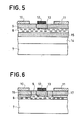
- FIG. 5 represents a third example of a transistor provided with a second improvement according to the invention.
- This transistor comprises, in addition to the elements described in the second example, a semiconductor layer 15 interposed between the active layer 8 and the buffer layer 14.
- the layer 15 is doped with type N at a level greater than 10 17 atoms / cm 3 in order to increase the density of electrons accumulated in layer 8 of GaInAs. This increases the transconductance of the device.
- the thickness of layer 15 is equal to the thickness of the deserted area of electrons in the heterojunction (approximately 0.1 ⁇ m).
- the ohmic contacts 10 of source and 11 of drain are deposited on the semiconductor 2. Now there is a potential barrier at E that the electrons must cross to go from the source to the drain. In general ⁇ E C is low enough for the electrons to cross it, however this barrier decreases the source-drain conductance.
- the apparent height of the heterojunction barrier is reduced by the tunnel effect by strongly doping the semiconductor 2, in the regions located under the source and the drain.
- FIG. 6 represents such a structure in which the wells 16 and 17 located under the contacts, heavily doped (greater than 10 18 atoms / cm 3 ), are obtained by implantations before depositing the contacts 10 and 11. To be fully effective, it the wells 16 and 17 must enter the active layer 8. The wells 16 and 17 also make it possible to reduce the source and drain contact resistances and the series resistances formed by the thickness of the layer 9 under the source and the drain.
- the substrate consists of InP.
- the transistors according to the invention find their applications in all microwave fields, in particular telecommunications.
Landscapes
- Junction Field-Effect Transistors (AREA)
- Bipolar Transistors (AREA)
Abstract
Description
- La présente invention concerne les transistors à effet de champ, et plus particulièrement ceux dont la fréquence de coupure est élevée.
- Parmi les transistors à effet de champ connus, de la famille des semiconducteurs III-V, ont été décrits des transistors comportant, supportées par un substrat semi-isolant, d'une part les régions d'accès, dites source et drain, et d'autre part, une région de commande constituée par une couche active en GaAs faiblement dopée et en juxtaposition avec une couche en Alx Ga1-xAs. Ces transistors possèdent tous la particularité de présenter une forte accumulation d'électrons dans la couche de GaAs du fait de l'existence de l'hétérojonction et une forte mobilité d'électrons dans le canal du transistor, entre source et drain, du fait du faible dopage de la couche active en GaAs. Ainsi ces transistors ont une fréquence de coupure élevée. Dans les demandes de brevet français n° 79.22 301 et 79.26 611, de la demanderesse, une couche d'isolant est intercalée entre le métal de contact de grille et la couche en AlxGa1-xAs. Dans la demande de brevet français N° 79.22 586, de la demanderesse, le contact de grille Schottky est déposé sur une couche en GaAs, la couche en AlxGa1-xAs étant située entre le substrat semi-isolant et la couche active en GaAs.
- Ces transistors ne concernent que des couches actives en GaAs. Il existe dans la famille des composés semiconducteurs III-V, des matériaux ayant une plus forte mobilité que GaAs : ce sont par exemple In As, In Sb ou leurs alliages du type GaxIn1-xAs ou In As Sb1-x. A la température ambiante ces matériaux, s'ils sont faiblement dopés, ont respectivement pour mobilité 20 000 , 80 000, 15 000 et 50 000 cm v s . Les deux dernières valeurs correspondent à des compositions telles que x ≃0,5. A titre de comparaison, GaAs faiblement dopé a une mobilité de 8 000 cm2 v-1 s-1. Il est alors intéressant d'utiliser ces matériaux comme partie active du canal d'un transistor à effet de champ.
- Des transistors à effet de champ en Ga In1-xAs ont été déjà décrits dans la littérature. Il s'agit des transistors MESFET (Metal Schottky field effect transistor) ou à jonction (JFET) dans lesquels la couche active est dopée à 1017 atomes/cm3 environ et dans lesquels la mobilité électronique est voisine de 10 000 cm2 v s-1. Pour atteindre une mobilité de 15 000 cm2 v-1 s-1 il faut utiliser GaxIn1-xAs faiblement dopé selon des structures à hétérojonction décrites dans les demandes de brevet n° 79.07 803, 79.22 586, 79.22 301 et 79.22 611, de la demanderesse.
- Cependant ces semiconducteurs connus ont des bandes interdites de faible largeur, ce qui entraine les difficultés suivantes :
- - pour ceux qui utilisent InAs, InSb et les alliages InAs1-xSbx, les bandes interdites sont si faibles (de 0,23 à 0,41 eV) qu'il est exclus de travailler à la température ambiante. A basse température (77°K) l'avantage de la forte mobilité par rapport à GaAs n'est plus valable. De ce point de vue, InAs, InSb et InAs1-xSbx ne présentent pas d'intérêt, mais GaxIn1-xAs reste intéressant.
- - les grilles Schottky déposées sur ces matériaux présentent des courants de fuite élevés. Ce qui exclut son utilisation selon l'une des structures décrites dans la demande de brevet n° 79.22 586.
- L'objet de la présente invention est de remédier à ces limitations par une structure particulière de canal de transistor à effet de champ, ce canal comprenant, outre la grille Schottky, une hétérojonction. formée entre un premier matériau semiconducteur tel que Ga In, 1-xAs et un second matériau semiconducteur, de la famille des composés III-V ayant même paramètre de maille cristalline que GaxIn1-xAs mais de bande interdite plus grande, le couple de matériaux formant ainsi une hétérojonction N - N et présentant une couche d'accumulation d'électrons dans GaxIn1-xAs.
- De façon plus précise, l'invention consiste en un transistor à effet de champ à fréquence de coupure élevée, comportant, supportées par un substrat semi-isolant, deux régions d'accès dites de source et de drain et une région de commande composée d'une première couche active, d'une seconde couche et d'une grille métallique dite de Schottky, la seconde couche étant située entre la première couche et la grille métallique, ce transistor étant caractérisé en ce que la première couche, d'un matériau semiconducteur d'une première famille, et la seconde couche, d'un matériau semiconducteur d'une seconde famille forment une hétérojonction isotype N-N, dans laquelle le matériau semiconducteur de seconde famille possède le même paramètre de maille cristalline et une bande interdite plus grande que le matériau semiconducteur de première famille, et en ce que la première couche est dopée à un niveau inférieur, ou égal, à 1016 atomes/cm3 et la seconde couche est dopée à un niveau supérieur, ou égal, à 10 atomes/cm .
- L'invention sera mieux comprise par la description qui suit, laquelle s'appuie sur des exemples de réalisation et sur les figures parmi lesquelles :
- - la figure 1 représente le schéma de bandes à l'équilibre, d'une hétérojonction comportant un semiconducteur à petite bande interdite, un semiconducteur à grande bande interdite et un métal ;
- - la figure 2 représente le schéma de bandes de l'hétérostructure sous polarisation négative du côté métal ;
- - la figure 3 représente en coupe schématique, un premier exemple de transistor selon l'invention ;
- - la figure 4 représente en coupe schématique, un deuxième exemple de transistor selon l'invention ;
- - la figure 5 représente en coupe schématique, un troisième exemple de transistor selon l'invention ;
- - la figure 6 représente en coupe schématique, un quatrième exemple de transistor selon l'invention.
- La figure 1 représente une hétérostructure composée, d'une part, d'une hétérojonction isotype formée d'un premier semiconducteur 1 de type N et d'un second semiconducteur 2 de type N également, ayant une bande interdite plus grande que le premier semiconducteur 1 mais présentant le même paramètre de maille que ce dernier et, d'autre part, d'un contact Schottky formé entre un métal et le second semiconducteur 2. Sur la figure 1, le système est à l'équilibre, c'est à dire que les niveaux de Fermi EF sont alignés.
- E et E représentent respectivement les niveaux d'énergie de la bande de conduction et de valence, et ΔEc représente la discontinuité dans la bande de conduction. Comme il a été déjà décrit dans les demandes de brevets n° 79.07 803, 79.22 586, 79.22 301 de la demanderesse, il existe à l'interface de l'hétérojonction une zone d'accumulation d'électrons du côté du semiconducteur 1 à petite bande interdite, et une couche de désertion d'électrons 4 du côté du semiconducteur 2 à grande bande interdite. Le semiconducteur 1 étant faiblement dopé, la mobilité des électrons dans la zone 3 est élevée. A l'interface métal-semiconducteur 2 il existe une zone 5 de désertion d'électrons.
- Sur la figure 2, le système est soumis à une tension V négative sur le métal. Pour une tension V suffisamment grande en valeur absolue, la région 5 de charge d'espace s'étend jusqu'à l'interface de l'hétérojonction, détruisant ainsi la couche d'accumulation 3 pour laisser apparaitre une zone 6 désertée d'électrons.
- Dans le cas précis où le semiconducteur 1 est GaxIn1-xAs, sa composition se doit être telle que son paramètre de maille soit adapté à un substrat connu de façon à obtenir une couche épitaxiale de bonnes qualités. Les substrats en GaAs ou InAs étant évidemment exceptés puisque leur paramètre de maille est différent de celui de GaxIn1-xAs. Pour x ≃ 0,5 l'alliage Ga xIn1-xAs est adapté en paramètre de maille avec InP. L'alliage Ga xIn1-x As a pour bande interdite environ 0,75 eV pour x ≃ 0,5. Le semiconducteur 2 à bande interdite plus grande que GaxIn1-xAs peut être donc InP, (bande interdite 1,36 eV) AlxIn1-xAs (x 0,5) (bande interdite 1,46 eV), GaAs Sb (y ≃ 0,5), AlAsySb1-y (y ≃ 0,5) ou des alliages quaternaires GaxIn1-xAsy P1-y, AlxGa1-xAsySb1-y. On conviendra d'appeler ces semiconducteurs à grande bande interdite, semiconducteurs 2.
- On conviendra également, dans le seul souci de simplification dû texte qui suit, d'écrire GaInAs au lieu de GaxIn1-xAs.
- La figure 3 représente en coupe schématique, le premier exemple de transistor selon l'invention.
- Sur un substrat 7, en InP par exemple, semi-isolant, sont déposées par épitaxie successivement une couche 8 en GaInAs et une couche 9 constituée d'un semiconducteur 2. La couche 8 est faiblement dopée à un niveau inférieur à 1016 atomes/cm3 et la couche 9 est dopée à un niveau supérieur à 1017 atomes/cm3. Les électrodes 10 de source et 11 de drain sont déposées de part et d'autre de l'électrode 12 de grille Schottky. Comme il a été expliqué à l'occasion des figures 1 et 2, des électrons s'accumulent dans la couche 8 de GaInAs et désertent la couche 9. Afin que seuls les électrons de la zone d'accumulation interviennent dans le fonctionnement du transistor, l'épaisseur de la couche 8 est égale à l'épaisseur de la zone d'accumulation (environ 0,1 µm) et celle de la couche 9 égale à l'épaisseur de la zone désertée (environ 0,1 µm). La modulation du courant source-drain se fait par l'intermédiaire de la polarisation de grille.
- Le transistor décrit fonctionne à haute fréquence selon le fondement de l'invention.
- Cependant, il est connu que l'interface entre un substrat semi-isolant et une couche active contient des défauts électriquement actifs. Il est donc avantageux d'intercaller entre le substrat 7 et la couche 8 de GaInAs une couche épitaxiale de haute résistivité appelée couche tampon, de façon à supprimer ces défauts locaux.
- La figure 4 représente un deuxième exemple de transistor, doté d'un premier perfectionnement, selon l'invention.
- Sa structure possède en plus de ce qui a été décrit dans l'exemple précédent, une couche tampon 14 en InP de haute résistivité ou en semiconducteur 2 de haute résistivité, intercalée entre le substrat 7 en InP semi-isolant et la couche active 8.
- La figure 5 représente un troisième exemple de transistor doté d'un second perfectionnement selon l'invention.
- Ce transistor comporte en plus des éléments décrits dans le second exemple, une couche 15 en semiconducteur 2 intercallé entre la couche active 8 et la couche tampon 14. La couche 15 est dopée de type N à un niveau supérieur à 1017 atomes/cm3 afin d'accroître la densité d'électrons accumulés dans la couche 8 en GaInAs. On augmente ainsi la transcon- ductance du dispositif. L'épaisseur de la couche 15 est égale à l'épaisseur de la zone désertée d'électrons dans l'hétérojonction (environ 0,1 µm).
- Dans les structures décrites précédemment, les contacts ohmiques 10 de source et 11 de drain sont déposés sur le semiconducteur 2. Or il existe une barrière de potentiel à E que les électrons doivent franchir pour aller de la source au drain. En général ΔEC est suffisamment faible pour que les électrons puissent la franchir, cependant cette barrière diminue la conductance source-drain.
- Afin d'accroître cette conductance, la hauteur apparente de barrière d'hétérojonction est réduite par effet tunnel en dopant fortement le semiconducteur 2, dans les régions situées sous la source et le drain.
- La figure 6 représente une telle structure dans laquelle les caissons 16 et 17 situés sous les contacts, fortement dopés (supérieurs à 1018 atomes/cm3), sont obtenus par implantations avant dépôt des contacts 10 et 11. Pour être pleinement efficaces, il faut que les caissons 16 et 17 pénètrent dans la couche active 8. Les caissons 16 et 17 permettent en plus de réduire les résistances de contact de source et de drain et les résistances séries constituées par l'épaisseur de la couche 9 sous la source et le drain.
- Les structures représentées dans les trois premiers exemples sont améliorées par l'adjonction des caissons 16 et 17, sous les contacts des régions d'accès.
- Dans les exemples de réalisation décrits, le substrat est constitué par InP. Cependant, appartiennent au domaine de l'invention les autres substrats, et les autres couches semiconductrices cités dans le texte à l'occasion de la figure 2, alliages ternaires et quaternaires, et qui sont précisés dans les revendications ci-après.
- Les transistors selon l'invention trouvent leurs applications dans tous les domaines hyperfréquences, notamment les télécommunications.
Claims (6)
Applications Claiming Priority (2)
| Application Number | Priority Date | Filing Date | Title |
|---|---|---|---|
| FR8021942A FR2492167A1 (fr) | 1980-10-14 | 1980-10-14 | Transistor a effet de champ a frequence de coupure elevee |
| FR8021942 | 1980-10-14 |
Publications (3)
| Publication Number | Publication Date |
|---|---|
| EP0050064A2 true EP0050064A2 (fr) | 1982-04-21 |
| EP0050064A3 EP0050064A3 (en) | 1982-05-05 |
| EP0050064B1 EP0050064B1 (fr) | 1985-05-02 |
Family
ID=9246865
Family Applications (1)
| Application Number | Title | Priority Date | Filing Date |
|---|---|---|---|
| EP81401484A Expired EP0050064B1 (fr) | 1980-10-14 | 1981-09-24 | Transistor à effet de champ à fréquence de coupure élevée |
Country Status (5)
| Country | Link |
|---|---|
| EP (1) | EP0050064B1 (fr) |
| JP (1) | JPS5795672A (fr) |
| CA (1) | CA1182930A (fr) |
| DE (1) | DE3170300D1 (fr) |
| FR (1) | FR2492167A1 (fr) |
Cited By (9)
| Publication number | Priority date | Publication date | Assignee | Title |
|---|---|---|---|---|
| FR2537781A1 (fr) * | 1982-12-14 | 1984-06-15 | Thomson Csf | Transistor a effet de champ, fonctionnant en regime d'accumulation par gaz d'electrons |
| EP0136108A1 (fr) * | 1983-08-31 | 1985-04-03 | Masataka Inoue | Dispositif semi-conducteur à hétérojonction |
| EP0171531A1 (fr) * | 1984-06-18 | 1986-02-19 | Hitachi, Ltd. | Dispositif semi-conducteur utilisant des électrons à haute mobilité |
| FR2572588A1 (fr) * | 1984-10-26 | 1986-05-02 | Int Standard Electric Corp | Photodetecteur integrable de facon monolithique |
| EP0257300A1 (fr) | 1986-07-21 | 1988-03-02 | Sumitomo Electric Industries Limited | Transistor à effet de champ |
| EP0264932A1 (fr) * | 1986-10-24 | 1988-04-27 | Sumitomo Electric Industries Limited | Transistor à effet de champ |
| WO1989005040A1 (fr) * | 1987-11-20 | 1989-06-01 | Bell Communications Research, Inc. | Triode semi-conductrice commandee par un champ de puits quantiques |
| US4837178A (en) * | 1984-10-31 | 1989-06-06 | Fujitsu Limited | Method for producing a semiconductor integrated circuit having an improved isolation structure |
| EP0397148A3 (fr) * | 1989-05-10 | 1991-05-15 | Fujitsu Limited | Dispositif à hétérostructure et procédé pour sa fabrication |
Families Citing this family (5)
| Publication number | Priority date | Publication date | Assignee | Title |
|---|---|---|---|---|
| JPS5913376A (ja) * | 1982-07-13 | 1984-01-24 | Nippon Telegr & Teleph Corp <Ntt> | ヘテロ接合を有する半導体薄膜 |
| JPS60113475A (ja) * | 1983-11-24 | 1985-06-19 | Fujitsu Ltd | 半導体装置 |
| JPH0714056B2 (ja) * | 1985-04-05 | 1995-02-15 | 日本電気株式会社 | 半導体装置 |
| JPH0216102Y2 (fr) * | 1985-05-17 | 1990-05-01 | ||
| JPS62145779A (ja) * | 1985-12-19 | 1987-06-29 | Sumitomo Electric Ind Ltd | 電界効果トランジスタ |
Family Cites Families (5)
| Publication number | Priority date | Publication date | Assignee | Title |
|---|---|---|---|---|
| US4160261A (en) * | 1978-01-13 | 1979-07-03 | Bell Telephone Laboratories, Incorporated | Mis heterojunction structures |
| US4163237A (en) * | 1978-04-24 | 1979-07-31 | Bell Telephone Laboratories, Incorporated | High mobility multilayered heterojunction devices employing modulated doping |
| FR2465318A1 (fr) * | 1979-09-10 | 1981-03-20 | Thomson Csf | Transistor a effet de champ a frequence de coupure elevee |
| CA1145482A (fr) * | 1979-12-28 | 1983-04-26 | Takashi Mimura | Dispositif a semiconducteur a heterojonction unique a grande mobilite electronique |
| JPS577165A (en) * | 1980-06-17 | 1982-01-14 | Fujitsu Ltd | Semiconductor device |
-
1980
- 1980-10-14 FR FR8021942A patent/FR2492167A1/fr active Granted
-
1981
- 1981-09-24 EP EP81401484A patent/EP0050064B1/fr not_active Expired
- 1981-09-24 DE DE8181401484T patent/DE3170300D1/de not_active Expired
- 1981-10-13 JP JP56163353A patent/JPS5795672A/ja active Pending
- 1981-10-13 CA CA000387748A patent/CA1182930A/fr not_active Expired
Cited By (10)
| Publication number | Priority date | Publication date | Assignee | Title |
|---|---|---|---|---|
| FR2537781A1 (fr) * | 1982-12-14 | 1984-06-15 | Thomson Csf | Transistor a effet de champ, fonctionnant en regime d'accumulation par gaz d'electrons |
| EP0136108A1 (fr) * | 1983-08-31 | 1985-04-03 | Masataka Inoue | Dispositif semi-conducteur à hétérojonction |
| EP0171531A1 (fr) * | 1984-06-18 | 1986-02-19 | Hitachi, Ltd. | Dispositif semi-conducteur utilisant des électrons à haute mobilité |
| FR2572588A1 (fr) * | 1984-10-26 | 1986-05-02 | Int Standard Electric Corp | Photodetecteur integrable de facon monolithique |
| US4837178A (en) * | 1984-10-31 | 1989-06-06 | Fujitsu Limited | Method for producing a semiconductor integrated circuit having an improved isolation structure |
| EP0257300A1 (fr) | 1986-07-21 | 1988-03-02 | Sumitomo Electric Industries Limited | Transistor à effet de champ |
| EP0264932A1 (fr) * | 1986-10-24 | 1988-04-27 | Sumitomo Electric Industries Limited | Transistor à effet de champ |
| WO1989005040A1 (fr) * | 1987-11-20 | 1989-06-01 | Bell Communications Research, Inc. | Triode semi-conductrice commandee par un champ de puits quantiques |
| EP0397148A3 (fr) * | 1989-05-10 | 1991-05-15 | Fujitsu Limited | Dispositif à hétérostructure et procédé pour sa fabrication |
| US5170230A (en) * | 1989-05-10 | 1992-12-08 | Fujitsu Limited | Semiconductor device and production method thereof |
Also Published As
| Publication number | Publication date |
|---|---|
| EP0050064A3 (en) | 1982-05-05 |
| JPS5795672A (en) | 1982-06-14 |
| FR2492167A1 (fr) | 1982-04-16 |
| CA1182930A (fr) | 1985-02-19 |
| DE3170300D1 (en) | 1985-06-05 |
| FR2492167B1 (fr) | 1984-02-17 |
| EP0050064B1 (fr) | 1985-05-02 |
Similar Documents
| Publication | Publication Date | Title |
|---|---|---|
| FR2600821A1 (fr) | Dispositif semi-conducteur a heterojonction et double canal, son application a un transistor a effet de champ, et son application a un dispositif de transductance negative | |
| US4755857A (en) | Heterostructure semiconductor device | |
| US5831296A (en) | Semiconductor device | |
| EP0050064B1 (fr) | Transistor à effet de champ à fréquence de coupure élevée | |
| US5677553A (en) | Semiconductor device strucutre having a two-dimensional electron gas and contact thereto | |
| US5254863A (en) | Semiconductor device such as a high electron mobility transistor | |
| US4691215A (en) | Hot electron unipolar transistor with two-dimensional degenerate electron gas base with continuously graded composition compound emitter | |
| JPH024140B2 (fr) | ||
| JP2914049B2 (ja) | ヘテロ接合を有する化合物半導体基板およびそれを用いた電界効果トランジスタ | |
| KR100375417B1 (ko) | 전계효과트랜지스터 | |
| EP0070211A1 (fr) | Transistor balistique à multiples hétérojonctions | |
| US4980731A (en) | Atomic planar-doped field-effect transistor | |
| EP0522952B1 (fr) | Transistor à effet de champ, à couches minces de barrière et couche mince dopée | |
| EP0046422A1 (fr) | Transistor à effet de champ GaAs à mémoire non-volatile | |
| EP0055968A2 (fr) | Transistor à effet de champ à faible temps de commutation du type normalement bloquant | |
| FR2496990A1 (fr) | Transistor a effet de champ a barriere schottky | |
| FR2569056A1 (fr) | Transistor a induction statique du type a injection par effet tunnel et circuit integre comprenant un tel transistor | |
| EP0027761B1 (fr) | Dispositif semiconducteur à effet de champ pour hautes fréquences et transistor utilisant un tel dispositif semiconducteur | |
| US6787821B2 (en) | Compound semiconductor device having a mesfet that raises the maximum mutual conductance and changes the mutual conductance | |
| US4965645A (en) | Saturable charge FET | |
| JP2817718B2 (ja) | トンネルトランジスタおよびその製造方法 | |
| GB2219130A (en) | A high mobility semiconductor device | |
| FR2504732A1 (fr) | Transistor tunnel a double heterojonction | |
| JPH07263708A (ja) | トンネルトランジスタ | |
| JPH0131314B2 (fr) |
Legal Events
| Date | Code | Title | Description |
|---|---|---|---|
| PUAI | Public reference made under article 153(3) epc to a published international application that has entered the european phase |
Free format text: ORIGINAL CODE: 0009012 |
|
| PUAL | Search report despatched |
Free format text: ORIGINAL CODE: 0009013 |
|
| AK | Designated contracting states |
Designated state(s): DE GB IT NL |
|
| AK | Designated contracting states |
Designated state(s): DE GB IT NL |
|
| 17P | Request for examination filed |
Effective date: 19820608 |
|
| ITF | It: translation for a ep patent filed | ||
| GRAA | (expected) grant |
Free format text: ORIGINAL CODE: 0009210 |
|
| AK | Designated contracting states |
Designated state(s): DE GB IT NL |
|
| REF | Corresponds to: |
Ref document number: 3170300 Country of ref document: DE Date of ref document: 19850605 |
|
| PLBE | No opposition filed within time limit |
Free format text: ORIGINAL CODE: 0009261 |
|
| STAA | Information on the status of an ep patent application or granted ep patent |
Free format text: STATUS: NO OPPOSITION FILED WITHIN TIME LIMIT |
|
| 26N | No opposition filed | ||
| ITTA | It: last paid annual fee | ||
| PGFP | Annual fee paid to national office [announced via postgrant information from national office to epo] |
Ref country code: NL Payment date: 19960815 Year of fee payment: 16 |
|
| PGFP | Annual fee paid to national office [announced via postgrant information from national office to epo] |
Ref country code: GB Payment date: 19960816 Year of fee payment: 16 |
|
| PGFP | Annual fee paid to national office [announced via postgrant information from national office to epo] |
Ref country code: DE Payment date: 19960819 Year of fee payment: 16 |
|
| PG25 | Lapsed in a contracting state [announced via postgrant information from national office to epo] |
Ref country code: GB Free format text: LAPSE BECAUSE OF NON-PAYMENT OF DUE FEES Effective date: 19970924 |
|
| PG25 | Lapsed in a contracting state [announced via postgrant information from national office to epo] |
Ref country code: NL Free format text: LAPSE BECAUSE OF NON-PAYMENT OF DUE FEES Effective date: 19980401 |
|
| GBPC | Gb: european patent ceased through non-payment of renewal fee |
Effective date: 19970924 |
|
| NLV4 | Nl: lapsed or anulled due to non-payment of the annual fee |
Effective date: 19980401 |
|
| PG25 | Lapsed in a contracting state [announced via postgrant information from national office to epo] |
Ref country code: DE Free format text: LAPSE BECAUSE OF NON-PAYMENT OF DUE FEES Effective date: 19980603 |