EP0051134B1 - Feldeffekttransistor Schaltkreisanordnung - Google Patents
Feldeffekttransistor Schaltkreisanordnung Download PDFInfo
- Publication number
- EP0051134B1 EP0051134B1 EP81107091A EP81107091A EP0051134B1 EP 0051134 B1 EP0051134 B1 EP 0051134B1 EP 81107091 A EP81107091 A EP 81107091A EP 81107091 A EP81107091 A EP 81107091A EP 0051134 B1 EP0051134 B1 EP 0051134B1
- Authority
- EP
- European Patent Office
- Prior art keywords
- channel
- source
- drain
- field effect
- effect transistor
- Prior art date
- Legal status (The legal status is an assumption and is not a legal conclusion. Google has not performed a legal analysis and makes no representation as to the accuracy of the status listed.)
- Expired
Links
Images
Classifications
-
- H—ELECTRICITY
- H10—SEMICONDUCTOR DEVICES; ELECTRIC SOLID-STATE DEVICES NOT OTHERWISE PROVIDED FOR
- H10D—INORGANIC ELECTRIC SEMICONDUCTOR DEVICES
- H10D62/00—Semiconductor bodies, or regions thereof, of devices having potential barriers
- H10D62/10—Shapes, relative sizes or dispositions of the regions of the semiconductor bodies; Shapes of the semiconductor bodies
- H10D62/17—Semiconductor regions connected to electrodes not carrying current to be rectified, amplified or switched, e.g. channel regions
- H10D62/213—Channel regions of field-effect devices
- H10D62/221—Channel regions of field-effect devices of FETs
- H10D62/235—Channel regions of field-effect devices of FETs of IGFETs
- H10D62/314—Channel regions of field-effect devices of FETs of IGFETs having vertical doping variations
-
- H—ELECTRICITY
- H10—SEMICONDUCTOR DEVICES; ELECTRIC SOLID-STATE DEVICES NOT OTHERWISE PROVIDED FOR
- H10D—INORGANIC ELECTRIC SEMICONDUCTOR DEVICES
- H10D30/00—Field-effect transistors [FET]
- H10D30/202—FETs having static field-induced regions, e.g. static-induction transistors [SIT] or permeable base transistors [PBT]
-
- H—ELECTRICITY
- H10—SEMICONDUCTOR DEVICES; ELECTRIC SOLID-STATE DEVICES NOT OTHERWISE PROVIDED FOR
- H10D—INORGANIC ELECTRIC SEMICONDUCTOR DEVICES
- H10D30/00—Field-effect transistors [FET]
- H10D30/60—Insulated-gate field-effect transistors [IGFET]
- H10D30/67—Thin-film transistors [TFT]
- H10D30/6758—Thin-film transistors [TFT] characterised by the insulating substrates
- H10D30/6759—Silicon-on-sapphire [SOS] substrates
-
- H—ELECTRICITY
- H10—SEMICONDUCTOR DEVICES; ELECTRIC SOLID-STATE DEVICES NOT OTHERWISE PROVIDED FOR
- H10D—INORGANIC ELECTRIC SEMICONDUCTOR DEVICES
- H10D62/00—Semiconductor bodies, or regions thereof, of devices having potential barriers
- H10D62/10—Shapes, relative sizes or dispositions of the regions of the semiconductor bodies; Shapes of the semiconductor bodies
- H10D62/17—Semiconductor regions connected to electrodes not carrying current to be rectified, amplified or switched, e.g. channel regions
- H10D62/213—Channel regions of field-effect devices
- H10D62/221—Channel regions of field-effect devices of FETs
- H10D62/235—Channel regions of field-effect devices of FETs of IGFETs
-
- H—ELECTRICITY
- H10—SEMICONDUCTOR DEVICES; ELECTRIC SOLID-STATE DEVICES NOT OTHERWISE PROVIDED FOR
- H10D—INORGANIC ELECTRIC SEMICONDUCTOR DEVICES
- H10D62/00—Semiconductor bodies, or regions thereof, of devices having potential barriers
- H10D62/10—Shapes, relative sizes or dispositions of the regions of the semiconductor bodies; Shapes of the semiconductor bodies
- H10D62/17—Semiconductor regions connected to electrodes not carrying current to be rectified, amplified or switched, e.g. channel regions
- H10D62/351—Substrate regions of field-effect devices
- H10D62/357—Substrate regions of field-effect devices of FETs
- H10D62/364—Substrate regions of field-effect devices of FETs of IGFETs
- H10D62/371—Inactive supplementary semiconductor regions, e.g. for preventing punch-through, improving capacity effect or leakage current
Definitions
- This invention relates to field effect transistor circuit arrangements.
- US-A-4,081,817 seeks to solve the problem of making a group of FETs all having substantially the same gate threshold voltage despite variations in the channel lengths of the FET's in the group.
- the proposed solution is to so dope the substrate and the source and drain regions that the depletion layer extending from the source contacts the depletion layer extending from the drain.
- US-A-3,946,419 discloses the use of a relatively highly doped region buried under the channel of an FET in order to increase the punch through voltage which produces an undesirable meeting of the depletion regions extending from the source and drain regions.
- the invention seeks to solve the problem of providing and operating a field effect transistor with a very short channel.
- the operation of field effect transistors is based on the control and modulation of the punchthrough phenomenon as well as the space charge limited conduction of channel current.
- a field effect transistor circuit arrangement comprising a field effect transistor having a channel extending between a source and a drain and through which a modulated current is caused to flow by application of a signal to a gate electrode adjacent to, but insulated from the channel, characterised by the field effect transistor being so formed that current flow between the source and drain is restricted to the channel, by the channel being sufficiently short and so doped that a depletion zone extending through the channel from the source overlaps a depletion zone extending through the channel from the drain so providing in the region of the channel where the depletion zones overlap a potential barrier inhibiting current flow from the source to the drain, and by the application of a potential bias to the gate electrode to reduce said potential barrier in said region of the channel so that current can flow through the channel when the drain is appropriately biased with respect to the source.
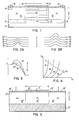
- FIG. 1 An example of a field effect transistor (FET) structure according to the invention is given in Fig. 1 in schematic representation.
- a substrate 10 for example, a suitably doped p-type silicon wafer, forms the body of the FET.
- p and p+ silicon are deposited to form a p region in which a p+ layer is buried as the process progresses.
- the buried layer 16 may be formed, for example, by ion implantation from the upper surface 18 of a silicon wafer with appropriate energy and dosage of boron.
- the buried layer 16 is arranged to underlie the channel 20 of the FET, which channel is defined by the distance between the depth diffused or implanted n+ source-22 and drain-24 regions, the latter of which have electrodes 26 and 28 respectively attached.
- the depth of the buried layer is not overly critical, a depth of a few thousand angstroms is sufficient.
- the buried layer 16 is to form a high barrier between the source and drain and restrict the current flow to the channel region 20.
- the region below the gate and above the p+ implant remains much as in the original substrate from which it was formed.
- An insulated layer 30, such as Si02, is thermally grown on the upper surface 18 above which a gate electrode 32 is arranged.
- the channel region 20 of length L between the source and drain is appropriately doped p-type such that the n+ doped source and drain depletion regions overlap, but the overlapped region is such that in the absence of the gate field it has a potential barrier for electrons high enough to prevent the injection of electrons for channel conduction.
- the actual barrier height potential in the absence of the applied field is determined by the channel doping and channel length L.
- the O profile 18' is at the interface between the channel and the gate oxide.
- the numbers 0-4 depict relative depth into the channel measured from the interface.
- the source-drain voltage introduces a longitudinal field which also- modulates and distorts the barrier such as shown in Fig. 3.
- the parameters 54, 56 and 58 associated with each potential profile depict the distances from the oxide-Si interface 18 into the channel 20, in that order. Here a positive gate voltage is applied.
- the emission limited current is a strong function of the barrier height, ⁇ , 0 ⁇ f-exp (- ⁇ I>s/kT) ⁇ .
- ⁇ B /kT decreases due to the applied gate potential, space charge in the channel will limit the current.
- the space charge limited current is a strong function of the drain voltage V d and channel length L ⁇ V d 2 L -3 in case of scattering limited, and ⁇ V D 3/2 L -2 in case of ballistic transport for an extremely short channel where channel length is smaller than the mean free path.
- a new class of device is realized, one whose transfer I-E characteristics are shown schematically in Fig. 4 with considerably larger current gain than the conventional inversion layer FET, especially for a small channel length L.
- the depth of the channel is controlled by a buried p+ region 16 shown in Fig. 1 beneath the desired channel depth that it is desired to modulate.
- the p+ region 16 will be a high barrier for electrons between the source and drain regions, thus stopping an undesirable parasitic current flow.
- FIG. 5 An alternative structure in accordance with the invention is shown in Fig. 5, again in schematic representation.
- an insulating substrate 10' is provided preferably of sapphire. Silicon regions 20', 22' and 24' are deposited on the sapphire substrate in well known manner used in fabricating Silicon-On-Sapphire (SOS) transistors.
- SOS Silicon-On-Sapphire
- the essential structure has a channel region 20' of one conductivity type, p- as shown for example, and source and drain regions of the opposite conductivity, n+ as shown in the example.
- the channel region has a length L less than twice the depletion width of the source and drain regions 22' and 24'.
- the insulating substrate 10' performs the function of the buried layer 16 in the previously described embodiment. Current is thus restricted to the channel region 20.
- the channel width may be shorter than the mean free path of the conduction carriers whereby the FET operates in a ballistic region wherein the electron velocity exceeds the saturation velocity resulting from energy loss to the
Landscapes
- Junction Field-Effect Transistors (AREA)
Claims (5)
Applications Claiming Priority (2)
| Application Number | Priority Date | Filing Date | Title |
|---|---|---|---|
| US20303780A | 1980-11-03 | 1980-11-03 | |
| US203037 | 1980-11-03 |
Publications (3)
| Publication Number | Publication Date |
|---|---|
| EP0051134A2 EP0051134A2 (de) | 1982-05-12 |
| EP0051134A3 EP0051134A3 (en) | 1982-12-08 |
| EP0051134B1 true EP0051134B1 (de) | 1986-01-08 |
Family
ID=22752203
Family Applications (1)
| Application Number | Title | Priority Date | Filing Date |
|---|---|---|---|
| EP81107091A Expired EP0051134B1 (de) | 1980-11-03 | 1981-09-09 | Feldeffekttransistor Schaltkreisanordnung |
Country Status (4)
| Country | Link |
|---|---|
| EP (1) | EP0051134B1 (de) |
| JP (1) | JPS5796571A (de) |
| CA (1) | CA1163729A (de) |
| DE (1) | DE3173446D1 (de) |
Families Citing this family (1)
| Publication number | Priority date | Publication date | Assignee | Title |
|---|---|---|---|---|
| US4937640A (en) * | 1980-11-03 | 1990-06-26 | International Business Machines Corporation | Short channel MOSFET |
Family Cites Families (4)
| Publication number | Priority date | Publication date | Assignee | Title |
|---|---|---|---|---|
| US3946419A (en) * | 1973-06-27 | 1976-03-23 | International Business Machines Corporation | Field effect transistor structure for minimizing parasitic inversion and process for fabricating |
| JPS5226177A (en) * | 1975-08-25 | 1977-02-26 | Toshiba Corp | Semi-conductor unit |
| JPS5370768A (en) * | 1976-12-07 | 1978-06-23 | Fujitsu Ltd | Integrated circuit |
| JPS559452A (en) * | 1978-07-05 | 1980-01-23 | Nec Corp | Short channel mis type electric field effective transistor |
-
1981
- 1981-09-09 EP EP81107091A patent/EP0051134B1/de not_active Expired
- 1981-09-09 DE DE8181107091T patent/DE3173446D1/de not_active Expired
- 1981-09-25 CA CA000386686A patent/CA1163729A/en not_active Expired
- 1981-10-16 JP JP56164345A patent/JPS5796571A/ja active Granted
Also Published As
| Publication number | Publication date |
|---|---|
| JPH0261157B2 (de) | 1990-12-19 |
| EP0051134A3 (en) | 1982-12-08 |
| CA1163729A (en) | 1984-03-13 |
| JPS5796571A (en) | 1982-06-15 |
| DE3173446D1 (en) | 1986-02-20 |
| EP0051134A2 (de) | 1982-05-12 |
Similar Documents
| Publication | Publication Date | Title |
|---|---|---|
| US5923987A (en) | Method for forming MOS devices with retrograde pocket regions and counter dopant regions at the substrate surface | |
| US6313487B1 (en) | Vertical channel floating gate transistor having silicon germanium channel layer | |
| US4819043A (en) | MOSFET with reduced short channel effect | |
| US6576966B1 (en) | Field-effect transistor having multi-part channel | |
| US6093951A (en) | MOS devices with retrograde pocket regions | |
| US5825049A (en) | Resonant tunneling device with two-dimensional quantum well emitter and base layers | |
| US5185280A (en) | Method of fabricating a soi transistor with pocket implant and body-to-source (bts) contact | |
| US6110783A (en) | Method for forming a notched gate oxide asymmetric MOS device | |
| US5650340A (en) | Method of making asymmetric low power MOS devices | |
| US6121666A (en) | Split gate oxide asymmetric MOS devices | |
| KR100460553B1 (ko) | 절연 게이트형 반도체 장치 제조 방법 | |
| US5985727A (en) | Method for forming MOS devices with retrograde pocket regions and counter dopant regions buried in the substrate surface | |
| JP4014677B2 (ja) | 絶縁ゲイト型半導体装置 | |
| EP0181091B1 (de) | Feldeffekttransistor mit einem Schottky-Gate und Herstellungsverfahren dafür | |
| KR910000929B1 (ko) | 금속 산화물 반도체 전계 효과 트랜지스터 | |
| JPH08181314A (ja) | 低閾値電圧mosトランジスタおよびその製造方法 | |
| KR19990082088A (ko) | 드레인 전계 종결 영역을 구비하는 단채널 페르미-문턱 전계 효과 트랜지스터 및 그 제조 방법 | |
| JPH05145083A (ja) | 量子電界効果素子 | |
| JP3949193B2 (ja) | 絶縁ゲイト型半導体装置 | |
| KR100443437B1 (ko) | 절연게이트형반도체장치및그제작방법 | |
| WO1988003328A1 (en) | Striped-channel transistor and method of forming the same | |
| JPH08236758A (ja) | 非対称mosデバイスおよびその製造方法 | |
| EP0051134B1 (de) | Feldeffekttransistor Schaltkreisanordnung | |
| JP2897736B2 (ja) | 化合物半導体電界効果トランジスタ | |
| JPS60247974A (ja) | 半導体装置 |
Legal Events
| Date | Code | Title | Description |
|---|---|---|---|
| PUAI | Public reference made under article 153(3) epc to a published international application that has entered the european phase |
Free format text: ORIGINAL CODE: 0009012 |
|
| 17P | Request for examination filed |
Effective date: 19810909 |
|
| AK | Designated contracting states |
Designated state(s): DE FR GB IT |
|
| PUAL | Search report despatched |
Free format text: ORIGINAL CODE: 0009013 |
|
| AK | Designated contracting states |
Designated state(s): DE FR GB IT |
|
| GRAA | (expected) grant |
Free format text: ORIGINAL CODE: 0009210 |
|
| AK | Designated contracting states |
Designated state(s): DE FR GB IT |
|
| REF | Corresponds to: |
Ref document number: 3173446 Country of ref document: DE Date of ref document: 19860220 |
|
| ITF | It: translation for a ep patent filed | ||
| ET | Fr: translation filed | ||
| PLBE | No opposition filed within time limit |
Free format text: ORIGINAL CODE: 0009261 |
|
| STAA | Information on the status of an ep patent application or granted ep patent |
Free format text: STATUS: NO OPPOSITION FILED WITHIN TIME LIMIT |
|
| 26N | No opposition filed | ||
| PGFP | Annual fee paid to national office [announced via postgrant information from national office to epo] |
Ref country code: DE Payment date: 19910926 Year of fee payment: 11 |
|
| ITTA | It: last paid annual fee | ||
| PGFP | Annual fee paid to national office [announced via postgrant information from national office to epo] |
Ref country code: GB Payment date: 19920824 Year of fee payment: 12 |
|
| PGFP | Annual fee paid to national office [announced via postgrant information from national office to epo] |
Ref country code: FR Payment date: 19920904 Year of fee payment: 12 |
|
| PG25 | Lapsed in a contracting state [announced via postgrant information from national office to epo] |
Ref country code: DE Effective date: 19930602 |
|
| PG25 | Lapsed in a contracting state [announced via postgrant information from national office to epo] |
Ref country code: GB Effective date: 19930909 |
|
| GBPC | Gb: european patent ceased through non-payment of renewal fee |
Effective date: 19930909 |
|
| PG25 | Lapsed in a contracting state [announced via postgrant information from national office to epo] |
Ref country code: FR Free format text: LAPSE BECAUSE OF NON-PAYMENT OF DUE FEES Effective date: 19940531 |
|
| REG | Reference to a national code |
Ref country code: FR Ref legal event code: ST |