EP0053483A2 - Méthode de fabrication d'un module pour une liaison par fibres optiques - Google Patents
Méthode de fabrication d'un module pour une liaison par fibres optiques Download PDFInfo
- Publication number
- EP0053483A2 EP0053483A2 EP81305591A EP81305591A EP0053483A2 EP 0053483 A2 EP0053483 A2 EP 0053483A2 EP 81305591 A EP81305591 A EP 81305591A EP 81305591 A EP81305591 A EP 81305591A EP 0053483 A2 EP0053483 A2 EP 0053483A2
- Authority
- EP
- European Patent Office
- Prior art keywords
- dies
- module
- cavity
- unit
- case
- Prior art date
- Legal status (The legal status is an assumption and is not a legal conclusion. Google has not performed a legal analysis and makes no representation as to the accuracy of the status listed.)
- Granted
Links
Images


Classifications
-
- G—PHYSICS
- G02—OPTICS
- G02B—OPTICAL ELEMENTS, SYSTEMS OR APPARATUS
- G02B6/00—Light guides; Structural details of arrangements comprising light guides and other optical elements, e.g. couplings
- G02B6/24—Coupling light guides
- G02B6/42—Coupling light guides with opto-electronic elements
- G02B6/4292—Coupling light guides with opto-electronic elements the light guide being disconnectable from the opto-electronic element, e.g. mutually self aligning arrangements
-
- H—ELECTRICITY
- H10—SEMICONDUCTOR DEVICES; ELECTRIC SOLID-STATE DEVICES NOT OTHERWISE PROVIDED FOR
- H10H—INORGANIC LIGHT-EMITTING SEMICONDUCTOR DEVICES HAVING POTENTIAL BARRIERS
- H10H20/00—Individual inorganic light-emitting semiconductor devices having potential barriers, e.g. light-emitting diodes [LED]
- H10H20/80—Constructional details
- H10H20/85—Packages
- H10H20/8506—Containers
-
- H—ELECTRICITY
- H10—SEMICONDUCTOR DEVICES; ELECTRIC SOLID-STATE DEVICES NOT OTHERWISE PROVIDED FOR
- H10W—GENERIC PACKAGES, INTERCONNECTIONS, CONNECTORS OR OTHER CONSTRUCTIONAL DETAILS OF DEVICES COVERED BY CLASS H10
- H10W90/00—Package configurations
- H10W90/701—Package configurations characterised by the relative positions of pads or connectors relative to package parts
- H10W90/751—Package configurations characterised by the relative positions of pads or connectors relative to package parts of bond wires
- H10W90/756—Package configurations characterised by the relative positions of pads or connectors relative to package parts of bond wires between a chip and a stacked lead frame, conducting package substrate or heat sink
-
- Y—GENERAL TAGGING OF NEW TECHNOLOGICAL DEVELOPMENTS; GENERAL TAGGING OF CROSS-SECTIONAL TECHNOLOGIES SPANNING OVER SEVERAL SECTIONS OF THE IPC; TECHNICAL SUBJECTS COVERED BY FORMER USPC CROSS-REFERENCE ART COLLECTIONS [XRACs] AND DIGESTS
- Y10—TECHNICAL SUBJECTS COVERED BY FORMER USPC
- Y10S—TECHNICAL SUBJECTS COVERED BY FORMER USPC CROSS-REFERENCE ART COLLECTIONS [XRACs] AND DIGESTS
- Y10S359/00—Optical: systems and elements
- Y10S359/90—Methods
Definitions
- the present invention relates to a method for manufacturing a module for a fiber optic link and, more particularly, to a method for manufacturing a transmitter and receiver module for a fiber optic link.
- an optical signal generated in a transmission module is guided to an optical fiber cable, is transmitted through the fiber cable, and is detected in a receiver module to be converted into an electric signal.
- optical communication between the fiber cable and the receiver and transmitter modules, that is, the modules is important.
- the optical axis of an optoelectronic element in a module that is, a photodiode in the receiver module or an LED (Light Emitting Diode) in the transmitter module, be aligned with the optical axis at the end face of the optical fiber of the fiber cable in a precise manner, for example, within an error allowance of several to several tens of microns.
- the present invention provides a method for manufacturing a module for a fiber optic link comprising the steps of:
- Fig. 1 shows the receiver side of a fiber optic link.
- the receiver side includes an optical fiber cable 2, a connector 4 fixed to one end of the fiber cable 2, and a module (receiver module) 6 to which is mounted the connector 4.
- the transmitter side of the fiber optic link is of substantially the same structure as that of the receiver side.
- the internal structure of the module is also the same for both the transmitter and receiver sides except for the circuit elements and the optoelectronic element assembled in each module. Therefore, although the description will be made only with reference to the module, it is to be understood that the module refers both to the receiver module and the transmitter module.
- the optical fiber cable 2 is obtained in a generally known method by covering a glass or plastic optical fiber 8 comprising of a core and a cladding with a flexible light-shielding material.
- the connector 4 is manufactured by injection molding. As shown in Fig. 2, the optical fiber cable 2 is fixed to a fixing section 10 of the connector 4.
- the optical fiber cable 2 further extends inside a cylindrical rigid plug 14 coaxially projecting from the fixing section 10 and terminates at the front end of the plug 14.
- a snap piece 16 is arranged inside a knurled section 12.
- a cylindrical socket 18 projects from a main body case 20 to correspond with the cylindrical rigid plug 14.
- the inner diameter of the socket 18 is set to be substantially equal to or slightly greater than the outer diameter of the plug 14.
- the outer diameter of the socket 18 is also set to be slightly greater than a distance between projections of the snap piece 16 facing each other.
- a stepped section 22 is formed at the socket 18 so as to engage with the snap piece of the connector 4 when the connector 4 is mounted to the socket 18.
- the hole 19 of the socket 18 in which is inserted the plug 14 communicates with a space 23 which extends inside the main body case 20 and which houses a circuit unit 24.
- the receiver module 6 is manufactured by injection molding as in the case of the connector 4.
- the circuit unit 24 is manufactured by transfer molding.
- the receiver module 6 and the connector 4 are made of a light-shielding material which does not transmit light, while the circuit unit 24 is made of a transparent resin.
- the circuit unit 24 within the circuit unit 24 are embedded five Ag-plated lead frames 26-1, 26-2, 26-3, 26-4 and 26-5.
- the lead frame 26-5 extends to and terminates at one side of the unit 24, while the other lead frames 26-1, 26-2, 26-3 and 26-4 extend to the outside the unit 24 at the other side and terminate into pins 28-1, 28-2, 28-3 and 28-4.
- On the lead frame 26-1 is mounted through a conductive paste an optoelectronic element 30, an LED pellet in the case of the transmitter module and a photodiode in the case of the receiver module.
- the bonding pads of the optoelectronic element 30, the IC chip 32 and the lead frames 26-1, 26-2, 26-3, 26-4, and 26-5 are electrically connected through gold bonding wires 34.
- the optoelectronic element 30 is embedded at a predetermined position of the unit 24 so that the optoelectronic element 30 opposes at a distance the hole 19 of the socket 18 and is aligned with the central axis of the hole 19, when the end of the circuit unit 24 is mounted within the main body case 20.
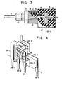
- a convex lens segment 36 is formed at the region of the unit 24 where the optoelectronic element 30 is embedded, as shown in Fig. 3.
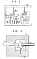
- a copper plate is punched into a desired shape and is Ag-plated to provide a frame 40 as shown in Fig. 5.
- the IC chip 32 and the optoelectronic element 30, that is, the LED or the photodiode, are mounted on the lead frames 26-1 and 26-2 with a conductive paste to be electrically connected thereto.
- the optoelectronic element 30 is connected to the lead frame 26-5 with a gold bonding wire having a diameter of 25 ⁇ m.
- the bonding pads of the IC chip 32 are respectively connected to the lead frames 26-2, 26-3, 26-4, and 26-5 with the bonding wires.
- the frame 40 with the IC chip 32 and the optoelectric element 30 is mounted in a pair of dies (not shown) having a cavity of a predetermined contour.
- a transparent thermosetting resin for example, a transparent thermosetting epoxy resin MP-8500 manufactured by Nitto Denshi-kogyo K.K., under certain conditions, 0 for example, at a temperature of 160 C and a pressure of 30 kg/cm 2 .
- the unit 24 as shown in Fig. 3 is transfer molded.
- the unit 24 obtained by the transfer molding in this manner is embeded in the case 20 which is obtained by injection molding.
- the unit 24 is clamped between a first die rod 42 and a second die rod 44.
- the first die rod 42 has an outer diameter substantially equal to the inner diameter of the hole 19 and has, at its front end, a recess conforming to the shape of the front part of the unit 24, as shown in Fig. 6.
- the optical axis of the optoelectric element 30 and the lens segment 36 is aligned with the central axis of the die 42.
- a pair of dies 46 and 48 are attached to define therebetween a cavity 50, which corresponds to the shape of the case 20.
- the die rods 42 and 44 and the dies 46 and 48 are kept at a temperature lower than a constant temperature, for example, 80°C.
- a black thermosetting epoxy resin EME-155F manufactured by Sumitomo Bakelite K.K. under certain condition, for example, at a temperature of 165°C and a pressure of 80 kg/cm.
- the resin is cured, the die rods 42 and 44 are removed and the dies 46 and 48 are withdrawn.
- a cap 52 for shielding light from outside is covered over the hole 23 formed in the case 20 to complete the module as shown in Figs. 1 and 3.
- the optical axis of the optoelectronic element 30 and the lens segment 36 of the unit 24 is aligned with the central axis of the die rod 42 in advance, the optoelectronic element 30 and the lens segment 36 are correctly aligned with the hole 19 of the socket 18 and the case 20 of the completed module 6.
- the unit 24 is obtained by transfer molding. Therefore, during the manufacture of the unit 24, the bonding wires 34 may not be disconnected with the material to be transfer molded, and the optoelectronic element 30 and the IC chip 32 may not be distorted very much.
- the case 20 is obtained by injection molding. Therefore, the case 20 is manufactured with high precision, so that the abrasion resistance and mechanical strength of the case may be improved. Furthermore, according to the injection molding process, the curing time of the molding material can be shortened. Therefore, even when the die rod 42 as shown in Fig. 6 is used, the introduction of the molding material into a space between the surface of the lens segment 36 of the module 24 and the front end surface of the die rod 42 may be prevented and the covering of the surface of the lens segment 36 with the light-shielding material may be prevented.
- the module 6 may be made small in size, and the time required for manufacturing it may be shortened. Moreover, since the central axis of the hole 19 of the module 6 is correctly aligned with the optical axis of the optoelectronic element 30 and the lens segment 36, the fiber cable 2 may be correctly optically coupled with the optoelectronic element 30 by only coupling the fiber cable 2 with the module 6 through the connector 4.
- the end of the unit 24 is embedded in the case 20.
- the unit 24 be formed in the space or hole 23 at a distance from the inner surface of the case 20, depending upon the molding conditions of the case 20. If part of the surface of the unit 24 is brought into contact with the molding material for injection molding as in the case of Fig. 3, the surface of the unit 24 may be subjected to a high temperature and a high pressure during injection molding, and the unit 24 may be damaged by the mechanical force or heat and the characteristics may change.
- the die rod 42 has a recess which receives not only the front end surface but the front part of the unit 24, and the die rod 44 has a recess which receives the rear part of the unit 24.
- the case 20 is injection molded under the condition that the unit 24 is positioned in the cavity defined by these die rods 42 and 44. In this case, even when the unit 24 is subjected to the mechanical force or heat during injection molding, the unit 24 is protected by the die rods 42 and 44, and the IC chip 32 and the optoelectronic element 30 are protected.
- the transparent unit 24 is supported in the case 20 by the lead frame to maintain a distance between the module 24 and the case 20.
- a ring-shaped spacer 54 of a heat-insulating material such as ceramic or resin may be arranged between the inner surface of the case 20 and the surface of the front part of the unit 24.
- the ring-shaped spacer 54 is fitted at the front end of the die rod 42 as shown in Fig. 10.
- the unit 24 is clamped between this spacer 54 and the die rod 44, and the unit 24 is fitted with the spacer 54 so that the optical axis of the lens segment 36 and the optoelectronic element 30 is aligned with the central axis of the die rod 42. According to this method, the unit 24 is clamped through the spacer 54 and the spacer 54 remains inside the case 20. Therefore, even when the size of the unit 24 is made greater, the unit 24 may be correctly aligned by only preparing the spacer of a shape conforming to the front part of the unit 24.
- the outer diameter of the die rod 42 is determined by the outer diameter of the plug 14. Since the die rod 42 is withdrawn after the molding, the front end of it may not be made larger. However, if the spacer 54 is used, the positioning of the unit 24 may be correctly accomplished while the size of the unit 24 may be made greater. If the size of the unit 24 may be made greater, the size of the frame 40 and the arrangement of the optoelectronic element 30 and the IC chip 32 inside the unit 24 may be more freely selected, so that the manufacture of the unit 24 is facilitated and mass production of it is also facilitated.
- the optoelectric element such as an LED or a photodiode and the peripheral circuits formed into an IC chip is embedded in a molded body or unit.
- the case is manufactured in correspondence with this molded body. Therefore, correct alignment may be achieved by simply connecting the fiber optic cable to the module through the connector. Since this manufacturing method is suitable for mass production, the unit price of the module may be reduced.
Landscapes
- Physics & Mathematics (AREA)
- General Physics & Mathematics (AREA)
- Optics & Photonics (AREA)
- Optical Couplings Of Light Guides (AREA)
Applications Claiming Priority (4)
| Application Number | Priority Date | Filing Date | Title |
|---|---|---|---|
| JP166686/80 | 1980-11-28 | ||
| JP166687/80 | 1980-11-28 | ||
| JP55166686A JPS6052600B2 (ja) | 1980-11-28 | 1980-11-28 | 光モジユ−ルの製造方法 |
| JP16668780A JPS5791572A (en) | 1980-11-28 | 1980-11-28 | Light module and manufacture therefor |
Publications (3)
| Publication Number | Publication Date |
|---|---|
| EP0053483A2 true EP0053483A2 (fr) | 1982-06-09 |
| EP0053483A3 EP0053483A3 (en) | 1983-03-09 |
| EP0053483B1 EP0053483B1 (fr) | 1985-10-02 |
Family
ID=26490966
Family Applications (1)
| Application Number | Title | Priority Date | Filing Date |
|---|---|---|---|
| EP81305591A Expired EP0053483B1 (fr) | 1980-11-28 | 1981-11-26 | Méthode de fabrication d'un module pour une liaison par fibres optiques |
Country Status (3)
| Country | Link |
|---|---|
| US (1) | US4410469A (fr) |
| EP (1) | EP0053483B1 (fr) |
| DE (1) | DE3172553D1 (fr) |
Cited By (6)
| Publication number | Priority date | Publication date | Assignee | Title |
|---|---|---|---|---|
| EP0419875A3 (en) * | 1989-09-29 | 1992-07-08 | Sumitomo Electric Industries, Ltd. | Light communication apparatus |
| EP0446410A3 (en) * | 1990-03-13 | 1992-11-19 | Sumitomo Electric Industries, Ltd. | Optical module and process of producing the same |
| EP0635741A3 (fr) * | 1993-07-19 | 1996-01-10 | Motorola Inc | Interface optoélectronique et procédé de sa fabrication. |
| EP0921426A1 (fr) * | 1997-12-03 | 1999-06-09 | Sumitomo Electric Industries, Ltd. | Liaiso des données optiques |
| US6869232B2 (en) | 2002-03-08 | 2005-03-22 | Infineon Technologies Ag | Receiving and coupling part for opto-electronic transmission and/or reception element |
| WO2009028159A1 (fr) * | 2007-08-24 | 2009-03-05 | Yazaki Corporation | Composant semi-conducteur optique intégré dans un boîtier et son procédé de fabrication |
Families Citing this family (44)
| Publication number | Priority date | Publication date | Assignee | Title |
|---|---|---|---|---|
| US4689005A (en) * | 1982-11-02 | 1987-08-25 | Polaroid Corporation | Molding apparatus |
| US4531702A (en) * | 1982-11-02 | 1985-07-30 | Polaroid Corporation | Injection mold for forming optical fiber connector |
| US4689184A (en) * | 1982-11-02 | 1987-08-25 | Polaroid Corporation | Method for forming an optical connector |
| US4690492A (en) * | 1984-09-04 | 1987-09-01 | Oximetrix, Inc. | Optical coupling |
| US5098630A (en) * | 1985-03-08 | 1992-03-24 | Olympus Optical Co., Ltd. | Method of molding a solid state image pickup device |
| JPS61157910U (fr) * | 1985-03-23 | 1986-09-30 | ||
| US4935581A (en) * | 1986-04-17 | 1990-06-19 | Citizen Watch Co., Ltd. | Pin grid array package |
| JPS62244139A (ja) * | 1986-04-17 | 1987-10-24 | Citizen Watch Co Ltd | 樹脂封止型ピングリツドアレイ及びその製造方法 |
| USD314176S (en) | 1987-09-30 | 1991-01-29 | Hewlett-Packard Company | Fiber optic component |
| US5013495A (en) * | 1988-02-05 | 1991-05-07 | Tokai Rubber Industries, Ltd. | Method of producing optical fiber connectors |
| CA2036727C (fr) * | 1990-03-13 | 1998-12-22 | Hisao Go | Module optique avec prise de raccordement et methode de production dudit module |
| US5149958A (en) * | 1990-12-12 | 1992-09-22 | Eastman Kodak Company | Optoelectronic device component package |
| US5275765A (en) * | 1991-01-23 | 1994-01-04 | Sumitomo Electric Industries, Ltd. | Method of manufacturing an optical module using a mold die |
| US5113466A (en) * | 1991-04-25 | 1992-05-12 | At&T Bell Laboratories | Molded optical packaging arrangement |
| US5123066A (en) * | 1991-04-25 | 1992-06-16 | At&T Bell Laboratories | Molded optical package utilizing leadframe technology |
| US5337398A (en) * | 1992-11-30 | 1994-08-09 | At&T Bell Laboratories | Single in-line optical package |
| US5313545A (en) * | 1993-02-19 | 1994-05-17 | Motorola, Inc. | Molded waveguide with a unitary cladding region and method of making |
| US5328552A (en) * | 1993-03-30 | 1994-07-12 | At&T Bell Laboratories | Leadframe processing for molded package arrangements |
| US5482658A (en) * | 1993-08-13 | 1996-01-09 | Motorola, Inc. | Method of making an optoelectronic interface module |
| US5475783A (en) * | 1993-09-30 | 1995-12-12 | Sumitomo Electric Industries, Ltd. | Optical module, method of manufacturing the same, and sleeve |
| SE9403574L (sv) * | 1994-10-19 | 1996-04-20 | Ericsson Telefon Ab L M | Optokomponentkapsel med optiskt gränssnitt |
| CA2161718A1 (fr) * | 1994-10-31 | 1996-05-01 | Hiromi Kurashima | Module optique a structure permettant de determiner la position des manchons par rapport a celle des porte-manchons |
| US6354747B1 (en) | 1996-08-26 | 2002-03-12 | Sumitomo Electric Industries, Ltd. | Optical module |
| DE69723630T2 (de) * | 1996-08-26 | 2004-04-15 | Sumitomo Electric Industries, Ltd. | Optoelektronisches Modul und Verfahren zu dessen Herstellung |
| DE19711138C2 (de) * | 1997-03-07 | 1998-12-17 | Siemens Ag | Herstellungsverfahren für ein elektrooptisches Modul |
| JP4090512B2 (ja) * | 1997-04-08 | 2008-05-28 | 日本オプネクスト株式会社 | 光モジュール |
| US6239427B1 (en) | 1998-01-14 | 2001-05-29 | Sumitomo Electric Industries, Ltd. | Optical data link |
| US6901221B1 (en) | 1999-05-27 | 2005-05-31 | Jds Uniphase Corporation | Method and apparatus for improved optical elements for vertical PCB fiber optic modules |
| US6213651B1 (en) | 1999-05-26 | 2001-04-10 | E20 Communications, Inc. | Method and apparatus for vertical board construction of fiber optic transmitters, receivers and transceivers |
| US6793863B1 (en) * | 1999-06-15 | 2004-09-21 | Lexington Insulators | Process for producing a spark plug boot resistor assembly |
| JP2001108870A (ja) * | 1999-10-06 | 2001-04-20 | Mitsubishi Electric Corp | 光デバイス及びその製造方法 |
| DE10004411A1 (de) * | 2000-02-02 | 2001-08-16 | Infineon Technologies Ag | Elektrooptisches Sende-/Empfangsmodul und Verfahren zu seiner Herstellung |
| DE10043483A1 (de) * | 2000-09-04 | 2002-07-25 | Infineon Technologies Ag | Optisches Sendemodul |
| DE10227544B4 (de) * | 2002-06-17 | 2007-08-02 | Infineon Technologies Ag | Vorrichtung zur optischen Datenübertragung |
| US6913398B2 (en) * | 2002-08-12 | 2005-07-05 | Oxford Diffraction Ltd | Frame for a fiber optic taper |
| US8048358B2 (en) * | 2006-04-18 | 2011-11-01 | Texas Instruments Incorporated | Pop semiconductor device manufacturing method |
| US8218917B2 (en) * | 2007-03-09 | 2012-07-10 | Omron Corporation | Package manufacturing method, package, optical module and die for integral molding |
| US7745898B2 (en) * | 2007-12-20 | 2010-06-29 | International Business Machines Corporation | Multichip package, methods of manufacture thereof and articles comprising the same |
| JP2009253166A (ja) * | 2008-04-09 | 2009-10-29 | Yazaki Corp | 光通信モジュール |
| ES2703235T3 (es) | 2011-11-23 | 2019-03-07 | Adc Telecommunications Inc | Conector de fibra óptica multi-fibra |
| CN104364686B (zh) | 2012-02-07 | 2016-11-16 | 泰科电子瑞侃有限公司 | 用于连接器的线缆端接组件和方法 |
| CA2864886A1 (fr) | 2012-02-20 | 2013-08-29 | Adc Telecommunications, Inc. | Connecteur de fibre optique, ensemble connecteur de fibre optique et cable a fibres optiques, et methodes de fabrication |
| US8939654B2 (en) | 2012-09-27 | 2015-01-27 | Adc Telecommunications, Inc. | Ruggedized multi-fiber fiber optic connector with sealed dust cap |
| US9720185B2 (en) | 2014-05-23 | 2017-08-01 | Commscope Technologies Llc | Systems and method for processing optical cable assemblies |
Family Cites Families (16)
| Publication number | Priority date | Publication date | Assignee | Title |
|---|---|---|---|---|
| DE1082983B (de) | 1959-04-30 | 1960-06-09 | Siemens Ag | Verfahren zur Herstellung von kunststoffumpressten Trockengleichrichteranordnungen und Pressform zur Durchfuehrung des Verfahrens |
| NL6812451A (fr) * | 1968-08-31 | 1970-03-03 | ||
| US3660669A (en) * | 1970-04-15 | 1972-05-02 | Motorola Inc | Optical coupler made by juxtaposition of lead frame mounted sensor and light emitter |
| US3715423A (en) * | 1971-01-25 | 1973-02-06 | Motorola Inc | Plastic encapsulation of semiconductor devices |
| US3972663A (en) * | 1973-01-22 | 1976-08-03 | Toko Incorporated | Method and apparatus for packaging electronic components with thermosetting material |
| US3981074A (en) * | 1974-08-23 | 1976-09-21 | Nitto Electric Industrial Co., Ltd. | Method for producing plastic base caps for split cavity type package semi-conductor units |
| CA1065140A (fr) * | 1975-06-05 | 1979-10-30 | Thomas R. Kyle | Methode de scellement de fibres optiques a un dispositif d'encapsulation |
| JPS5229749A (en) * | 1975-09-02 | 1977-03-05 | Mitsubishi Electric Corp | Optical equipment and its manufacturing process |
| US4216577A (en) * | 1975-12-31 | 1980-08-12 | Compagnie Internationale Pour L'informatique Cii-Honeywell Bull (Societe Anonyme) | Portable standardized card adapted to provide access to a system for processing electrical signals and a method of manufacturing such a card |
| US4084882A (en) * | 1976-08-30 | 1978-04-18 | International Telephone And Telegraph Corporation | Connector member |
| US4173389A (en) * | 1977-09-28 | 1979-11-06 | Bell Telephone Laboratories, Incorporated | Molded optical fiber connector |
| US4188708A (en) * | 1977-10-03 | 1980-02-19 | National Semiconductor Corporation | Integrated circuit package with optical input coupler |
| JPS5841661B2 (ja) * | 1978-05-16 | 1983-09-13 | オムロン株式会社 | 樹脂封止形半導体装置の製造方法 |
| US4186996A (en) * | 1978-09-22 | 1980-02-05 | Amp Incorporated | Optic adaptor junction |
| JPS55129307A (en) * | 1979-02-06 | 1980-10-07 | Texas Instruments Inc | Self matching fiberroptical package |
| US4305204A (en) * | 1980-01-16 | 1981-12-15 | Litronix, Inc. | Method for making display device |
-
1981
- 1981-11-26 DE DE8181305591T patent/DE3172553D1/de not_active Expired
- 1981-11-26 EP EP81305591A patent/EP0053483B1/fr not_active Expired
- 1981-11-27 US US06/325,486 patent/US4410469A/en not_active Expired - Lifetime
Cited By (9)
| Publication number | Priority date | Publication date | Assignee | Title |
|---|---|---|---|---|
| EP0419875A3 (en) * | 1989-09-29 | 1992-07-08 | Sumitomo Electric Industries, Ltd. | Light communication apparatus |
| EP0446410A3 (en) * | 1990-03-13 | 1992-11-19 | Sumitomo Electric Industries, Ltd. | Optical module and process of producing the same |
| EP0635741A3 (fr) * | 1993-07-19 | 1996-01-10 | Motorola Inc | Interface optoélectronique et procédé de sa fabrication. |
| EP0921426A1 (fr) * | 1997-12-03 | 1999-06-09 | Sumitomo Electric Industries, Ltd. | Liaiso des données optiques |
| US6234686B1 (en) | 1997-12-03 | 2001-05-22 | Sumitomo Electric Industries, Ltd. | Optical data link |
| US6869232B2 (en) | 2002-03-08 | 2005-03-22 | Infineon Technologies Ag | Receiving and coupling part for opto-electronic transmission and/or reception element |
| EP1483613B1 (fr) * | 2002-03-08 | 2011-10-12 | Avago Technologies Fiber IP (Singapore) Pte. Ltd. | Partie de reception et de couplage pour un element emetteur optoelectronique |
| WO2009028159A1 (fr) * | 2007-08-24 | 2009-03-05 | Yazaki Corporation | Composant semi-conducteur optique intégré dans un boîtier et son procédé de fabrication |
| US8602661B2 (en) | 2007-08-24 | 2013-12-10 | Yazaki Corporation | Housing-integrated optical semiconductor component and manufacturing method thereof |
Also Published As
| Publication number | Publication date |
|---|---|
| EP0053483B1 (fr) | 1985-10-02 |
| US4410469A (en) | 1983-10-18 |
| DE3172553D1 (en) | 1985-11-07 |
| EP0053483A3 (en) | 1983-03-09 |
Similar Documents
| Publication | Publication Date | Title |
|---|---|---|
| EP0053483B1 (fr) | Méthode de fabrication d'un module pour une liaison par fibres optiques | |
| US4539476A (en) | Module for a fiber optic link | |
| EP0053482B1 (fr) | Module pour une connexion fiberoptique | |
| US5367593A (en) | Optical/electrical connector and method of fabrication | |
| JP4957503B2 (ja) | 光モジュールおよび光モジュールの製造方法 | |
| JP2513880B2 (ja) | 光学部品の製造方法 | |
| US4173389A (en) | Molded optical fiber connector | |
| KR100195850B1 (ko) | 광모듈과 그 제조 공정 | |
| AU653293B2 (en) | Transfer molding type manufacturing method of pigtail-type optical module | |
| US9869834B2 (en) | Photoelectric conversion connector and method for manufacturing same | |
| EP0446711B1 (fr) | Module optique comportant un récipient et procédé pour la fabrication de celui-ci | |
| US4740052A (en) | Connector for optical fiber | |
| EP0010352A1 (fr) | Dispositif semiconducteur optoélectronique | |
| US5500914A (en) | Optical interconnect unit and method or making | |
| US8602661B2 (en) | Housing-integrated optical semiconductor component and manufacturing method thereof | |
| US6877908B2 (en) | Fiber with ferrule, and optical module and method of manufacturing the same | |
| JP2973542B2 (ja) | 光モジュール及びその製造装置及びその製造方法 | |
| JPH02228617A (ja) | 光電変換モジュールの製造方法 | |
| JPH0638517B2 (ja) | 光モジュールの製造方法 | |
| JPH0772355A (ja) | 光電インターフェースおよびその製造方法 | |
| JP2864460B2 (ja) | 多心式光モジュール及びその製造方法 | |
| JPS6052600B2 (ja) | 光モジユ−ルの製造方法 | |
| JPH10123376A (ja) | 光データリンク及びその製造方法 | |
| JPS6244830B2 (fr) | ||
| JP2000105322A (ja) | 光部品用実装基板および光部品用実装基板の製造方法 |
Legal Events
| Date | Code | Title | Description |
|---|---|---|---|
| PUAI | Public reference made under article 153(3) epc to a published international application that has entered the european phase |
Free format text: ORIGINAL CODE: 0009012 |
|
| 17P | Request for examination filed |
Effective date: 19811202 |
|
| AK | Designated contracting states |
Designated state(s): DE FR GB |
|
| PUAL | Search report despatched |
Free format text: ORIGINAL CODE: 0009013 |
|
| AK | Designated contracting states |
Designated state(s): DE FR GB |
|
| RAP1 | Party data changed (applicant data changed or rights of an application transferred) |
Owner name: KABUSHIKI KAISHA TOSHIBA |
|
| GRAA | (expected) grant |
Free format text: ORIGINAL CODE: 0009210 |
|
| AK | Designated contracting states |
Designated state(s): DE FR GB |
|
| REF | Corresponds to: |
Ref document number: 3172553 Country of ref document: DE Date of ref document: 19851107 |
|
| ET | Fr: translation filed | ||
| PLBE | No opposition filed within time limit |
Free format text: ORIGINAL CODE: 0009261 |
|
| STAA | Information on the status of an ep patent application or granted ep patent |
Free format text: STATUS: NO OPPOSITION FILED WITHIN TIME LIMIT |
|
| 26N | No opposition filed | ||
| REG | Reference to a national code |
Ref country code: GB Ref legal event code: 746 Effective date: 19980917 |
|
| REG | Reference to a national code |
Ref country code: FR Ref legal event code: D6 |
|
| PGFP | Annual fee paid to national office [announced via postgrant information from national office to epo] |
Ref country code: FR Payment date: 20001110 Year of fee payment: 20 |
|
| PGFP | Annual fee paid to national office [announced via postgrant information from national office to epo] |
Ref country code: DE Payment date: 20001120 Year of fee payment: 20 |
|
| PGFP | Annual fee paid to national office [announced via postgrant information from national office to epo] |
Ref country code: GB Payment date: 20001122 Year of fee payment: 20 |
|
| PG25 | Lapsed in a contracting state [announced via postgrant information from national office to epo] |
Ref country code: GB Free format text: LAPSE BECAUSE OF EXPIRATION OF PROTECTION Effective date: 20011125 |
|
| REG | Reference to a national code |
Ref country code: GB Ref legal event code: PE20 Effective date: 20011125 |