EP0058577B1 - Halbleiteranordnung mit Elektronenablenkung vom Typ des "ballistischen Transportes" und Verfahren zum Herstellen einer solchen Anordnung - Google Patents
Halbleiteranordnung mit Elektronenablenkung vom Typ des "ballistischen Transportes" und Verfahren zum Herstellen einer solchen Anordnung Download PDFInfo
- Publication number
- EP0058577B1 EP0058577B1 EP82400033A EP82400033A EP0058577B1 EP 0058577 B1 EP0058577 B1 EP 0058577B1 EP 82400033 A EP82400033 A EP 82400033A EP 82400033 A EP82400033 A EP 82400033A EP 0058577 B1 EP0058577 B1 EP 0058577B1
- Authority
- EP
- European Patent Office
- Prior art keywords
- contacts
- layer
- row
- electrodes
- anode
- Prior art date
- Legal status (The legal status is an assumption and is not a legal conclusion. Google has not performed a legal analysis and makes no representation as to the accuracy of the status listed.)
- Expired
Links
Images


Classifications
-
- H—ELECTRICITY
- H10—SEMICONDUCTOR DEVICES; ELECTRIC SOLID-STATE DEVICES NOT OTHERWISE PROVIDED FOR
- H10D—INORGANIC ELECTRIC SEMICONDUCTOR DEVICES
- H10D30/00—Field-effect transistors [FET]
- H10D30/80—FETs having rectifying junction gate electrodes
- H10D30/87—FETs having Schottky gate electrodes, e.g. metal-semiconductor FETs [MESFET]
-
- H—ELECTRICITY
- H10—SEMICONDUCTOR DEVICES; ELECTRIC SOLID-STATE DEVICES NOT OTHERWISE PROVIDED FOR
- H10D—INORGANIC ELECTRIC SEMICONDUCTOR DEVICES
- H10D30/00—Field-effect transistors [FET]
-
- H—ELECTRICITY
- H10—SEMICONDUCTOR DEVICES; ELECTRIC SOLID-STATE DEVICES NOT OTHERWISE PROVIDED FOR
- H10D—INORGANIC ELECTRIC SEMICONDUCTOR DEVICES
- H10D30/00—Field-effect transistors [FET]
- H10D30/80—FETs having rectifying junction gate electrodes
- H10D30/87—FETs having Schottky gate electrodes, e.g. metal-semiconductor FETs [MESFET]
- H10D30/873—FETs having Schottky gate electrodes, e.g. metal-semiconductor FETs [MESFET] having multiple gate electrodes
Definitions
- the invention relates to a semiconductor device comprising a structure similar to that of field effect transistors of the “ballistic electron” type with which it is proposed to create, by new means, a deflection of “ballistic electrons so as to switch from ultra-fast a current or a signal or to phase out a signal in time.
- the invention also includes a method of manufacturing such a device.
- the electrons which move under the effect of an electric field in a semiconductor medium can carry out , over a distance of less than one micron, paths practically undisturbed in speed and direction by collisions with other particles.
- a semiconductor medium such as gallium arsenide, indium phosphide or the indium-antimony alloy
- These electrons are called ballistic.
- the travel time of the electrons, within a ballistic transport device, must be of the same order as the average time of relaxation of an electron between incidents leading to a loss of energy by any mechanism whatsoever in the semiconductor material .
- the invention aims to remedy these drawbacks by modifying the structure of the buried gate field-effect transistor fairly far enough to enable switches and phase shifters to be produced.
- the device of the invention there is a structure comprising at least one cathode, at least one anode, these two electrodes being located on either side of a semiconductor plate making it possible to observe the phenomenon of ballistic electrons and comprising a first buried gate electrode.
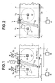
- the switching device shown in FIG. 1 comprises a strip 1 of semiconductor material (in partial section) which can for example be monocrystalline gallium arsenide whose doping degree, of type n, is not critical, and can be between 5.10 15 cm- 3 and 10 16 cm -3 dopant atoms.
- the thickness of this blade 1 is less than a micron, which poses problems of mechanical resistance to handling. We will see later that this blade is the result of an epitaxy on a substrate which is attacked by a selective chemical agent after having previously glued the epitaxial face on a support of insulating material.
- the contacts 10 are multiplied on the same terminal 11, negative pole of a voltage source V whose positive pole is, for example, to the ground of the device.
- the contacts 31 and 32 are multiplied respectively, by the grid bars, on the negative poles of sources V 1 and V 2 .
- contacts 21 and 22 are connected to their counterparts in the neighboring cells and multiplied respectively on devices of use R 1 and R 2 .
- the operation of the switching device is as follows. We consider the cell located between the trace planes XX and YY on the plane of FIG. 1. Thanks to the positive polarity of the contacts 21 and 22 a beam of electrons is directed from the source 10 towards the targets 21 and 22. But the beam is oriented differently according to the polarizations of the grids 31 and 32.
- V 2 is, in absolute value, less than V i , the operation is similar but it is the target 22 which receives most of the electron beam, while the target 21 receives practically none .
- the switching device is constituted by the paralleling of the different cells of the blade 1.
- the phase shifting device shown in FIG. 2 includes a blade 1 similar to that of the switching device shown in FIG. 1 except as regards the target contacts.
- a target contact 20 produced in ohmic contact and therefore represented as such, is deposited on the large face opposite the source contacts. This single contact occupies an area large enough to be reached in all cases by the electron beam. This contact is connected to the input terminal of a user device R, another terminal of which is grounded to the device.
- the operation is analogous to that of the preceding device, the major part of the electron beam E o being directed obliquely towards such or such part of the target 20 according to the ratio of the absolute values of the voltages V 1 and V 2 ; this results in a more or less significant phase shift of the signal passing through the device of use R.
- FIG. 3 a substrate 3 of monocrystalline gallium arsenide, undoped, but which could also be doped in any type of conductivity. This substrate of any thickness is intended to be removed in subsequent steps.
- a layer of gallium arsenide 5 is grown by analogous epitaxy on layer 4 with a doping rate - non-critical - of 5:10 15 to 10 16 cm -3 of n-type atoms.
- the thickness is for example of the order of a tenth of a micron.
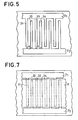
- the grid G 1 has fingers 31, 33, etc., perpendicular to the section plane of FIG. 4.
- the grid G 2 has fingers 32, 34 etc ... parallel to the fingers 31, 33.
- the distance “d between the fingers 31 and 32 (or between 33 and 34) is fixed at a predetermined value according to the diagram of the Figure 1, while the distance between the fingers 32 and 33 or the like may be different.
- FIGs 6 and 7 there is shown respectively in section and in top view, the result of a step in which a layer 6 of gallium arsenide has been grown by epitaxy so as to drown the fingers of the two grids G 1 and G 2 .
- Layer 6 is limited in width so that we have access to the grid bars to connect them to the bias voltage generators.
- the gallium arsenide of layer 6 is doped in an identical manner to that of layer 5: in this way a single layer 7 is thus produced. in which the fingers of the two grids G 1 and G 2 are embedded.
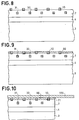
- FIG. 8 there is shown in section the result of a step in which source contacts 10 have been deposited in the form of fingers parallel to the gate fingers 31 and 32, but taking care to place each contact 10 at equal distance from each of the fingers 31 and 32.
- Layer 7 is 0.2 to 0.3 micron thick.
- FIG. 9 the result of a step has been shown in which an insulator 90 has been deposited between the source contacts 10.
- the upper part of the contacts 10 has been previously protected by selectively depositing at the using photolithographic methods of the resin pins on the contacts 10. This intermediate step is not shown.
- a deposition of silica was carried out (SIOJ on the whole of the device and the resin pins and the silica which covered them were eliminated, causing a solvent to act on the resin.
- FIG. 10 shows the result of a step in which a metal plate 100, relatively much thicker than the semiconductor layers 4 and 7, of which the scale is specially enlarged, has been deposited.
- the plate 100 is intended to allow access, in parallel, to the source contacts 10. It projects beyond the semiconductor block along an edge 71 of the latter.
- the next two steps consist in eliminating the semiconductor substrate and replacing it with an insulating support on the side of the plate 100.
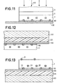
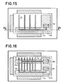
- the following steps consist in establishing several rows of anode or target contacts with fingers parallel to the fingers of the grids G 1 and G 2 (Schottky contacts 31 and 32).
- the pitch of the row of fingers of each target remains equal to the distance separating two consecutive source contacts, ie 1 micron in the above example, the difference between the targets being less than one micron.
- the method of manufacturing a phase-shifting device according to the invention comprises steps identical to those which have just been described, with the exception of the last steps concerning the deposition of the anode contacts. These steps are replaced by a single step during which carries out a metallic deposition on the layer 7 (FIG. 12) to constitute the target electrode 20, as shown in FIG. 2.
Landscapes
- Junction Field-Effect Transistors (AREA)
- Bipolar Transistors (AREA)
- Electrodes Of Semiconductors (AREA)
Claims (11)
Applications Claiming Priority (2)
| Application Number | Priority Date | Filing Date | Title |
|---|---|---|---|
| FR8101466 | 1981-01-27 | ||
| FR8101466A FR2498815A1 (fr) | 1981-01-27 | 1981-01-27 | Dispositif semi-conducteur de deviation d'electrons du type " a transport balistique ", et procede de fabrication d'un tel dispositif |
Publications (2)
| Publication Number | Publication Date |
|---|---|
| EP0058577A1 EP0058577A1 (de) | 1982-08-25 |
| EP0058577B1 true EP0058577B1 (de) | 1984-06-13 |
Family
ID=9254548
Family Applications (1)
| Application Number | Title | Priority Date | Filing Date |
|---|---|---|---|
| EP82400033A Expired EP0058577B1 (de) | 1981-01-27 | 1982-01-08 | Halbleiteranordnung mit Elektronenablenkung vom Typ des "ballistischen Transportes" und Verfahren zum Herstellen einer solchen Anordnung |
Country Status (6)
| Country | Link |
|---|---|
| US (1) | US4563696A (de) |
| EP (1) | EP0058577B1 (de) |
| JP (1) | JPS57143870A (de) |
| CA (1) | CA1177583A (de) |
| DE (1) | DE3260213D1 (de) |
| FR (1) | FR2498815A1 (de) |
Families Citing this family (7)
| Publication number | Priority date | Publication date | Assignee | Title |
|---|---|---|---|---|
| US5298787A (en) * | 1979-08-10 | 1994-03-29 | Massachusetts Institute Of Technology | Semiconductor embedded layer technology including permeable base transistor |
| US4712122A (en) * | 1984-07-26 | 1987-12-08 | Research Development Corp. | Heterojunction gate ballistic JFET with channel thinner than Debye length |
| DE3432901C1 (de) * | 1984-09-07 | 1986-01-16 | Licentia Patent-Verwaltungs-Gmbh, 6000 Frankfurt | Halbleiteranordnung |
| US4866660A (en) * | 1988-02-29 | 1989-09-12 | Amp Incorporated | Optoelectraulic devices based on interference induced carrier modulation |
| EP0416198A1 (de) * | 1989-08-30 | 1991-03-13 | International Business Machines Corporation | Elektronenwellenablenkung in modulationsdotierten und anderen dotierten Halbleiterstrukturen |
| JPH05315598A (ja) * | 1992-05-08 | 1993-11-26 | Fujitsu Ltd | 半導体装置 |
| US7440227B2 (en) * | 2005-02-28 | 2008-10-21 | Hitachi Global Storage Technologies Netherlands B.V. | Magnetic head having a hall effect sensor and circuit for detecting recorded bits from magnetic recording media |
Family Cites Families (5)
| Publication number | Priority date | Publication date | Assignee | Title |
|---|---|---|---|---|
| US3560963A (en) * | 1968-06-27 | 1971-02-02 | Theodore R Trilling | Field effect a/d converter |
| US3593045A (en) * | 1969-12-29 | 1971-07-13 | Bell Telephone Labor Inc | Multiaddress switch using a confined electron beam in a semiconductor |
| US4129880A (en) * | 1977-07-01 | 1978-12-12 | International Business Machines Incorporated | Channel depletion boundary modulation magnetic field sensor |
| DE2804165C2 (de) * | 1978-02-01 | 1982-11-11 | Licentia Patent-Verwaltungs-Gmbh, 6000 Frankfurt | Halbleiteranordnung mit einem für die Stromführung geeigneten Kanal und Verfahren zum Betrieb dieser Halbleiteranordnung |
| US4366493A (en) * | 1980-06-20 | 1982-12-28 | International Business Machines Corporation | Semiconductor ballistic transport device |
-
1981
- 1981-01-27 FR FR8101466A patent/FR2498815A1/fr active Granted
-
1982
- 1982-01-08 DE DE8282400033T patent/DE3260213D1/de not_active Expired
- 1982-01-08 EP EP82400033A patent/EP0058577B1/de not_active Expired
- 1982-01-20 US US06/340,965 patent/US4563696A/en not_active Expired - Fee Related
- 1982-01-25 CA CA000394852A patent/CA1177583A/en not_active Expired
- 1982-01-26 JP JP57009620A patent/JPS57143870A/ja active Granted
Also Published As
| Publication number | Publication date |
|---|---|
| US4563696A (en) | 1986-01-07 |
| FR2498815B1 (de) | 1983-02-18 |
| JPH0261146B2 (de) | 1990-12-19 |
| CA1177583A (en) | 1984-11-06 |
| DE3260213D1 (en) | 1984-07-19 |
| EP0058577A1 (de) | 1982-08-25 |
| JPS57143870A (en) | 1982-09-06 |
| FR2498815A1 (fr) | 1982-07-30 |
Similar Documents
| Publication | Publication Date | Title |
|---|---|---|
| EP0350351B1 (de) | Fotodiode und Fotodiodenmatrix aus II-VI-Halbleitermaterial und Herstellungsverfahren dafür | |
| EP0267824B1 (de) | Transistor-gesteuerter elektrooptischer Anzeigeschirm und Verfahren zu seiner Herstellung | |
| EP0258141B1 (de) | MIS integrierte Schaltung, wie eine EPROM-Speicherzelle, und Verfahren zu deren Herstellung | |
| EP0222668B1 (de) | Verfahren zum Herstellen eines Dünnschichttransistors mit in Bezug auf Source und Drain selbstausrichtendem Gate durch stufenweises Ätzen und danach hergestellter Transistor | |
| FR2663158A1 (fr) | Procede de fabrication de transistor a effet de champ. | |
| EP0223780B1 (de) | Verfahren zum herstellen von mos-transistoren mit metallsilicidelektroden | |
| FR3060838A1 (fr) | Procede de realisation d'un dispositif semi-conducteur a canal contraint en compression | |
| EP0617839B1 (de) | Verfahren zur Herstellung von Halbleiterkomponenten, insbesondere auf GaAs oder InP, bei dem das Substrat auf chemischem Wege wiedergewonnen wird | |
| EP0140772A2 (de) | PIN-Dioden als Leistungsbegrenzer für Millimeterwellen und Verfahren zum Herstellen der Dioden | |
| FR2662854A1 (fr) | Structure de trou de connexion isolee pour des dispositifs a semiconducteurs et procede de fabrication. | |
| FR2510819A1 (fr) | Procede de fabrication d'un composant misfet et composant misfet ainsi produit | |
| EP0461967A2 (de) | Halbleiteranordnung mit Schottky-Übergang für Mikrowellenverstärkung und schnelle logische Schaltungen und Verfahren zu deren Herstellung | |
| EP0214033B1 (de) | Verfahren zur Herstellung eines Lichtbildsensors und linearer Bildsensor durch dieses Verfahren | |
| EP0166647A1 (de) | Verfahren zum Herstellen von wenigstens einem Dünnschichtfeldeffekttransistor und nach diesem Verfahren hergestellter Transistor | |
| EP0058577A1 (de) | Halbleiteranordnung mit Elektronenablenkung vom Typ des "ballistischen Transportes" und Verfahren zum Herstellen einer solchen Anordnung | |
| FR2464564A1 (fr) | Batterie solaire au silicium amorphe | |
| EP1483793A2 (de) | Leistungs-schottkydiode mit sicoi-substrat und diesbezügliches herstellungsverfahren | |
| EP0448465B1 (de) | Optisches Detektionsverfahren mit verstellbarer Detektionsschwelle | |
| EP1218942A1 (de) | Halbleiterbauelement mit den vorteilen von den soi und massiv aufbau und verfahren zur deren herstellung | |
| EP0310184A1 (de) | Optisches Schaltelement aus zwei parallelen Lichtleitern und aus solchen Elementen zusammengesetzte Schaltmatrix | |
| EP1507286A2 (de) | Herstellungsverfahren unter einer dünnen Schicht eines ersten Materials von Teilen eines anderen Materials und/oder von Luftspalten | |
| EP4033540A1 (de) | Vorrichtung mit elektrostatischen steuergates, die auf zwei gegenüberliegenden seiten eines halbleiterabschnitts verteilt sind | |
| FR2659495A1 (fr) | Connecteur elastomerique pour circuits integres ou analogues, et son procede de fabrication. | |
| EP0263755B1 (de) | Verfahren zur Herstellung einer P+NN+-Diode und eines diese Diode umfassenden bipolaren Transistors unter Verwendung des Neutralisierungseffektes von atomarem Wasserstoff auf Donatoratomen | |
| FR2525814A1 (fr) | Procede de formation d'une couche protectrice dans une structure a semi-conducteurs |
Legal Events
| Date | Code | Title | Description |
|---|---|---|---|
| PUAI | Public reference made under article 153(3) epc to a published international application that has entered the european phase |
Free format text: ORIGINAL CODE: 0009012 |
|
| AK | Designated contracting states |
Designated state(s): DE GB IT NL |
|
| 17P | Request for examination filed |
Effective date: 19821008 |
|
| ITF | It: translation for a ep patent filed | ||
| GRAA | (expected) grant |
Free format text: ORIGINAL CODE: 0009210 |
|
| AK | Designated contracting states |
Designated state(s): DE GB IT NL |
|
| REF | Corresponds to: |
Ref document number: 3260213 Country of ref document: DE Date of ref document: 19840719 |
|
| PLBE | No opposition filed within time limit |
Free format text: ORIGINAL CODE: 0009261 |
|
| STAA | Information on the status of an ep patent application or granted ep patent |
Free format text: STATUS: NO OPPOSITION FILED WITHIN TIME LIMIT |
|
| 26N | No opposition filed | ||
| PGFP | Annual fee paid to national office [announced via postgrant information from national office to epo] |
Ref country code: DE Payment date: 19881230 Year of fee payment: 8 |
|
| PGFP | Annual fee paid to national office [announced via postgrant information from national office to epo] |
Ref country code: GB Payment date: 19890108 Year of fee payment: 8 |
|
| ITTA | It: last paid annual fee | ||
| PGFP | Annual fee paid to national office [announced via postgrant information from national office to epo] |
Ref country code: NL Payment date: 19890131 Year of fee payment: 9 |
|
| PG25 | Lapsed in a contracting state [announced via postgrant information from national office to epo] |
Ref country code: GB Effective date: 19900108 |
|
| PG25 | Lapsed in a contracting state [announced via postgrant information from national office to epo] |
Ref country code: NL Effective date: 19900801 |
|
| GBPC | Gb: european patent ceased through non-payment of renewal fee | ||
| NLV4 | Nl: lapsed or anulled due to non-payment of the annual fee | ||
| PG25 | Lapsed in a contracting state [announced via postgrant information from national office to epo] |
Ref country code: DE Effective date: 19901002 |