EP0063483B1 - Circuit semi-conducteur intégré - Google Patents
Circuit semi-conducteur intégré Download PDFInfo
- Publication number
- EP0063483B1 EP0063483B1 EP82301967A EP82301967A EP0063483B1 EP 0063483 B1 EP0063483 B1 EP 0063483B1 EP 82301967 A EP82301967 A EP 82301967A EP 82301967 A EP82301967 A EP 82301967A EP 0063483 B1 EP0063483 B1 EP 0063483B1
- Authority
- EP
- European Patent Office
- Prior art keywords
- voltage
- semiconductor integrated
- circuit
- integrated circuit
- power source
- Prior art date
- Legal status (The legal status is an assumption and is not a legal conclusion. Google has not performed a legal analysis and makes no representation as to the accuracy of the status listed.)
- Expired
Links
Images




Classifications
-
- H—ELECTRICITY
- H10—SEMICONDUCTOR DEVICES; ELECTRIC SOLID-STATE DEVICES NOT OTHERWISE PROVIDED FOR
- H10D—INORGANIC ELECTRIC SEMICONDUCTOR DEVICES
- H10D89/00—Aspects of integrated devices not covered by groups H10D84/00 - H10D88/00
- H10D89/211—Design considerations for internal polarisation
- H10D89/213—Design considerations for internal polarisation in field-effect devices
-
- G—PHYSICS
- G05—CONTROLLING; REGULATING
- G05F—SYSTEMS FOR REGULATING ELECTRIC OR MAGNETIC VARIABLES
- G05F1/00—Automatic systems in which deviations of an electric quantity from one or more predetermined values are detected at the output of the system and fed back to a device within the system to restore the detected quantity to its predetermined value or values, i.e. retroactive systems
- G05F1/10—Regulating voltage or current
- G05F1/46—Regulating voltage or current wherein the variable actually regulated by the final control device is DC
- G05F1/462—Regulating voltage or current wherein the variable actually regulated by the final control device is DC as a function of the requirements of the load, e.g. delay, temperature, specific voltage/current characteristic
- G05F1/465—Internal voltage generators for integrated circuits, e.g. step down generators
-
- G—PHYSICS
- G11—INFORMATION STORAGE
- G11C—STATIC STORES
- G11C11/00—Digital stores characterised by the use of particular electric or magnetic storage elements; Storage elements therefor
- G11C11/21—Digital stores characterised by the use of particular electric or magnetic storage elements; Storage elements therefor using electric elements
- G11C11/34—Digital stores characterised by the use of particular electric or magnetic storage elements; Storage elements therefor using electric elements using semiconductor devices
- G11C11/40—Digital stores characterised by the use of particular electric or magnetic storage elements; Storage elements therefor using electric elements using semiconductor devices using transistors
- G11C11/401—Digital stores characterised by the use of particular electric or magnetic storage elements; Storage elements therefor using electric elements using semiconductor devices using transistors forming cells needing refreshing or charge regeneration, i.e. dynamic cells
- G11C11/4063—Auxiliary circuits, e.g. for addressing, decoding, driving, writing, sensing or timing
- G11C11/407—Auxiliary circuits, e.g. for addressing, decoding, driving, writing, sensing or timing for memory cells of the field-effect type
- G11C11/4074—Power supply or voltage generation circuits, e.g. bias voltage generators, substrate voltage generators, back-up power, power control circuits
-
- G—PHYSICS
- G11—INFORMATION STORAGE
- G11C—STATIC STORES
- G11C5/00—Details of stores covered by group G11C11/00
- G11C5/14—Power supply arrangements, e.g. power down, chip selection or deselection, layout of wirings or power grids, or multiple supply levels
- G11C5/145—Applications of charge pumps; Boosted voltage circuits; Clamp circuits therefor
-
- G—PHYSICS
- G11—INFORMATION STORAGE
- G11C—STATIC STORES
- G11C5/00—Details of stores covered by group G11C11/00
- G11C5/14—Power supply arrangements, e.g. power down, chip selection or deselection, layout of wirings or power grids, or multiple supply levels
- G11C5/147—Voltage reference generators, voltage or current regulators; Internally lowered supply levels; Compensation for voltage drops
Definitions
- the present invention relates to a highly dense integrated circuit and, more particularly, to an integrated circuit which is suitable for a highly dense semiconductor memory.
- JP-A-51-104276 a technique, in which two kinds of gate oxide film thicknesses and two kinds of gate region surface concentrations are combined for high integration of a semiconductor memory.
- JP-A-50-119543 moreover, there is disclosed a concept, in which the channel length or diffusion layer spacing of the transistors of a memory array unit is further reduced by implanting ions of high concentration in the Si surface of the memory array unit thereby to increase the integration.
- the size of circuit elements such as transistors is reduced by those techniques, the withstand voltage of those circuit elements against dielectric breakdown has to be reduced. Therefore, it is necessary to reduce either the power source voltage fed to those circuit elements or the signal voltage generated by those circuit elements in accordance with the reduction in the size of the circuit elements.
- the voltage impressed from the outside i.e., the voltage impressed upon the power source pin of the package of a memory LSI
- the conventional techniques thus far described have failed to realize a highly integrated memory which can use a high external voltage. This fact is not limited to memory devices but also applies to other integrated circuits.
- a semiconductor integrated circuit comprising: a first circuit (30) arranged to receive a first power source voltage (V cc ) and to generate a predetermined second power source voltage (V DP ) which is lower than said first power source voltage; a second circuit (50, 50A, PG) arranged to receive said first power source voltage (V cc) and/ or the second power source voltage and to generate a second pulse signal for use with said second power source voltage, in response to a first pulse signal which varies within a voltage range of said first power source voltage and/or the second power source voltage; and a third circuit (40) arranged to receive said second power source voltage and responsive to said second pulse signal, said third circuit including circuit elements (Q m ) having a smaller size than that of the circuit elements forming said first circuit.
- those circuit elements in the second circuit which are made responsive to a signal having a larger amplitude, are made to have a larger size so that they may have a high withstand voltage
- those circuit elements of the third circuit which are made responsive to the output signal of the second circuit, are made to have a smaller size so that they may be highly integrated.
- the first circuit is suitably constructed of circuit elements having a large size and is arranged to receive the high first power source voltage for feeding the second power source voltage, which is lower than the first power source voltage, to the third circuit.
- the second circuit is made operative to feed the third circuit with a signal which has a voltage corresponding to the second power source voltage.
- the first and second circuit can be fabricated without any problem concerning the withstand voltage whereas the third circuit is constructed of circuit elements having a smaller size and occupies a larger area in the integrated circuit as a whole, high integration can be achieved when the integrated circuit is considered as a whole.
- the channel length L and the threshold voltage V th can be reduced as a result that the thin oxide film can be selectively used, as is apparent from the general characteristics of the MOST.
- high integration can be effected without any reduction in the speed by positively adopting the possibility of the reduction.
- the region of the thin oxide film can inevitably have its L and V th reduced although it has a low operating voltage so that it has to perform nothing but a low-speed operation.
- the positive reduction of the L and V th will lead to the desired high-speed operation.
- Element separation can be facilitated at a region which is operated at a low voltage.
- the element separation width can be accordingly reduced.
- the desired high integration can be effected.
- the inter-layer film thickness which contributes to the element separation characteristics can be reduced.
- a flatter device can be produced, reducing the tendency of the wiring layer (which may be Al, for example) to break, and producing a high yield.
- the depth x j of the diffusion layer of the major portion of both a memory array and a direct peripheral circuit is made smaller than that of an indirect peripheral circuit unit. This is because a MOST having the smaller size can be used for the smaller x j .
- Fig. 1 is a sectional view of such a memory chip for a dynamic memory as is composed of a P-type substrate 10, and illustrates the concept of the present system.
- An N-type MOS transistor (which will be abbreviated as "MOST") Qp has a thicker gate oxide film t ox2 than the gate oxide film t ox1 of an MOST Q m and has a drain Dp fed with a higher drain voltage, e.g., an external voltage V cc (e.g., 5 V).
- MOST N-type MOS transistor
- the drain D m of the MOST Q m is fed with a lower voltage V DP (e.g., 3.5 V) than the voltage V cc by the action of an internal power source voltage generating circuit 30 (which is actually formed in the substrate 10) which in turn is fed with that voltage V cc .
- V DP e.g., 3.5 V
- This external voltage V cc is fed to a substrate voltage generating circuit 20, by which the bias voltage of the substrate 10, e.g., -3 V is generated.
- that circuit 20 is shown outside of the substrate 10 but is disposed in fact in the substrate 10.
- the integration of a memory is determined by the integrations of the memory array and a first circuit unit 40 composed of a peripheral circuit (i.e., a direct peripheral circuit), which is directly connected with the memory array, such as a sense amplifier (although not shown) for either driving that memory array or amplifying a minute signal generated by the memory array. It is, therefore, desired to reduce the size of the MOST Q m of that portion.
- This size can be generally reduced from the relationship of the withstand voltage, the hot electrons and the substrate current of the MOST Q m by dropping the operating voltage.
- the reduction in the size of the MOST O m is realized by thinning the gate oxide film t ox1 of the MOST Q m , by dropping the drain voltage to the voltage V DP lower than the external voltage V cc and by reducing the channel length.
- a second circuit unit 50 which is composed of another control circuit, i.e., a circuit (i.e., an indirect peripheral circuit) for controlling the direct peripheral circuit occupies about 10% of the whole area of the chip thereby to make it unnecessary to use an MOST having an especially small area. Rather, since that indirect peripheral circuit is connected with an external input terminal, its withstand voltage against dielectric breakdown has to be sufficiently high. For this requirement, it is generally necessary to thicken the gate oxide film t ox2 of the MOST Qp and to accordingly enlarge the size (e.g., the channel length) of the MOST Qp used.
- the drain voltage of the MOST Qp is set at the voltage V cc higher than the drain voltage V DP of the MOST Q m . It is quite natural that the minimum of the voltage of the gate Gp is generally set at the external voltage V cc . Incidentally, the sources Sp and S m of the MOSTs Q P and Q m are both maintained at the earth potential. As shown in Fig.
- the size of the MOST Q m of the first circuit 40, which is constructed of the memory array and the direct peripheral circuit both influencing the high integration, is reduced, whereas the size of the MOST Qp of the second circuit unit 50 constructed of the indirect peripheral circuit is enlarged.
- the MOST Qp is enabled to operate by using the power source voltage (V cc . e.g., at 5 V) from the outside of the chip as the operating voltage.
- the MOST Q m is enabled to operate at a lower operating voltage V D p, e.g., 3.5 V) by converting the power source voltage V cc in the chip.
- the threshold voltage V th is dropped in accordance with the lower operating voltage. Since, in this respect, the threshold voltage V th is dropped in accordance with the general characteristics of an MOST as a gate oxide film t ox is made smaller, the operating speed of the first circuit unit occupying the major portion of the operating speed of the memory can be accelerated.
- the present system is advantageous in having a high speed.
- the threshold voltage V th can be properly adjusted by the ion implanting technique in accordance with the application.
- the present system can be effectively used by taking several points into consideration when it is applied to the actual dynamic N-type MOS memory which is constructed of a one-transistor type memory cell.
- One example is shown in Fig. 2 and is directed to a memory having folded type data lines.
- This memory is constructed to include: the substrate bias generating circuit 20 which receives the external power source voltage V cc (at 5 V) for generating a substrate bias voltage of about -3 V; the internal power source generating circuit 30 which receives the external power source voltage V cc for generating the internal power source voltage of 3.5 V and a d.c.
- the indirect peripheral circuit 50 which receives to the external power source voltage V cc , external addresses Ai to Aj and Ai' to Aj' and an external control signal for generating internal address signals a to a j and a,' to a j ' and internal control pulses ⁇ 0 , ⁇ 1 , ⁇ 3 , ⁇ x and ⁇ y ; and a memory array MA and the direct peripheral circuit 40 adapted to be controlled by the voltages V DP and V' and address signals a, to a j and a 1 ' to a j ' and the control pulses ⁇ 0' ⁇ 1 and ⁇ 3 .
- That direct peripheral circuit is composed of an X decoder XD, a Y decoder YD, a pre-charge circuit PC and a sense amplifier SA.
- a circuit 50A corresponds to that portion of the indirect peripheral circuit 50, which is made operative to generate word line drive pulses and is shown separately from the circuit 50.
- the pulses ⁇ 1 ' and ⁇ x ' shown in that circuit 50A are generated in the indirect peripheral circuit 50.
- both the external address signals and the external control signals to be fed to the indirect peripheral circuit 50 are signals which vary between the external power source voltage V cc and the earth potential.
- the pulses ⁇ 1 ' a to a j and a l ' to a j ' are all pulses which vary between the internal power source voltage VDp and the earth potential;
- the pulses ⁇ 0 are pulses which take a higher level than the sum of the voltage V D p and V th if this latter voltage V th is designated to mean the threshold value of the pre-charge transistors Qp, Qp, Q DP , O YO and Q xo ;
- the pulses ⁇ 3 are pulses which take such a level as is lower than the voltage V D p by the threshold value of transistors Q A and Q A .
- the pulses ⁇ x and ⁇ y are pulses which take the level of the voltage V DP .
- the read-out signal voltages which are fed from a selected memory cell MC of the memory array MA to appear on a data line D in accordance with stored data, are judged to be data "1" and "0" by the sense amplifier SA with reference to a reference voltage which is fed from a dummy cell DC to appear on a data line D, and this process will be described in the following. Specifically, after the respective paired data lines D and D have been precharged to the voltage V DP (lower than the voltage V cc ) by the pre-charge signals ⁇ 0 , these signals ⁇ 0 disappear so that the lines D and D are maintained at the voltage V DP .
- the amplitude of those precharge signals ⁇ 0 may be sufficiently higher than the voltage Vop (i.e., than the sum of the voltages V DP ) so that the precharge levels of the lines D and D may be prevented from being unbalanced (which produces equivalent noises during the reading operation) by the influences of the fluctuations of the threshold value of the MOSTs Qp and Qp in the data line pre- charge circuit PC.
- the word start pulses ⁇ x ' which has an amplitude of the external power source voltage V cc
- WG word voltage generating circuit
- a word driver MOST Q xs Since the decoder XD has already been selected by that time by the addresses a, to a j , a word driver MOST Q xs has its gate maintained at the high level. In other words, the MOST Q xs is rendered conducting.
- the word voltage generating circuit WG is made responsive to the pulses ⁇ x ' to generate the pulses ⁇ x having an amplitude V D p and has its output ⁇ x transmitted as it is from a node W' to the word line W.
- a booster circuit VU receives the pulses ⁇ 1 ' (which have an amplitude V cc ) to generate the pulses ⁇ 1 . These pulses ⁇ 1 are impressed upon the node W' through the boost trap capacitor C B .
- the word line has its voltage boosted.
- the boost voltage in this case is so determined by the parasitic capacitance, which is the sum of the capacitor C B , the node W' and the line W, and by the amplitude of the pulses ⁇ 1 that it can take a value as high as 0.5 V D p.
- pulses having an amplitude of about 1.5 V DP are generated on the line W.
- a pulse voltage of 1.5 V DP is generated on the dummy word line DW by a circuit of a similar kind.
- the amplification is conducted by dropping the voltage of the pulses ⁇ 3 , which have been precharged during the pre-charge by the data lines D and D to the level of V DP ⁇ V th (which is the voltage V th of the MOSTs Q A and A A ), to 0 V.
- the differential signals of the lines D and D thus amplified are fed to I/O and I/O , which are shared between the respective paired data lines, by selecting the predetermined Y decoder YD by the addresses a i ' to a j ' (so that the gate voltage of a MOST Qy s is raised to the high level) and by impressing the pulses ⁇ y which have been boosted to 1.5 V DP until they become the data output.
- the withstand voltage naturally raises a problem if the integration is increased, that is to say, the memory cell is reduced, as has been described hereinbefore, while maintaining the voltage V cc at 5 V.
- the operating voltages of the memory cell MC and the dummy cell DC which have direct relationship with the integration, and the direct peripheral circuit and MOSTs (e.g.
- the elements in the direct peripheral circuit can be used by having their sizes selectively enlarged, as the case may be, if the operating state is taken into consideration.
- the MOST Q CL is fed with the high voltage of 1.5 V D p between its drain and source thereby to make it necessary to devise the user of an MOST having a larger size.
- the MOSTs Q A and Q A may fail to have their threshold values coincide as a result of dispersion in their production if their sizes are reduced so much. Since such lack of coincidence invites read-out noises in the memory cell, it is necessary to selectively enlarge the sizes of the MOSTs Q A and Q A .
- Fig. 3 the specific sizes of the elements in the memory of Fig. 2 are exemplified in Fig. 3.
- the combinations of those various sizes can be selected in accordance with the application. For example, if two different combinations of the depth x j of a diffusion layer and the thickness top of an insulating film are used as in Fig. 3, the advantage of the present invention can be enjoyed to the maximum. However, only one such combination may be used in order to facilitate production.
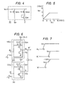
- Fig. 4 is a circuit diagram showing the internal power source voltage generating circuit 30.
- N-channel MOSTs Q DN 1 and Q DN 2 of depletion type have their drains fed with the external power source voltage V cc . Since the threshold voltage V th of those MOSTs is selected to be -3.5 V, the source potential of the MOST Q DN 1 is maintained at 3.5 V. From this source terminal, there can be generated the internal power source voltage V DP which is impressed upon the respective portions of the memory chip.
- the source of the MOST Q DN 2 is connected with the drain and gate of an enhancement type MOST Q EH having a threshold voltage of 0.5 V so that a power source voltage V' of 3.0 V is generated from the source terminal of the latter transistors.
- Fig. 5 illustrates the relationship between the external and internal power source voltages V cc and VDp of the embodiment under consideration.
- Fig. 6 shows the circuit constructions of the word voltage generating circuit WG and the voltage boosting circuit VU of Fig. 2.
- the operations of these circuits WG and VU are illustrated in wave forms in Fig. 7.
- Each of the circuits WG and VU is constructed to include: a voltage converter 130a or 130b, which is composed of the depletion type N-channel and a conventional pulse generating circuit PG.
- the amplitude of the input pulse voltages ⁇ x ' and ⁇ 1 ' is V cc
- the voltage at a point a is maintained at 3.5 V by the action of the depletion MOST Q oN .
- the pulse generating circuit PG in the voltage boosting circuit VU generates the pulses ⁇ 1 of the voltage V D p in response to the rise of the input pulses ⁇ 1 ' (which have the amplitude V co ).
- the node W' has its voltage boosted to about 1.5 V D p by the action of the capacitance C B .
- the output voltage of the circuit PG is substantially constant even with the change in the voltage V cc (e.g., from 5 to 8 V), because it is exclusively determined by the threshold voltage V th of an MOST Q DN (as shown in Fig. 5). This means that the minute MOSTs used in multiplicity in the memory array MA and the direct peripheral circuit can be protected from any breakage even if the voltage V cc is made excessively high.
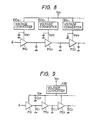
- Fig. 8 schematically shows the internal construction of the indirect peripheral circuit.
- Pulse generating circuits PG1, PG2 and PG3, which are connected in tandem for generating timing signals, are respectively equipped with voltage converters 130a, 130b and 130c which are similar to those shown in Fig. 6, and are respectively fed with a voltage which is equal to the internal power source voltage V DP .
- Fig. 9 is a circuit diagram shown in comparison with Fig. 8.
- the pulse generating circuits are equipped with a common voltage converter 130.
- the plural circuits PG interfere with one another in the form of the fluctuations in the voltage VDp so that ideal pulse waveforms cannot be generated by the respective circuits PG. This defect is solved by the construction of Fig. 8.
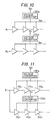
- Fig. 10 shows another embodiment for reducing that mutual interference through the voltage Vop which has the defect concomitant with the construction of Fig. 8.
- the circuits PG constructing the indirect peripheral circuit are classified into plural groups of the circuits PG in accordance with the operating time band such that some circuits PG operated only during a certain time band whereas the remaining plural circuits PG operate during a different time band.
- the dynamic memory of address multiplex type for example, there exist in the chip two groups of the circuits PG which are made operative to correspond to the two externally impressed clocks ( ⁇ 1 and w2), respectively.
- circuits PG into the circuits PG (e.g., PG1, PG2, PG3 and so on), which are made operative in the case of existence of the input signals ⁇ , and the circuits PG (e.g., PG1', PG2', PG3' and so on), which are made operative in the case of non-existence, that is to say, into two groups of the circuits PG, which are made operative in a manner to correspond to the logic states of the signals ⁇ , and to connect those two groups with the voltage converters 130a and 130b, respectively.
- the circuits PG e.g., PG1, PG2, PG3 and so on
- the circuits PG e.g., PG1', PG2', PG3' and so on
- the MOST Q L is rendered conducting so that the output ⁇ 0 is changed from the low potential (i.e., 0 V) to the high potential (i.e., V cc ) '
- the generation of the output pulses at the low voltage by the use of the circuit of that type can be effected by the example shown in Fig. 6. As the case may, however, if the pulses ⁇ 1 having an amplitude equal to that of the externally fed power source voltage V cc shown in Fig. 13 are supplied, the amplitude of the outputs ⁇ 01 to ⁇ 04 of the respective circuits PG is also V cc .
- pulses e.g., ⁇ 01 ' and ⁇ 04 '
- VDp voltage amplitude
- Examples of the voltage converter 130 in this case are shown in Figs. 14 and 15.
- Fig. 14 shows an example, in which inverters Q,' and Q D ' for the pulses ⁇ 0 ' are added in parallel to the output step of the circuit of Fig. 12.
- a MOST Q DN is the same depletion type MOST as that of Fig. 6.
- Fig. 15 shows an example, in which the same depletion type MOST Q DN as that of Fig. 6 is added in series with the MOSTs Q D and Q L so that the output is fed out of both the two terminals thereof.
- the pulses ⁇ 0 can have an amplitude up to the voltage V cc , and the pulses ⁇ 0 ' (which are regulated by the threshold voltage of the depletion MOST so that it acquires the amplitude V DP ) are generated at the same time as the pulses ⁇ 0 .
- Fig. 16 shows an example, in which the pulses ⁇ 0 ' of Fig. 15 are boosted, as shown in Fig. 6.
- a constant voltage circuit is used as the internal power source voltage generating circuit 30, and the voltage converter 130 used, which is connected with the respective pulse generating circuits included in the indirect peripheral circuit 50. is correspondingly of constant voltage characteristics.
- an aging test in which a higher voltage than the voltage used in the usual operation is intentionally impressed upon the respective transistors in the circuit thereby to discover at an initial stage any transistor which is liable to be troubled by intrinsic degradation in the gate oxide film, thus ensuring reliability.
- a sufficient aging voltage is not applied to the aforementioned circuit portion of the low withstand voltage, in the integrated circuit chip which is so constructed as to feed the power source voltage to the circuit portion through the constant voltage circuit in the chip.
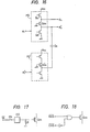
- Figs. 17 and 18 show means for eliminating the aforementioned defect.
- the gate voltage of the voltage limiting depletion MOST Q DN which is included in either the internal power source voltage generating circuit 30 shown in Fig. 5 or the voltage converter of Fig. 6 or the like, is set at the earth potential during the usual operation and at a suitable voltage V E during the aging operation.
- the gate of the MOST Q DN is grounded to the earth in the chip through a resistance R in the chip.
- the gate is connected through a bonding pad PD with the pin PN of the package. If that pin is left open during the usual operation, the gate of each MOST Q DN is at the earth potential. If that pin is fed with a voltage during the aging operation, on the other hand, a voltage, which is raised by the application of that voltage, is generated at the source of the MOST Q DN .
- Fig. 18 shows an embodiment, in which the phase relationship of the external clocks to be applied to the chip is adjusted only during the aging operation without any elaborate provision of an aging pin, as in the foregoing description, so that the same effect may be attained.
- a dynamic RAM is operated by a suitable relationship between two kinds of external clocks RAS (i.e., Row Address Strobe) and CAS (Column Address Strobe). Since the combination of the RAS at the high level and the CAS at the low level is not usually used, conversely the combination may be used during the aging operation.
- RAS Row Address Strobe
- CAS Cold Address Strobe
- the voltage VDp limited to a predetermined value has been used as the internal power source voltage, such as internal power source voltage V cc2 as can be varied with the variation in the external power source voltage V cc is used in the embodiment to be described while considering the effect of the aforementioned aging test.
- Fig. 19 shows the basic circuit of the internal power source voltage generating circuit which is used in place of the circuit of Fig. 4 so as to generate such an internal power source voltage V cc2 as can be varied.
- Voltage dividing means 32 which is composed of resistors R, and R 2 , has its middle point connected with the gate of an enhancement type MOST Q LL whereas one terminal of the resistor R, and the drain of the transistor Q LL are fed with the external power source voltage V cc .
- the internal power source voltage V cc2 to be obtained for the output voltage V LL of the voltage dividing means 32 can be expressed by the following Equation: wherein V th designates the threshold voltage of the MOST Q LL .
- Fig. 20 is a graph showing the variation in the internal power source voltage V cc2 , which is generated by the circuit of Fig. 19, with reference to the variation in the external power source voltage V cc .
- FIG. 20 shows the example in which the internal power source voltage V cc2 is varied with an identical constant of proportion all over the range, it is possible to generate an internal power source voltage V cc2 having various characteristics if the voltage dividing means 32 of Fig. 19 is modified.
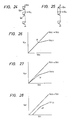
- Fig. 21 shows voltage dividing. means, which is composed of a number n of diodes D connected in series and the resistor R 1 . If this voltage dividing means is used as the internal power source voltage generating means, the internal power source voltage V cc2 is expressed in Fig. 26.
- V cc2 (p) at a point P is a voltage at the instant when the n diodes D are turned on and can be substantially expressed by the following Equation: wherein V F designates the forward voltage of each diode D.
- the gradient after the point P is determined by the resistance of the resistor R 1 and by the equivalent ON resistance n - R D of the diodes D.
- Fig. 22 shows an example in which the aforementioned diodes D are replaced by an MOST Q c .
- the voltage V CC2 (p) at this time is expressed by the following Equation: wherein V th designates the threshold voltage of the MOST Q c .
- the gradient after the point P is determined similarly to the above by the resistor R 1 and by the equivalent ON resistance n . Roc.
- Fig. 23 shows voltage dividing means which is constructed by adding a resistor R 3 in parallel to the series MOSTs Q c of the voltage dividing means of Fig. 22. If the means of Fig. 23 is used, the internal power source voltage V cc2 of Fig. 27 can be generated.
- Fig. 24 shows an example, in which the resistor R 1 of Fig. 22 is replaced by an MOST Q A .
- This MOST Q " may be of either enhancement or depletion type.
- Fig. 25 shows an example, in which the MOST Q A is of the depletion type having its gate and source connected.
- the internal power source voltage V cc2 of Fig. 28 can be generated.
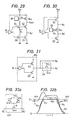
- the voltage converter to be used in the indirect peripheral circuit corresponds thereto.
- Figs. 29 and 30 show examples thereof, in which the enhancement type MOST Q LL having its gate connected with the voltage dividing means 32 is inserted in place of the depletion type MOSTs Q DN of Figs. 14 and 15, respectively. Either of these circuits converts the input pulses ⁇ 1 having the amplitude V cc into the pulse signals ⁇ 0 ' having the amplitude V cc2 .
- Figs. 31 shows another voltage converter, in which a voltage limitter LM is connected in series with the output of the usual pulse generator PG thereby to generate the pulse signals ⁇ 0 ' having the amplitude V cc2 .
- the voltage limiter LM is constructed of the enhancement type MOST Q LM which has its gate fed with the voltage V LL generated by the aforementioned voltage dividing means 32.
- Fig. 32a shows another embodiment of the voltage limiter LM.
- This embodiment has better electric characteristics than those of the voltage limiter of Fig. 31. Specifically, this embodiment can operate at a higher speed because it makes use of the self-boost trap effect resulting from the gate capacitance of the MOST Q LM .
- the summary of the operations will be described with reference to Fig. 32b.
- a node A is precharged at the potential of V LL -V th by the action of an MOST Qp R .
- the pulses ⁇ 0 then rise, the potential at the point A is raised by the capacitance combination because a reversible capacitor C G is formed between the gate, and the source and drain of an MOST Q LM .
- the effective gate voltage of the MOST Q LM is raised whereas the ON resistance of the MOST Q PR is reduced so that the output pulses ⁇ 0 ' are increased with a similar rise to that of the pulses ⁇ 0 .
- the potential V A at the point A rises with the pulses ⁇ 0 ' an MOST Q DS is rendered conducting, when the potential V A exceeds the sum of the voltages V LL and V th , so that a current path is formed in the direction from the point A to the voltage V LL .
- the potential at the point A starts to drop in accordance with the time constant, which is determined by the ON resistances of the capacitor C G and the MOST Q DS , until it is stabilized at the point of the sum of the voltages V LL and V th
- the final output voltage V cc of the pulses ⁇ 0 ' is expressed by the Equation of
- the threshold voltages of the MOSTs Q DS and Q LM are set at an equal level, the values of the voltages V cc2 and V LL become identical so that the design of the V LL generating circuit can be remarkably facilitated.
- the pulses ⁇ 0 start their drop, the pulses ⁇ 0 ' likewise drop.
- the potential at the point A is dropped by the combination of the capacitor C G so that breaking time of the pulses ⁇ 0 ' is more or less delayed.
- the ON resistance of the MOST Q PR is set at a low level, the drop of the potential at the point A can be minimized, as indicated at a broken line in Fig. 32b, so that the delay can be reduced.
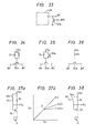
- Fig. 33 shows an example in case it is necessary to further speed up the breakdown time, and corresponds to an example in which a discharging MOST Q RS is added to the output terminal of the voltage limitter LM. According to this embodiment, it is possible to effect the break at a high speed.
- the dynamic memory all the pulses are simultaneously reset in most cases so that a resetting signal ⁇ RS can be used in common with another. However, this addition of the signal raises no special problem.
- Figs. 34 to 36 show other examples of the voltage limiter LM.
- Fig. 34 shows an example in which the MOST is replaced by diodes.
- the value of the voltage V cc2 is more or less complicated, as expressed by the Equation of but the operations are absolutely the same as those of the voltage limiter of Fig. 32.
- Fig. 35 shows an example, in which the MOST Qp R is replaced by a resistor R 4 and which is effective to improve the breakdown time.
- Fig. 36 is an example, in which the MOSTs Qp R and Q DS are replaced by a resistor R 5 and by which operations similar to those of Fig. 31 can be obtained.
- the value of the internal power source voltage V cc2 can be varied in accordance with the variation in the external power source voltage V cc so that a proper aging test can be conducted merely by varying the voltage V cc .
- the value of the voltage V cc2 is desirably held substantially constant during the usual operation and varied at a predetermined ratio to the voltage V cc only during the aging test.
- Fig. 37 shows an example of the voltage dividing means 32 for generating such voltage V cc2 .
- resistors R, and R 1 ' are set such that R 1 >>R 1 ', and a switch SW is closed only during the aging test.
- the voltage V cc2 is hardly dependent upon the voltage V cc after the point P, as shown in Fig. 37b, but the changing rate can be enlarged, as indicated at V cc2 ', just during the aging test.
- Fig. 38 shows an example, in which the switch SW is replaced by a MOST Q sw and in which the MOST Q SW also acts as the resistor R 1 '.
- ⁇ E have their voltages raised to render the MOST Q SW conducting so that the characteristics shown in Fig. 37b can be obtained.
Landscapes
- Engineering & Computer Science (AREA)
- Power Engineering (AREA)
- Microelectronics & Electronic Packaging (AREA)
- Physics & Mathematics (AREA)
- Electromagnetism (AREA)
- General Physics & Mathematics (AREA)
- Radar, Positioning & Navigation (AREA)
- Automation & Control Theory (AREA)
- Computer Hardware Design (AREA)
- Dram (AREA)
Claims (42)
Applications Claiming Priority (4)
| Application Number | Priority Date | Filing Date | Title |
|---|---|---|---|
| JP57143/81 | 1981-04-17 | ||
| JP56057143A JPS57172761A (en) | 1981-04-17 | 1981-04-17 | Semiconductor integrated circuit |
| JP168698/81 | 1981-10-23 | ||
| JP56168698A JPS5870482A (ja) | 1981-10-23 | 1981-10-23 | 半導体集積回路 |
Publications (3)
| Publication Number | Publication Date |
|---|---|
| EP0063483A2 EP0063483A2 (fr) | 1982-10-27 |
| EP0063483A3 EP0063483A3 (en) | 1984-07-25 |
| EP0063483B1 true EP0063483B1 (fr) | 1988-09-07 |
Family
ID=26398168
Family Applications (1)
| Application Number | Title | Priority Date | Filing Date |
|---|---|---|---|
| EP82301967A Expired EP0063483B1 (fr) | 1981-04-17 | 1982-04-16 | Circuit semi-conducteur intégré |
Country Status (4)
| Country | Link |
|---|---|
| US (1) | US4482985A (fr) |
| EP (1) | EP0063483B1 (fr) |
| CA (1) | CA1173519A (fr) |
| DE (1) | DE3279013D1 (fr) |
Families Citing this family (56)
| Publication number | Priority date | Publication date | Assignee | Title |
|---|---|---|---|---|
| JPS59111514A (ja) * | 1982-12-17 | 1984-06-27 | Hitachi Ltd | 半導体集積回路 |
| USRE35313E (en) * | 1981-04-17 | 1996-08-13 | Hitachi, Ltd. | Semiconductor integrated circuit with voltage limiter having different output ranges from normal operation and performing of aging tests |
| US5493572A (en) * | 1981-04-17 | 1996-02-20 | Hitachi, Ltd. | Semiconductor integrated circuit with voltage limiter having different output ranges for normal operation and performing of aging tests |
| US5566185A (en) * | 1982-04-14 | 1996-10-15 | Hitachi, Ltd. | Semiconductor integrated circuit |
| JPS59121691A (ja) * | 1982-12-01 | 1984-07-13 | Fujitsu Ltd | ダイナミツク型半導体記憶装置 |
| US4585955B1 (en) * | 1982-12-15 | 2000-11-21 | Tokyo Shibaura Electric Co | Internally regulated power voltage circuit for mis semiconductor integrated circuit |
| JPS59153331A (ja) * | 1983-02-21 | 1984-09-01 | Toshiba Corp | 半導体装置 |
| US4532467A (en) * | 1983-03-14 | 1985-07-30 | Vitafin N.V. | CMOS Circuits with parameter adapted voltage regulator |
| JPH0772852B2 (ja) * | 1984-01-26 | 1995-08-02 | 株式会社東芝 | サブミクロン半導体lsiのチップ内電源変換回路 |
| JPS60176121A (ja) * | 1984-02-22 | 1985-09-10 | Toshiba Corp | 電圧降下回路 |
| US4951251A (en) * | 1985-06-17 | 1990-08-21 | Hitachi, Ltd. | Semiconductor memory device |
| JPH07113863B2 (ja) * | 1985-06-29 | 1995-12-06 | 株式会社東芝 | 半導体集積回路装置 |
| US4873673A (en) * | 1986-12-03 | 1989-10-10 | Hitachi, Ltd. | Driver circuit having a current mirror circuit |
| US5086238A (en) * | 1985-07-22 | 1992-02-04 | Hitachi, Ltd. | Semiconductor supply incorporating internal power supply for compensating for deviation in operating condition and fabrication process conditions |
| JP2592234B2 (ja) * | 1985-08-16 | 1997-03-19 | 富士通株式会社 | 半導体装置 |
| JPH0770216B2 (ja) * | 1985-11-22 | 1995-07-31 | 株式会社日立製作所 | 半導体集積回路 |
| JPS62250593A (ja) * | 1986-04-23 | 1987-10-31 | Hitachi Ltd | ダイナミツク型ram |
| NL8702800A (nl) * | 1987-11-23 | 1989-06-16 | Philips Nv | Geintegreerde geheugenschakeling met interne voedingsspanningsregeling. |
| US5297097A (en) * | 1988-06-17 | 1994-03-22 | Hitachi Ltd. | Large scale integrated circuit for low voltage operation |
| USRE40132E1 (en) | 1988-06-17 | 2008-03-04 | Elpida Memory, Inc. | Large scale integrated circuit with sense amplifier circuits for low voltage operation |
| JPH07109864B2 (ja) * | 1989-09-13 | 1995-11-22 | シャープ株式会社 | スタティックram |
| JP2809768B2 (ja) * | 1989-11-30 | 1998-10-15 | 株式会社東芝 | 基準電位発生回路 |
| US5265056A (en) * | 1989-12-28 | 1993-11-23 | International Business Machines Corporation | Signal margin testing system for dynamic RAM |
| JPH0834709B2 (ja) * | 1990-01-31 | 1996-03-29 | 株式会社日立製作所 | 半導体集積回路及びそれを使つた電動機制御装置 |
| JP2888898B2 (ja) * | 1990-02-23 | 1999-05-10 | 株式会社日立製作所 | 半導体集積回路 |
| JPH03283562A (ja) * | 1990-03-30 | 1991-12-13 | Sony Corp | 半導体集積回路装置 |
| JP2557271B2 (ja) * | 1990-04-06 | 1996-11-27 | 三菱電機株式会社 | 内部降圧電源電圧を有する半導体装置における基板電圧発生回路 |
| US5063304A (en) * | 1990-04-27 | 1991-11-05 | Texas Instruments Incorporated | Integrated circuit with improved on-chip power supply control |
| JPH04123388A (ja) * | 1990-09-13 | 1992-04-23 | Nec Corp | 半導体メモリ装置 |
| US5103425A (en) * | 1991-03-11 | 1992-04-07 | Motorola, Inc. | Zener regulated programming circuit for a nonvolatile memory |
| JP2945508B2 (ja) * | 1991-06-20 | 1999-09-06 | 三菱電機株式会社 | 半導体装置 |
| FR2680586B1 (fr) * | 1991-08-19 | 1994-03-11 | Samsung Electronics Co Ltd | Circuit generateur de tension d'alimentation interne programmable electriquement. |
| KR940008286B1 (ko) * | 1991-08-19 | 1994-09-09 | 삼성전자 주식회사 | 내부전원발생회로 |
| JP2744738B2 (ja) * | 1992-09-07 | 1998-04-28 | 三菱電機株式会社 | 半導体記憶装置 |
| US5280420A (en) * | 1992-10-02 | 1994-01-18 | National Semiconductor Corporation | Charge pump which operates on a low voltage power supply |
| US5483152A (en) * | 1993-01-12 | 1996-01-09 | United Memories, Inc. | Wide range power supply for integrated circuits |
| KR0152905B1 (ko) * | 1994-11-15 | 1998-12-01 | 문정환 | 반도체 메모리장치의 내부전압 발생회로 |
| US5847951A (en) * | 1996-12-16 | 1998-12-08 | Dell Usa, L.P. | Method and apparatus for voltage regulation within an integrated circuit package |
| DE19716430A1 (de) * | 1997-04-18 | 1998-11-19 | Siemens Ag | Schaltungsanordnung zur Erzeugung einer internen Versorgungsspannung |
| US6150878A (en) * | 1998-01-12 | 2000-11-21 | Chip Express (Israel) Ltd. | Low voltage device operable with a high voltage supply |
| JP3621844B2 (ja) * | 1999-02-24 | 2005-02-16 | シャープ株式会社 | 増幅型固体撮像装置 |
| JP4614481B2 (ja) * | 1999-08-30 | 2011-01-19 | ルネサスエレクトロニクス株式会社 | 半導体集積回路装置 |
| US6351420B1 (en) * | 2000-02-07 | 2002-02-26 | Advanced Micro Devices, Inc. | Voltage boost level clamping circuit for a flash memory |
| AU2001282935A1 (en) | 2000-08-01 | 2002-02-13 | First Usa Bank, N.A. | System and method for transponder-enabled account transactions |
| US6329800B1 (en) | 2000-10-17 | 2001-12-11 | Sigmatel | Method and apparatus for reducing power consumption in driver circuits |
| US7526449B1 (en) | 2001-04-17 | 2009-04-28 | Jpmorgan Chase Bank N.A. | Optically encoded card and system and method for using |
| US20030019942A1 (en) * | 2001-07-24 | 2003-01-30 | Blossom George W. | System and method for electronically readable card having power source |
| US7099850B1 (en) | 2001-09-21 | 2006-08-29 | Jpmorgan Chase Bank, N.A. | Methods for providing cardless payment |
| WO2003077080A2 (fr) | 2002-03-08 | 2003-09-18 | Jp Morgan Chase Bank | Systeme financier destine a un environnement economique isole |
| US8392301B1 (en) | 2002-03-08 | 2013-03-05 | Jpmorgan Chase Bank, N.A. | Financial system for isolated economic environment |
| US20040210498A1 (en) * | 2002-03-29 | 2004-10-21 | Bank One, National Association | Method and system for performing purchase and other transactions using tokens with multiple chips |
| TW200532701A (en) * | 2003-12-18 | 2005-10-01 | Rohm Co Ltd | Semiconductor device |
| US7292088B2 (en) * | 2004-05-19 | 2007-11-06 | International Rectifier Corporation | Gate driver output stage with bias circuit for high and wide operating voltage range |
| JP4717692B2 (ja) * | 2006-04-14 | 2011-07-06 | ルネサスエレクトロニクス株式会社 | リミッタ回路 |
| USD636021S1 (en) | 2008-07-17 | 2011-04-12 | Jpmorgan Chase Bank, N.A. | Eco-friendly transaction device |
| US9583479B1 (en) * | 2016-01-14 | 2017-02-28 | Globalfoundries Inc. | Semiconductor charge pump with imbedded capacitor |
Family Cites Families (2)
| Publication number | Priority date | Publication date | Assignee | Title |
|---|---|---|---|---|
| DE2855724A1 (de) * | 1978-12-22 | 1980-07-03 | Ibm Deutschland | Verfahren und vorrichtung zur angleichung der unterschiedlichen signalverzoegerungszeiten von halbleiterchips |
| JPS5619676A (en) * | 1979-07-26 | 1981-02-24 | Fujitsu Ltd | Semiconductor device |
-
1982
- 1982-04-14 US US06/368,162 patent/US4482985A/en not_active Expired - Lifetime
- 1982-04-16 EP EP82301967A patent/EP0063483B1/fr not_active Expired
- 1982-04-16 DE DE8282301967T patent/DE3279013D1/de not_active Expired
- 1982-04-19 CA CA000401238A patent/CA1173519A/fr not_active Expired
Also Published As
| Publication number | Publication date |
|---|---|
| EP0063483A3 (en) | 1984-07-25 |
| DE3279013D1 (en) | 1988-10-13 |
| US4482985A (en) | 1984-11-13 |
| EP0063483A2 (fr) | 1982-10-27 |
| CA1173519A (fr) | 1984-08-28 |
Similar Documents
| Publication | Publication Date | Title |
|---|---|---|
| EP0063483A2 (fr) | Circuit semi-conducteur intégré | |
| US6288967B2 (en) | Semiconductor integrated circuit device | |
| KR100499452B1 (ko) | 다이나믹형메모리 | |
| US6292015B1 (en) | Semiconductor integrated circuit device including logic gate that attains reduction of power consumption and high-speed operation | |
| JP3674874B2 (ja) | 半導体集積回路のワード線昇圧回路及びその制御回路 | |
| US6046956A (en) | Semiconductor device, word line driver circuit and word line driving method | |
| KR0149577B1 (ko) | 반도체 메모리 장치의 내부 전원전압 발생회로 | |
| US5398207A (en) | MOS random access memory device with an internal voltage-down converting transistor | |
| JP2596685B2 (ja) | メモリ装置 | |
| JPH0248998B2 (fr) | ||
| JPH0249513B2 (fr) | ||
| US6674112B1 (en) | Semiconductor integrated circuit device | |
| JP4125540B2 (ja) | 半導体装置 | |
| US6603685B2 (en) | Semiconductor integrated circuit device capable of ensuring reliability of transistor driving high voltage | |
| US6847536B1 (en) | Semiconductor memory device having structure for preventing level of boosting voltage applied to a node from dropping and method of forming the same | |
| JPH0713875B2 (ja) | 半導体集積回路 | |
| JP2000101045A (ja) | 半導体装置 | |
| KR100600461B1 (ko) | 반도체 장치 | |
| JPH056665A (ja) | 大規模集積回路 | |
| JPH0793004B2 (ja) | 大規模集積回路 | |
| JPH0559518B2 (fr) | ||
| JPH052881A (ja) | 大規模集積回路 | |
| JPH0793005B2 (ja) | 大規模集積回路 | |
| JPH11297957A (ja) | 半導体記憶装置 | |
| JPH04163785A (ja) | 半導体記憶装置 |
Legal Events
| Date | Code | Title | Description |
|---|---|---|---|
| PUAI | Public reference made under article 153(3) epc to a published international application that has entered the european phase |
Free format text: ORIGINAL CODE: 0009012 |
|
| 17P | Request for examination filed |
Effective date: 19820526 |
|
| AK | Designated contracting states |
Designated state(s): DE FR GB NL |
|
| PUAL | Search report despatched |
Free format text: ORIGINAL CODE: 0009013 |
|
| AK | Designated contracting states |
Designated state(s): DE FR GB NL |
|
| 17Q | First examination report despatched |
Effective date: 19870804 |
|
| GRAA | (expected) grant |
Free format text: ORIGINAL CODE: 0009210 |
|
| AK | Designated contracting states |
Kind code of ref document: B1 Designated state(s): DE FR GB NL |
|
| REF | Corresponds to: |
Ref document number: 3279013 Country of ref document: DE Date of ref document: 19881013 |
|
| ET | Fr: translation filed | ||
| PLBE | No opposition filed within time limit |
Free format text: ORIGINAL CODE: 0009261 |
|
| STAA | Information on the status of an ep patent application or granted ep patent |
Free format text: STATUS: NO OPPOSITION FILED WITHIN TIME LIMIT |
|
| 26N | No opposition filed | ||
| PGFP | Annual fee paid to national office [announced via postgrant information from national office to epo] |
Ref country code: GB Payment date: 20010326 Year of fee payment: 20 |
|
| PGFP | Annual fee paid to national office [announced via postgrant information from national office to epo] |
Ref country code: FR Payment date: 20010418 Year of fee payment: 20 |
|
| PGFP | Annual fee paid to national office [announced via postgrant information from national office to epo] |
Ref country code: NL Payment date: 20010430 Year of fee payment: 20 |
|
| PGFP | Annual fee paid to national office [announced via postgrant information from national office to epo] |
Ref country code: DE Payment date: 20010626 Year of fee payment: 20 |
|
| REG | Reference to a national code |
Ref country code: GB Ref legal event code: IF02 |
|
| PG25 | Lapsed in a contracting state [announced via postgrant information from national office to epo] |
Ref country code: GB Free format text: LAPSE BECAUSE OF EXPIRATION OF PROTECTION Effective date: 20020415 |
|
| PG25 | Lapsed in a contracting state [announced via postgrant information from national office to epo] |
Ref country code: NL Free format text: LAPSE BECAUSE OF EXPIRATION OF PROTECTION Effective date: 20020416 |
|
| REG | Reference to a national code |
Ref country code: GB Ref legal event code: PE20 Effective date: 20020415 |
|
| NLV7 | Nl: ceased due to reaching the maximum lifetime of a patent |
Effective date: 20020416 |