EP0067566A2 - Integrierter Lichtdetektor oder -generator mit Verstärker - Google Patents
Integrierter Lichtdetektor oder -generator mit Verstärker Download PDFInfo
- Publication number
- EP0067566A2 EP0067566A2 EP82302666A EP82302666A EP0067566A2 EP 0067566 A2 EP0067566 A2 EP 0067566A2 EP 82302666 A EP82302666 A EP 82302666A EP 82302666 A EP82302666 A EP 82302666A EP 0067566 A2 EP0067566 A2 EP 0067566A2
- Authority
- EP
- European Patent Office
- Prior art keywords
- layers
- layer
- source
- integrated
- drain
- Prior art date
- Legal status (The legal status is an assumption and is not a legal conclusion. Google has not performed a legal analysis and makes no representation as to the accuracy of the status listed.)
- Ceased
Links
Images

Classifications
-
- H—ELECTRICITY
- H10—SEMICONDUCTOR DEVICES; ELECTRIC SOLID-STATE DEVICES NOT OTHERWISE PROVIDED FOR
- H10F—INORGANIC SEMICONDUCTOR DEVICES SENSITIVE TO INFRARED RADIATION, LIGHT, ELECTROMAGNETIC RADIATION OF SHORTER WAVELENGTH OR CORPUSCULAR RADIATION
- H10F99/00—Subject matter not provided for in other groups of this subclass
-
- H—ELECTRICITY
- H10—SEMICONDUCTOR DEVICES; ELECTRIC SOLID-STATE DEVICES NOT OTHERWISE PROVIDED FOR
- H10F—INORGANIC SEMICONDUCTOR DEVICES SENSITIVE TO INFRARED RADIATION, LIGHT, ELECTROMAGNETIC RADIATION OF SHORTER WAVELENGTH OR CORPUSCULAR RADIATION
- H10F39/00—Integrated devices, or assemblies of multiple devices, comprising at least one element covered by group H10F30/00, e.g. radiation detectors comprising photodiode arrays
- H10F39/10—Integrated devices
- H10F39/103—Integrated devices the at least one element covered by H10F30/00 having potential barriers, e.g. integrated devices comprising photodiodes or phototransistors
Definitions
- This invention relates to integrated light detection or generating means and amplifying means and more particularly to light sources such as light emitting diodes, or light detectors such as photodiodes integrated with amplifiers such as field effect transistors, resistors and capacitors in various group III-V multilayer structures to form a monolithic structure.
- light used herein includes invisible light such as infra-red and ultra violet.
- integrated light detecting or generating means and amplifying means comprises a field effect transistor comprising a semi-insulating substrate on which are formed source and drain layers separated by a groove, a gate layer formed in the groove bridging the source and drain layers, and further layers forming light detecting or generating means to form a monolithic structure.
- the further layers maybe directly formed on the substrate but are preferably formed on the gate layer.
- the further layers preferably define a light detector such as a photo-diode.
- the further layers may define a light source such as a light emitting diode.
- the source and drain layers preferably each comprise a buffer layer, high conductivity source and drain layers and a high resistance cover layer.
- the light detector comprises a p-n photo- diode consisting of p-type layers formed on the gate layer.
- the groove between the source and drain layers is V shaped and the gate layer and the photodiode layers are formed in the groove.
- the invention also comprises a method of making integrated light detecting or generating means and amplifying means comprising the steps of forming an FET high conductivity source/drain layer on a substrate, forming a groove in the layer produced to divide the layer into two parts, producing an FET gate layer in the groove to bridge the two layers and producing further layers forming light detecting or generating means.
- the FET high conductivity source/drain layer is preferably formed by a first epitaxial growth step, and the FET gate layer and the further layers are preferably formed by a second epitaxial growth step.
- the groove is preferably V shaped and formed by etching.
- FIG. 1 A method of making simultaneously a photodiode and a short gate junction FET on a semi-insulating InP substrate 16 is illustrated in Figures 1 to 3.
- An FET buffer layer 10, a high conductivity n + source/drain layer 12 and a high resistance n type cover layer 14 are grown in a single expitaxial growth step.
- the layer sequence is shown-in Figure 1.
- the layer 14 is then covered by a layer of photoresist 18 and slot 20 of ⁇ 1 ⁇ m is opened in the layer 18.
- the layers 10, 12 and 14 are then etched using a crystal orientation dependent etch to produce a V groove 22 to a depth such that the apex of the V groove divides the high conductivity n source/drain contact layer 12. See figure 2.
- the remainder of the photoresist layer is then removed and in a second epitaxial growth step the following layers are deposited:- an n type GaInAs layer 24, a p type GaInAs layer 26 and a p type InP layer 28. These are deposited confdrmally so that the GaInAs layer 24 bridges the gap in the n layer 12.
- Carefully controlled depth etching through photoresist patterns is performed to define a source 30, a drain 32 and a gate 34 and to define a separate p-n/ diode 36 either detached from the FET or on top of it as part of the gate as shown in Figure 3.
- An insulating layer e.g. SiO 2 (not shown) is deposited, windows opened by photoengraving and n and p type metallisations applied using engraving and float- off techniques.
- the oxide is needed to isolate interconnections and these are taken over appropriate mesa edges to preserve electrical continuity.
- the 'V' groove infilled gate FET has short (submicron) gate lengths so that high gm's result.
- the thin n FET layer 24 is controllably infilled so that the high conductivity materials necessary for high gm may be utilised.
- the infilled FET layer 24 is GaInAs which has excellent transport properties for FET's.
- the important gate/drain and gate/source capacitances which are likely to be higher than that of a MESFET may be reduced because of the high resistance layer grown onto the source/drain n LAYER 12.
- the gate junction infill 34 forms a detector in itself whose geometry can be tailored to that required for good optical coupling.
- Detection out to 1.6 ⁇ m can be achieved in the heterostructure detection layer.
- the detector diode structure is ppnin which behaves as a p-i-n- structure once the central n and i layers 12, 14 have been fully depleted.
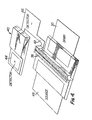
- Figure 4 illustrates a junction FET 38 integrated with a separate detector diode 40, the detector being connected to the gate of the FET by a metallic conductor 42.
- Metallic contact pads 44, 46, 48, 50 are provided for the input and output to the diode and the source and drain of the FET
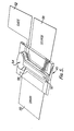
- Figure 5 illustrates a junction FET 52 integrated with a photodiode 54 which is mounted directly on the gate 56 of the FET. Again contact pads 58, 60 are provided for the source and drain, and a further contact pad 62 is provided which is connected to the gate of the FET.
Landscapes
- Solid State Image Pick-Up Elements (AREA)
- Light Receiving Elements (AREA)
- Photo Coupler, Interrupter, Optical-To-Optical Conversion Devices (AREA)
- Led Devices (AREA)
Applications Claiming Priority (2)
| Application Number | Priority Date | Filing Date | Title |
|---|---|---|---|
| GB8118258 | 1981-06-13 | ||
| GB8118258 | 1981-06-13 |
Publications (2)
| Publication Number | Publication Date |
|---|---|
| EP0067566A2 true EP0067566A2 (de) | 1982-12-22 |
| EP0067566A3 EP0067566A3 (de) | 1985-08-07 |
Family
ID=10522496
Family Applications (1)
| Application Number | Title | Priority Date | Filing Date |
|---|---|---|---|
| EP82302666A Ceased EP0067566A3 (de) | 1981-06-13 | 1982-05-25 | Integrierter Lichtdetektor oder -generator mit Verstärker |
Country Status (12)
| Country | Link |
|---|---|
| US (1) | US4625225A (de) |
| EP (1) | EP0067566A3 (de) |
| JP (1) | JPS5837956A (de) |
| KR (1) | KR840000986A (de) |
| AU (1) | AU556044B2 (de) |
| GB (1) | GB2101807B (de) |
| IN (1) | IN156696B (de) |
| KE (1) | KE3537A (de) |
| MY (1) | MY8600137A (de) |
| PT (1) | PT75043B (de) |
| SG (1) | SG32585G (de) |
| ZA (1) | ZA823971B (de) |
Cited By (8)
| Publication number | Priority date | Publication date | Assignee | Title |
|---|---|---|---|---|
| DE3300986A1 (de) * | 1982-01-18 | 1983-07-28 | Western Electric Co., Inc., 10038 New York, N.Y. | Mehrschichtige optische integrierte schaltung |
| DE3513196A1 (de) * | 1984-04-17 | 1985-10-17 | Olympus Optical Co., Ltd., Tokio/Tokyo | Festkoerper-bildsensor |
| GB2172747A (en) * | 1985-03-20 | 1986-09-24 | Int Standard Electric Corp | Junction field-effect transistor with self-aligning gate |
| DE3629681A1 (de) * | 1986-09-01 | 1988-03-10 | Licentia Gmbh | Photoempfaenger |
| EP0450827A1 (de) * | 1990-04-02 | 1991-10-09 | AT&T Corp. | Silizium-Photodiode für monolithisch integrierte Schaltungen und Herstellungsverfahren |
| US5239193A (en) * | 1990-04-02 | 1993-08-24 | At&T Bell Laboratories | Silicon photodiode for monolithic integrated circuits |
| EP2752877A4 (de) * | 2011-09-02 | 2015-07-01 | Hoon Kim | Einheitspixel und lichtempfangselement für einen bildsensor |
| US9735189B2 (en) | 2015-01-15 | 2017-08-15 | Hoon Kim | Image sensor with solar cell function and electronic device thereof |
Families Citing this family (20)
| Publication number | Priority date | Publication date | Assignee | Title |
|---|---|---|---|---|
| DE3230945A1 (de) * | 1982-08-20 | 1984-02-23 | Telefunken electronic GmbH, 7100 Heilbronn | Verfahren zum herstellen eines feldeffekttransistors |
| GB2145279B (en) * | 1983-08-18 | 1987-10-21 | Standard Telephones Cables Ltd | Photodetector integrated circuit |
| JPS6161457A (ja) * | 1984-09-01 | 1986-03-29 | Canon Inc | 光センサおよびその製造方法 |
| US5268309A (en) * | 1984-09-01 | 1993-12-07 | Canon Kabushiki Kaisha | Method for manufacturing a photosensor |
| JPS6161441A (ja) * | 1984-09-03 | 1986-03-29 | Toshiba Corp | 半導体装置の製造方法 |
| US4771325A (en) * | 1985-02-11 | 1988-09-13 | American Telephone & Telegraph Co., At&T Bell Laboratories | Integrated photodetector-amplifier device |
| DE3706252A1 (de) * | 1986-02-28 | 1987-09-03 | Canon Kk | Halbleiterfotosensor |
| US4824804A (en) * | 1986-08-15 | 1989-04-25 | American Telephone And Telegraph Company, At&T Bell Laboratories | Method of making vertical enhancement-mode group III-V compound MISFETS |
| US4962409A (en) * | 1987-01-20 | 1990-10-09 | International Business Machines Corporation | Staggered bandgap gate field effect transistor |
| JPS63276267A (ja) * | 1987-05-08 | 1988-11-14 | Fujitsu Ltd | 半導体装置の製造方法 |
| US4952017A (en) * | 1989-03-14 | 1990-08-28 | At&T Bell Laboratories | Polarization independent semiconductor optical amplifier |
| US4970386A (en) * | 1989-06-22 | 1990-11-13 | Westinghouse Electric Corp. | Vertical FET high speed optical sensor |
| US6548878B1 (en) | 1998-02-05 | 2003-04-15 | Integration Associates, Inc. | Method for producing a thin distributed photodiode structure |
| US6303967B1 (en) | 1998-02-05 | 2001-10-16 | Integration Associates, Inc. | Process for producing an isolated planar high speed pin photodiode |
| US6458619B1 (en) | 1998-02-05 | 2002-10-01 | Integration Associates, Inc. | Process for producing an isolated planar high speed pin photodiode with improved capacitance |
| US6027956A (en) * | 1998-02-05 | 2000-02-22 | Integration Associates, Inc. | Process for producing planar dielectrically isolated high speed pin photodiode |
| US6753586B1 (en) | 1998-03-09 | 2004-06-22 | Integration Associates Inc. | Distributed photodiode structure having majority dopant gradient and method for making same |
| US6690078B1 (en) | 1999-08-05 | 2004-02-10 | Integration Associates, Inc. | Shielded planar dielectrically isolated high speed pin photodiode and method for producing same |
| JP2007516607A (ja) * | 2003-05-29 | 2007-06-21 | アプライド マテリアルズ インコーポレイテッド | 埋込式導波路検出器 |
| DE10350643B4 (de) * | 2003-10-29 | 2008-12-04 | Infineon Technologies Ag | Verfahren zur Herstellung einer antireflektierenden Oberfläche auf optischen integrierten Schaltkreisen |
Family Cites Families (7)
| Publication number | Priority date | Publication date | Assignee | Title |
|---|---|---|---|---|
| US4075651A (en) * | 1976-03-29 | 1978-02-21 | Varian Associates, Inc. | High speed fet employing ternary and quarternary iii-v active layers |
| JPS53118988A (en) * | 1977-03-28 | 1978-10-17 | Nippon Gakki Seizo Kk | Integrated circuit device and its manufacture |
| US4173765A (en) * | 1978-05-26 | 1979-11-06 | Eastman Kodak Company | V-MOS imaging array |
| US4212020A (en) * | 1978-07-21 | 1980-07-08 | California Institute Of Technology | Solid state electro-optical devices on a semi-insulating substrate |
| JPS55117295A (en) * | 1979-03-02 | 1980-09-09 | Hitachi Ltd | Semiconductor light emitting element and fabricating the same |
| JPS55128884A (en) * | 1979-03-28 | 1980-10-06 | Hitachi Ltd | Semiconductor photodetector |
| US4274104A (en) * | 1979-05-21 | 1981-06-16 | International Business Machines Corporation | Electrooptical integrated circuit communication |
-
1982
- 1982-05-25 EP EP82302666A patent/EP0067566A3/de not_active Ceased
- 1982-06-01 GB GB08215957A patent/GB2101807B/en not_active Expired
- 1982-06-07 ZA ZA823971A patent/ZA823971B/xx unknown
- 1982-06-09 PT PT75043A patent/PT75043B/pt unknown
- 1982-06-10 AU AU84758/82A patent/AU556044B2/en not_active Ceased
- 1982-06-11 KR KR1019820002602A patent/KR840000986A/ko not_active Abandoned
- 1982-06-11 IN IN675/CAL/82A patent/IN156696B/en unknown
- 1982-06-11 JP JP57099445A patent/JPS5837956A/ja active Pending
- 1982-06-11 US US06/387,348 patent/US4625225A/en not_active Expired - Fee Related
-
1985
- 1985-05-02 SG SG325/85A patent/SG32585G/en unknown
- 1985-05-21 KE KE3537A patent/KE3537A/xx unknown
-
1986
- 1986-12-30 MY MY137/86A patent/MY8600137A/xx unknown
Cited By (13)
| Publication number | Priority date | Publication date | Assignee | Title |
|---|---|---|---|---|
| DE3300986A1 (de) * | 1982-01-18 | 1983-07-28 | Western Electric Co., Inc., 10038 New York, N.Y. | Mehrschichtige optische integrierte schaltung |
| DE3513196A1 (de) * | 1984-04-17 | 1985-10-17 | Olympus Optical Co., Ltd., Tokio/Tokyo | Festkoerper-bildsensor |
| GB2172747A (en) * | 1985-03-20 | 1986-09-24 | Int Standard Electric Corp | Junction field-effect transistor with self-aligning gate |
| DE3629681A1 (de) * | 1986-09-01 | 1988-03-10 | Licentia Gmbh | Photoempfaenger |
| EP0450827A1 (de) * | 1990-04-02 | 1991-10-09 | AT&T Corp. | Silizium-Photodiode für monolithisch integrierte Schaltungen und Herstellungsverfahren |
| US5141878A (en) * | 1990-04-02 | 1992-08-25 | At&T Bell Laboratories | Silicon photodiode for monolithic integrated circuits and method for making same |
| US5239193A (en) * | 1990-04-02 | 1993-08-24 | At&T Bell Laboratories | Silicon photodiode for monolithic integrated circuits |
| EP2752877A4 (de) * | 2011-09-02 | 2015-07-01 | Hoon Kim | Einheitspixel und lichtempfangselement für einen bildsensor |
| US9735189B2 (en) | 2015-01-15 | 2017-08-15 | Hoon Kim | Image sensor with solar cell function and electronic device thereof |
| US9735188B2 (en) | 2015-01-15 | 2017-08-15 | Hoon Kim | Image sensor with solar cell function |
| US9985057B2 (en) | 2015-01-15 | 2018-05-29 | Hoon Kim | Image sensor with solar cell function and electronic device thereof |
| US9997549B2 (en) | 2015-01-15 | 2018-06-12 | Hoon Kim | Image sensor with solar cell function and electronic device thereof |
| US10020329B2 (en) | 2015-01-15 | 2018-07-10 | Hoon Kim | Image sensor with solar cell function |
Also Published As
| Publication number | Publication date |
|---|---|
| GB2101807A (en) | 1983-01-19 |
| SG32585G (en) | 1985-11-15 |
| JPS5837956A (ja) | 1983-03-05 |
| ZA823971B (en) | 1983-04-27 |
| EP0067566A3 (de) | 1985-08-07 |
| MY8600137A (en) | 1986-12-31 |
| US4625225A (en) | 1986-11-25 |
| PT75043A (en) | 1982-07-01 |
| KR840000986A (ko) | 1984-03-26 |
| AU556044B2 (en) | 1986-10-23 |
| PT75043B (en) | 1984-02-17 |
| KE3537A (en) | 1985-06-07 |
| IN156696B (de) | 1985-10-19 |
| GB2101807B (en) | 1985-02-20 |
| AU8475882A (en) | 1982-12-23 |
Similar Documents
| Publication | Publication Date | Title |
|---|---|---|
| EP0067566A2 (de) | Integrierter Lichtdetektor oder -generator mit Verstärker | |
| US4884119A (en) | Integrated multiple quantum well photonic and electronic devices | |
| US4956682A (en) | Optoelectronic integrated circuit | |
| US4761383A (en) | Method of manufacturing avalanche photo diode | |
| US4847665A (en) | Monolithic integration of optoelectronic and electronic devices | |
| US6583482B2 (en) | Hetero-interface avalance photodetector | |
| US5357127A (en) | Pin heterojunction photo diode with undercut gate jifet | |
| US5684819A (en) | Monolithically integrated circuits having dielectrically isolated, electrically controlled optical devices | |
| GB2168528A (en) | PIN-diode and FET | |
| US5104823A (en) | Monolithic integration of optoelectronic and electronic devices | |
| US4505765A (en) | Manufacturing method for a planar photodiode with hetero-structure | |
| JPH01109764A (ja) | 光電子集積回路 | |
| GB2240874A (en) | Photodiode | |
| JPS6360562A (ja) | 光半導体装置の製造方法 | |
| JP2711055B2 (ja) | 半導体光検出器およびその製造方法 | |
| JPH03291968A (ja) | 光電子集積回路の製造方法 | |
| JPH0316275A (ja) | 半導体受光素子の製造方法 | |
| KR960015270B1 (ko) | 수신용 단일칩 광전집적회로의 반도체 제조방법 | |
| Liao et al. | A planar embedded InGaAs photodiode on semi-insulating InP substrate for monolithically integrated PIN-FET receivers, using selective vapor phase epitaxy and ion implantation technique | |
| JPS59222988A (ja) | 化合物半導体素子およびその製造方法 | |
| JPH05218379A (ja) | 光・電子集積回路装置 | |
| JPH01296663A (ja) | 光電子集積回路 | |
| JPS6344789A (ja) | 半導体レ−ザ装置 | |
| JPH021979A (ja) | 光電子集積回路の製造方法 | |
| JPS63158871A (ja) | 光・電子集積回路 |
Legal Events
| Date | Code | Title | Description |
|---|---|---|---|
| PUAI | Public reference made under article 153(3) epc to a published international application that has entered the european phase |
Free format text: ORIGINAL CODE: 0009012 |
|
| AK | Designated contracting states |
Designated state(s): CH DE FR IT LI SE |
|
| 17P | Request for examination filed |
Effective date: 19821123 |
|
| PUAL | Search report despatched |
Free format text: ORIGINAL CODE: 0009013 |
|
| AK | Designated contracting states |
Designated state(s): CH DE FR IT LI SE |
|
| 17Q | First examination report despatched |
Effective date: 19870522 |
|
| STAA | Information on the status of an ep patent application or granted ep patent |
Free format text: STATUS: THE APPLICATION HAS BEEN REFUSED |
|
| 18R | Application refused |
Effective date: 19880208 |
|
| RIN1 | Information on inventor provided before grant (corrected) |
Inventor name: GOODFELLOW, ROBERT CHARLES Inventor name: CARTER, ANDREW CANNON |