EP0068630A1 - Elektrolumineszierende Anzeigevorrichtung - Google Patents
Elektrolumineszierende Anzeigevorrichtung Download PDFInfo
- Publication number
- EP0068630A1 EP0068630A1 EP82302634A EP82302634A EP0068630A1 EP 0068630 A1 EP0068630 A1 EP 0068630A1 EP 82302634 A EP82302634 A EP 82302634A EP 82302634 A EP82302634 A EP 82302634A EP 0068630 A1 EP0068630 A1 EP 0068630A1
- Authority
- EP
- European Patent Office
- Prior art keywords
- voltage
- display element
- electroluminescent display
- diode
- transistor
- Prior art date
- Legal status (The legal status is an assumption and is not a legal conclusion. Google has not performed a legal analysis and makes no representation as to the accuracy of the status listed.)
- Granted
Links
Images

Classifications
-
- G—PHYSICS
- G09—EDUCATION; CRYPTOGRAPHY; DISPLAY; ADVERTISING; SEALS
- G09F—DISPLAYING; ADVERTISING; SIGNS; LABELS OR NAME-PLATES; SEALS
- G09F13/00—Illuminated signs; Luminous advertising
- G09F13/20—Illuminated signs; Luminous advertising with luminescent surfaces or parts
- G09F13/22—Illuminated signs; Luminous advertising with luminescent surfaces or parts electroluminescent
-
- G—PHYSICS
- G09—EDUCATION; CRYPTOGRAPHY; DISPLAY; ADVERTISING; SEALS
- G09G—ARRANGEMENTS OR CIRCUITS FOR CONTROL OF INDICATING DEVICES USING STATIC MEANS TO PRESENT VARIABLE INFORMATION
- G09G3/00—Control arrangements or circuits, of interest only in connection with visual indicators other than cathode-ray tubes
- G09G3/20—Control arrangements or circuits, of interest only in connection with visual indicators other than cathode-ray tubes for presentation of an assembly of a number of characters, e.g. a page, by composing the assembly by combination of individual elements arranged in a matrix no fixed position being assigned to or needed to be assigned to the individual characters or partial characters
- G09G3/22—Control arrangements or circuits, of interest only in connection with visual indicators other than cathode-ray tubes for presentation of an assembly of a number of characters, e.g. a page, by composing the assembly by combination of individual elements arranged in a matrix no fixed position being assigned to or needed to be assigned to the individual characters or partial characters using controlled light sources
- G09G3/30—Control arrangements or circuits, of interest only in connection with visual indicators other than cathode-ray tubes for presentation of an assembly of a number of characters, e.g. a page, by composing the assembly by combination of individual elements arranged in a matrix no fixed position being assigned to or needed to be assigned to the individual characters or partial characters using controlled light sources using electroluminescent panels
-
- G—PHYSICS
- G09—EDUCATION; CRYPTOGRAPHY; DISPLAY; ADVERTISING; SEALS
- G09F—DISPLAYING; ADVERTISING; SIGNS; LABELS OR NAME-PLATES; SEALS
- G09F13/00—Illuminated signs; Luminous advertising
- G09F13/20—Illuminated signs; Luminous advertising with luminescent surfaces or parts
- G09F13/22—Illuminated signs; Luminous advertising with luminescent surfaces or parts electroluminescent
- G09F2013/222—Illuminated signs; Luminous advertising with luminescent surfaces or parts electroluminescent with LEDs
-
- G—PHYSICS
- G09—EDUCATION; CRYPTOGRAPHY; DISPLAY; ADVERTISING; SEALS
- G09G—ARRANGEMENTS OR CIRCUITS FOR CONTROL OF INDICATING DEVICES USING STATIC MEANS TO PRESENT VARIABLE INFORMATION
- G09G2300/00—Aspects of the constitution of display devices
- G09G2300/08—Active matrix structure, i.e. with use of active elements, inclusive of non-linear two terminal elements, in the pixels together with light emitting or modulating elements
- G09G2300/0809—Several active elements per pixel in active matrix panels
- G09G2300/0842—Several active elements per pixel in active matrix panels forming a memory circuit, e.g. a dynamic memory with one capacitor
Definitions
- This invention relates to an electroluminescent display device.
- a device combining thin-film electroluminescent (EL) phosphor and an active matrix array driver has recently been developed in the field of display devices.
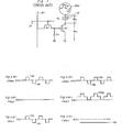
- Figure 1 of the accompanying drawings is an equivalent circuit diagram of a display element and addressing circuitry of a previously proposed EL display device which employs TFT technology.
- Figures 2(a) to 2(c) and Figures 3(a) to 3(c) of the accompanying drawings are waveform diagrams for assistance in explanation of operations of the display element and addressing circuitry of Figure 1.
- a data line DL is connected to the drain terminal of a first switching element Q 1 , constituted by a MOS FET, whilst a scanning line SL is connected to the gate terminal of the transistor Q 1 .
- the source terminal of transistor Q 1 is connected to the gate terminal of a second switching element Q 2 , constituted by a MOS FET, and is also connected to a capacitor C S for data accumulation.
- the drain terminal of the transistor Q 2 is connected to one electrode of the display element EL.
- the source terminal of transistor Q 2 is connected to a reference voltage, for example earth potential.
- the display element EL has a thin-film structure in which an EL phosphor layer el, such as ZnS:Mn, is sandwiched via insulating film (not shown) between a couple of electrodes.
- a pulsewise AC voltage is supplied to the other electrode of the display element EL, from a power'supply POW, when the device is in use.
- the voltage V EL applied across the electrodes of the display element EL is in this case a DC voltage as shown in Figure 3(c), which is the difference between V DS and the pulsewise AC supply voltage.
- the transistor Q 2 is "OFF"
- the AC driven type display element EL does not emit light.
- an electroluminescent display device comprising:
- An embodiment of the present invention can provide technical matching between an EL display element, which requires comparatively high drive voltage, and active switching elements having a low breakdown voltage, when an active matrix addressing circuit and EL display elements are combined.
- An embodiment of the present invention can provide 'for the protection of a MOS switching element from non-recoverable breakdown when employed with a display element needing a high drive voltage, using only a simple structure.
- An embodiment of the present invention can provide a MOS-EL integrated display device using a silicon substrate which can be fabricated easily and which offers high reliability.
- An embodiment of the present invention can provide a MOS-EL integrated display device in which protection is afforded for an MOS switching element which forms part of an active matrix which is combined with EL display elements in the device.
- the breakdown voltage provided by a p- n junction associated with a switching transistor element connected to an EL display element is set to the difference between a luminous voltage (a voltage which, when applied to the display element, causes the display element to be visibly luminous) and a non-luminous voltage (a voltage which, when applied to the display element, is not sufficient to cause the display element to be visibly luminous), and an OFF voltage, which is applied to the switching transistor element when the display element is not visibly luminous, is clamped to a voltage such that non-recoverable breakdown of the switching transistor element cannot occur.
- a luminous voltage a voltage which, when applied to the display element, causes the display element to be visibly luminous
- a non-luminous voltage a voltage which, when applied to the display element, is not sufficient to cause the display element to be visibly luminous
- an OFF voltage which is applied to the switching transistor element when the display element is not visibly luminous
- An EL display device embodying the present invention comprises a semiconductor substrate, and a plurality of display electrodes, corresponding to display picture elements arranged on the semiconductor substrate with an EL layer disposed between each display electrode and an opposing electrode, and moreover comprises, on the semiconductor substrate, a plurality of switching transistor elements each for selective drive of a display electrode and each connected to a respective display electrode, with a p-n junction formed between the transistor electrode connected to the display electrode and the semiconductor substrate, the p-n junction having a breakdown voltage equal to the difference between a luminous voltage and a non-luminous voltage of the EL layer.
- Each p-n junction constitutes a Zener diode connected in parallel to the switching transistor element concerned and clamps.the voltage across the transistor element in the OFF state to the non-recoverable breakdown voltage of the relevant element or to a lower voltage.
- each such p-n junction which functions as a Zener diode is formed as the junction between the drain region of a switching MOS transistor element and the substrate.
- a diode element formed independently of a switching transistor element can be integrated for this purpose.
- the breakdown voltage of each p-n junction is preferably set to a voltage larger than the difference between a luminous voltage and a maximum non-luminous voltage so that thereby the EL-display element can be biased to a voltage lower than the maximum non-luminous voltage in the OFF condition.
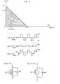
- a typical voltage-brightness characteristic curve of a thin-film EL display element is shown in the graph of Figure 4.
- the thin-film EL display element will not be of sufficient brightness to be perceived by the eye even when the voltage applied to the display element reaches a comparatively high level V NA .
- the display element has a characteristic such that its brightness increases sharply, from B1 to B2, with a relatively small increase in applied voltage from V NA to V A .
- the display element can be considered to be in a non-luminous condition or OFF state with a brightness level of B1 - this level generally corresponds to about 1fL - and a voltage V NA which gives such a brightness level B1 can be considered to be a display threshold voltage or a maximum non-luminous voltage.
- voltages up to V NA can be defined as non-luminous voltages or OFF voltages V OFF .
- brightness level B2 - a level generally of 20fL or higher - corresponds to a luminous condition or ON state of the display element and a voltage V A which gives such a brightness level B2 can be defined as a luminous voltage or ON voltage V ON .
- an embodiment of the present invention operates so that a non-luminous voltage V OFF' up to V NA , is applied to the display element when it is in an OFF state (when no luminous display is to be provided thereby) and so that ON-OFF status of the display element is controlled by switching of a voltage corresponding to the difference between luminous voltage V ON and non-luminous voltage v OFF , using a transistor for selective drive of the display element.
- an embodiment of the present invention provides a clamping diode having a breakdown voltage V z which satisfies the relationship V Z ⁇ V A -V NA in parallel to a transistor, for selective drive of the display element, which is connected in series with the EL display element.
- Figure 5 schematically shows a sectional view of an N channel MOS transistor as used in an embodiment of the present invention, in place of the TFT type switching transistor Q 2 shown in Figure 1.
- 11 is a p-TYPE SILICON substrate
- 12 is a source region
- S is a source terminal
- 13 is a drain region
- D is a drain terminal
- 14 is a gate insulating film
- 15 is a gate electrode
- G is a gate terminal.
- a diode D Z as shown in Figure 5 is formed at the junction between drain region 13 and substrate 11 when the source region 12 and drain region 13 are formed by diffusing n-type impurity into a p-type silicon substrate 11.
- Figure 6 shows an equivalent circuit of a display element and addressing circuitry using a transistor Q 2 as shown in Figure 5.
- the addresssing circuitry may also comprise elements corresponding to Q 1 , C S , DL and SL as shown in Figure 1, but for clarity these are not shown in Figure 6.
- the source terminal S and the substrate of the transistor Q 2 are grounded (as indicated in Figure 5), and the drain terminal D is connected to the display element EL.
- the diode D Z cannot be ignored, as mentioned above, and the display element EL can be thought of as being grounded via the backward diode D Z , and a clamping function provided by means of the constant voltage characteristic of this diode D Z is utilized. That is, when the transistor Q 2 is OFF, the electrode of the display element that is connected to the drain terminal D can be thought of as being grounded by the diode D Z and clamped to a particular constant voltage by virtue of the constant voltage characteristic of the diode D Z .
- the diode D Z can be considered as a Zen er diode, not merely as a backward diode.
- the diode D z when reversed biased provides a breakdown voltage which clamps the drain terminal D relative to the reference potential (e.g. ground voltage) applied to the source terminal S.
- the diode D Z acts as a Zen er diode with its breakdown voltage providing a clamping level.
- Figure 7 is a graph illustrating the characteristic relationship between the drain-source voltage V DS of the drive transistor Q2 and the voltage V EL which is applied across the display element EL when the power supply POW becomes positive.
- the horizontal axis represents voltage V DS
- the vertical axis represents voltage V EL .
- V x V A -V NA
- V DS V A -V NA
- the breakdown voltage V Z can be set to a value smaller than 2VA(V), but within the operating voltage range higher than V X (V) and the display element maintained in the OFF state. It is desirable that the breakdown voltage V Z be lower rather than higher within this range for ease of fabrication, and it is preferable to set V z to a value equal to V A -V NA (as indicated in Figure 4) or a little higher.
- Figures 8(a), 8(b), and 8(c) respectively show waveforms of the power supply POW, V DS and V EL , when V Z is set to a value as indicated above and the driver transistor Q 2 is set to the "OFF" state.
- Figure 8(a) shows the waveform of the signal supplied from the power supply POW
- Figure 8(b) shows the waveform of the voltage V DS across drain and source
- Figure 8(c) shows the waveform of the voltage V EL applied across the display element EL in the OFF state.
- V z should be set to about 40V to ensure that the display element remains in an OFF state when Q 2 is OFF.
- the voltage across the transistor Q 2 (when OFF) need only be clamped to about 40V so that a breakdown voltage of 40V or a little higher is sufficient for Q 2 .
- a MOS transistor providing such breakdown voltage can be readily constituted in an integrated circuit device using practical fabrication processes.
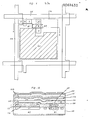
- Figure 9 and Figure 10 show part of an example of an EL display device embodying the present invention in which a plurality of EL display elements are arranged in the form of a matrix and are integrated together with active matrix driving circuitry using semiconductor fabrication techniques.
- Figure 9 is a plan view and Figure 10 is a sectional view taken along the line X-X in Figure 9.
- Figures 9 and 10 illustrate a structure corresponding items corresponding to to the circuit of Figure 6, together with/DL, SL, C S and Q 1 of Figure 1.
- 117 is a silicon substrate.
- transistors Q 1 , Q 2 , a capacitor C S and a display element EL are formed in a multi-layered structure.
- the display element EL comprises a display electrode 111a (an independent display element electrode llla is provided for each display element EL), a thin-film EL phosphor el consisting of ZnS:Mn sandwiched between insulating films lllb of, for example, Y 2 O 3 , and a transparent electrode (ITO film) 111c common to all display elements.
- a data line (DL) conductor 114 is connected to a drain terminal D of a transistor Q 1 (See Figure 1), whilst a scanning line (SL) conductor 115 is connected to the gate terminal G of transistor Q 1 (see Figure 1).
- An electrode 116 is used in common as the gate terminal G of transistor Q 2 and as one electrode of capacitor C S , which capacitor comprises electrodes 116 and 118.
- Conductor 113 functions as a shielding electrode.
- the plan view of Figure 9 shows D, G and S for each of transistors Q 1 and Q 2 , capacitor C S , a display electrode llla and conductors 114 and 115.
- a clamping diode element having a breakdown voltage is provided in the layer structure of Figure 10.
- the MOS type FET Q 2 provides a diode function between its drain and the substrate and the breakdown voltage V z of the p-n junction between drain and substrate is set to a suitable level as explained above.
- a MOS type FET Q 2 may employ either a N type or a P type channel structure, since both positive and negative (bipolar) polarity pulses are used for driving an EL display element,and the driving source voltage and the voltage V z can be controlled by adjusting impurity concentration and impurity depth when forming the drain region in the substrate.
- a MOS FET having a P type channel structure the direction of diode D Z is naturally the opposite of that shown in Figure 6.
- a bipolar transistor as a switching transistor Q 2 , instead of a MOS type FET, as shown in Figure 11(b).
- a diode element D Z1 can be connected externally, between the collector terminal C and the emitter terminal E of the bipolar transistor, to provide the specified breakdown voltage VZ.
- diode D Z1 is external of the switching transistor it can of course be provided as an element in the same integrated circuit structure as the switching transistor and the EL display element.
- the breakdown voltage required of a switching transistor can be reduced by providing a Zener diode in parallel with the switching transistor for selective driving of an EL display element and by setting the breakdown voltage Vz of the diode to the difference between a luminous voltage and a non-luminous voltage of the EL display element. Therefore, the application of embodiments of the present invention to EL display devices in which a plurality of EL display elements and an active address/driving matrix are integrated together facilitates the fabrication of for example MOS switching transistors as integrated circuit elements and can provide low cost highly reliable devices.
- embodiments of the present invention can advantageously be employed in modular type display devices, such as are proposed by T.Unotoro et al in U.S Patent Application serial No.236,621.
- An embodiment of the present invention provides a thin-film EL display device incorporating an MOS active matrix.
- Each transistor of an MOS transistor array is provided with a Zen er diode in parallel thereto for the purpose of protection from high voltages.
- Such a Zen ' er diode has a breakdown voltage characteristic corresponding to the difference between a luminous voltage and a non-luminous voltage of an EL display element and clamps the voltage across the parallel-connected MOS transistor, in the OFF state, to a value such that non-recoverable breakdown of the transistor cannot occur.
Landscapes
- Engineering & Computer Science (AREA)
- Physics & Mathematics (AREA)
- General Physics & Mathematics (AREA)
- Theoretical Computer Science (AREA)
- Computer Hardware Design (AREA)
- Electroluminescent Light Sources (AREA)
- Control Of El Displays (AREA)
- Control Of Indicators Other Than Cathode Ray Tubes (AREA)
Applications Claiming Priority (4)
| Application Number | Priority Date | Filing Date | Title |
|---|---|---|---|
| JP56080307A JPS57194483A (en) | 1981-05-25 | 1981-05-25 | El type display element driving circuit |
| JP80307/81 | 1981-05-25 | ||
| JP2963482A JPS58144893A (ja) | 1982-02-23 | 1982-02-23 | El型表示装置 |
| JP29634/82 | 1982-02-23 |
Publications (2)
| Publication Number | Publication Date |
|---|---|
| EP0068630A1 true EP0068630A1 (de) | 1983-01-05 |
| EP0068630B1 EP0068630B1 (de) | 1985-10-30 |
Family
ID=26367855
Family Applications (1)
| Application Number | Title | Priority Date | Filing Date |
|---|---|---|---|
| EP82302634A Expired EP0068630B1 (de) | 1981-05-25 | 1982-05-24 | Elektrolumineszierende Anzeigevorrichtung |
Country Status (3)
| Country | Link |
|---|---|
| US (1) | US4523189A (de) |
| EP (1) | EP0068630B1 (de) |
| DE (1) | DE3267122D1 (de) |
Cited By (1)
| Publication number | Priority date | Publication date | Assignee | Title |
|---|---|---|---|---|
| EP0701238A3 (de) * | 1994-08-19 | 1997-02-26 | Planar Systems Inc | Entwurf einer Elektrolumineszenz-Zelle für eine aktive Matrix |
Families Citing this family (34)
| Publication number | Priority date | Publication date | Assignee | Title |
|---|---|---|---|---|
| US4630893A (en) * | 1985-04-29 | 1986-12-23 | Rca Corporation | LCD pixel incorporating segmented back-to-back diode |
| US4739320A (en) * | 1985-04-30 | 1988-04-19 | Planar Systems, Inc. | Energy-efficient split-electrode TFEL panel |
| DE3782858T2 (de) * | 1986-06-17 | 1993-04-08 | Fujitsu Ltd | Ansteuerung fuer eine anzeigevorrichtung in matrix-form. |
| US5016982A (en) * | 1986-07-22 | 1991-05-21 | Raychem Corporation | Liquid crystal display having a capacitor for overvoltage protection |
| JPS63276895A (ja) * | 1987-05-08 | 1988-11-15 | Hitachi Ltd | エレクトロルミネセント素子の製造方法 |
| US4769753A (en) * | 1987-07-02 | 1988-09-06 | Minnesota Mining And Manufacturing Company | Compensated exponential voltage multiplier for electroluminescent displays |
| JP2678017B2 (ja) * | 1988-06-13 | 1997-11-17 | シャープ株式会社 | アクティブマトリクス表示装置 |
| US5051738A (en) * | 1989-02-27 | 1991-09-24 | Revtek Inc. | Imaging system |
| US5099301A (en) * | 1989-09-29 | 1992-03-24 | Yu Holding (Bvi), Inc. | Electroluminescent semiconductor device |
| JP3071851B2 (ja) * | 1991-03-25 | 2000-07-31 | 株式会社半導体エネルギー研究所 | 電気光学装置 |
| US6778231B1 (en) | 1991-06-14 | 2004-08-17 | Semiconductor Energy Laboratory Co., Ltd. | Electro-optical display device |
| US6975296B1 (en) | 1991-06-14 | 2005-12-13 | Semiconductor Energy Laboratory Co., Ltd. | Electro-optical device and method of driving the same |
| JPH08129360A (ja) * | 1994-10-31 | 1996-05-21 | Tdk Corp | エレクトロルミネセンス表示装置 |
| US5576726A (en) * | 1994-11-21 | 1996-11-19 | Motorola | Electro-luminescent display device driven by two opposite phase alternating voltages and method therefor |
| US5550066A (en) * | 1994-12-14 | 1996-08-27 | Eastman Kodak Company | Method of fabricating a TFT-EL pixel |
| US6853083B1 (en) | 1995-03-24 | 2005-02-08 | Semiconductor Energy Laboratory Co., Ltd. | Thin film transfer, organic electroluminescence display device and manufacturing method of the same |
| US5796120A (en) * | 1995-12-28 | 1998-08-18 | Georgia Tech Research Corporation | Tunnel thin film electroluminescent device |
| WO1998013811A1 (fr) * | 1996-09-26 | 1998-04-02 | Seiko Epson Corporation | Dispositif d'affichage |
| US8853696B1 (en) * | 1999-06-04 | 2014-10-07 | Semiconductor Energy Laboratory Co., Ltd. | Electro-optical device and electronic device |
| TW591584B (en) * | 1999-10-21 | 2004-06-11 | Semiconductor Energy Lab | Active matrix type display device |
| JP4869497B2 (ja) * | 2001-05-30 | 2012-02-08 | 株式会社半導体エネルギー研究所 | 表示装置 |
| JP3810725B2 (ja) * | 2001-09-21 | 2006-08-16 | 株式会社半導体エネルギー研究所 | 発光装置及び電子機器 |
| JP4024557B2 (ja) | 2002-02-28 | 2007-12-19 | 株式会社半導体エネルギー研究所 | 発光装置、電子機器 |
| TWI229774B (en) * | 2002-06-11 | 2005-03-21 | Sony Corp | Semiconductor device, reflective liquid crystal display apparatus and reflective liquid crystal projection apparatus |
| FR2846794A1 (fr) * | 2002-11-05 | 2004-05-07 | Thomson Licensing Sa | Panneau organique electroluminescent bi-stable ou chaque cellule comprend une diode de shockley |
| US6866678B2 (en) | 2002-12-10 | 2005-03-15 | Interbational Technology Center | Phototherapeutic treatment methods and apparatus |
| JP4641710B2 (ja) | 2003-06-18 | 2011-03-02 | 株式会社半導体エネルギー研究所 | 表示装置 |
| KR20050037639A (ko) * | 2003-10-20 | 2005-04-25 | 엘지전자 주식회사 | 에너지 회수장치 |
| US7595775B2 (en) * | 2003-12-19 | 2009-09-29 | Semiconductor Energy Laboratory Co., Ltd. | Light emitting display device with reverse biasing circuit |
| US8355015B2 (en) | 2004-05-21 | 2013-01-15 | Semiconductor Energy Laboratory Co., Ltd. | Semiconductor device, display device and electronic device including a diode electrically connected to a signal line |
| US20050276292A1 (en) * | 2004-05-28 | 2005-12-15 | Karl Schrodinger | Circuit arrangement for operating a laser diode |
| US7592975B2 (en) * | 2004-08-27 | 2009-09-22 | Semiconductor Energy Laboratory Co., Ltd. | Display device and driving method thereof |
| CN105742364A (zh) * | 2016-04-12 | 2016-07-06 | 中山大学 | 一种抑制有源沟道区光致漏电流产生的mos管及应用 |
| US12125446B2 (en) * | 2021-10-18 | 2024-10-22 | Microsoft Technology Licensing, Llc | Compliance voltage based on diode output brightness |
Citations (2)
| Publication number | Priority date | Publication date | Assignee | Title |
|---|---|---|---|---|
| US3522473A (en) * | 1967-12-26 | 1970-08-04 | Itt | Electroluminescent display utilizing voltage breakdown diodes |
| US4081716A (en) * | 1976-03-01 | 1978-03-28 | Ise Electronics Corporation | Fluorescent display elements |
Family Cites Families (6)
| Publication number | Priority date | Publication date | Assignee | Title |
|---|---|---|---|---|
| GB1170705A (en) * | 1967-02-27 | 1969-11-12 | Hitachi Ltd | An Insulated Gate Type Field Effect Semiconductor Device having a Breakdown Preventing Circuit Device and a method of manufacturing the same |
| US3673428A (en) * | 1970-09-18 | 1972-06-27 | Rca Corp | Input transient protection for complementary insulated gate field effect transistor integrated circuit device |
| DE2531846C2 (de) * | 1974-07-16 | 1989-12-14 | Nippon Electric Co., Ltd., Tokyo | Schutzschaltungsanordnung für einen Isolierschicht-Feldeffekttransistor |
| US3936863A (en) * | 1974-09-09 | 1976-02-03 | Rca Corporation | Integrated power transistor with ballasting resistance and breakdown protection |
| DE2645182C2 (de) * | 1976-10-07 | 1983-02-10 | Deutsche Itt Industries Gmbh, 7800 Freiburg | Temperaturkompensierte Z-Diodenanordnung, Betriebsschaltung hierfür und Verwendung der Anordnung mit dieser Betriebsschaltung |
| US4368467A (en) * | 1980-02-29 | 1983-01-11 | Fujitsu Limited | Display device |
-
1982
- 1982-05-21 US US06/380,698 patent/US4523189A/en not_active Expired - Lifetime
- 1982-05-24 DE DE8282302634T patent/DE3267122D1/de not_active Expired
- 1982-05-24 EP EP82302634A patent/EP0068630B1/de not_active Expired
Patent Citations (2)
| Publication number | Priority date | Publication date | Assignee | Title |
|---|---|---|---|---|
| US3522473A (en) * | 1967-12-26 | 1970-08-04 | Itt | Electroluminescent display utilizing voltage breakdown diodes |
| US4081716A (en) * | 1976-03-01 | 1978-03-28 | Ise Electronics Corporation | Fluorescent display elements |
Non-Patent Citations (2)
| Title |
|---|
| PROCEEDINGS OF THE SOCIETY FOR INFORMATION DISPLAY, Vol. 21, No. 2, 1980, Los Angeles, Z.K. KUN et al.: "Thin-Film Transistor Switching of Thin-Film Electroluminescent Display Elements" pages 85 to 91 * |
| PROCEEDINGS OF THE SOCIETY FOR INFORMATION DISPLAY, Vol. 22, No. 1, 1981, Los Angeles, M. TAKEDA et al.: "Practical Application Technologies of Thin-Film Electroluminescent Panels" pages 57 to 62 * |
Cited By (1)
| Publication number | Priority date | Publication date | Assignee | Title |
|---|---|---|---|---|
| EP0701238A3 (de) * | 1994-08-19 | 1997-02-26 | Planar Systems Inc | Entwurf einer Elektrolumineszenz-Zelle für eine aktive Matrix |
Also Published As
| Publication number | Publication date |
|---|---|
| US4523189A (en) | 1985-06-11 |
| DE3267122D1 (en) | 1985-12-05 |
| EP0068630B1 (de) | 1985-10-30 |
Similar Documents
| Publication | Publication Date | Title |
|---|---|---|
| EP0068630A1 (de) | Elektrolumineszierende Anzeigevorrichtung | |
| EP0595792B1 (de) | Verfahren und Einrichtung zum Steuern eines kapazitiven Anzeigegeräts | |
| US5940053A (en) | Current-dependent light-emitting element drive circuit for use in active matrix display device | |
| CN109697960B (zh) | 像素驱动电路及驱动方法、显示面板 | |
| EP1135764B1 (de) | Elektrolumineszensanzeige mit aktiver matrix | |
| US7612749B2 (en) | Driving circuits for displays | |
| US7193591B2 (en) | Current drive circuit and display device using same, pixel circuit, and drive method | |
| US4491750A (en) | Bidirectionally source stacked FETs with drain-referenced common gating | |
| CN101449314B (zh) | 控制发光元件尤其是有机发光二极管的电路以及控制该电路的方法 | |
| EP1459126B1 (de) | Anzeigetafel und anzeigetafelansteuerverfahren | |
| US7564433B2 (en) | Active matrix display devices | |
| US8305305B2 (en) | Image display device | |
| JPH03165491A (ja) | El駆動回路 | |
| CN101661707B (zh) | 图像显示装置 | |
| CN109686318B (zh) | 像素驱动电路及驱动方法 | |
| KR20050123119A (ko) | 능동 매트릭스 디스플레이 디바이스 | |
| US6404271B2 (en) | Charge pump circuit | |
| JPH0766246B2 (ja) | El駆動回路 | |
| US6580409B1 (en) | Device for driving capacitive load | |
| JPH0746266B2 (ja) | 薄膜elディスプレイユニットの駆動方法および駆動回路 | |
| EP0314511A2 (de) | Betriebsverfahren für EL-Paneele zur Alterung | |
| US20050212448A1 (en) | Organic EL display and active matrix substrate | |
| JPH0343629B2 (de) | ||
| JPS59128581A (ja) | El表示装置 | |
| JPH0620319Y2 (ja) | 薄膜el表示装置の駆動回路 |
Legal Events
| Date | Code | Title | Description |
|---|---|---|---|
| PUAI | Public reference made under article 153(3) epc to a published international application that has entered the european phase |
Free format text: ORIGINAL CODE: 0009012 |
|
| AK | Designated contracting states |
Designated state(s): DE FR GB IT |
|
| 17P | Request for examination filed |
Effective date: 19830225 |
|
| GRAA | (expected) grant |
Free format text: ORIGINAL CODE: 0009210 |
|
| ITF | It: translation for a ep patent filed | ||
| AK | Designated contracting states |
Designated state(s): DE FR GB IT |
|
| REF | Corresponds to: |
Ref document number: 3267122 Country of ref document: DE Date of ref document: 19851205 |
|
| ET | Fr: translation filed | ||
| PLBE | No opposition filed within time limit |
Free format text: ORIGINAL CODE: 0009261 |
|
| STAA | Information on the status of an ep patent application or granted ep patent |
Free format text: STATUS: NO OPPOSITION FILED WITHIN TIME LIMIT |
|
| 26N | No opposition filed | ||
| ITTA | It: last paid annual fee | ||
| PGFP | Annual fee paid to national office [announced via postgrant information from national office to epo] |
Ref country code: GB Payment date: 19920306 Year of fee payment: 11 |
|
| PGFP | Annual fee paid to national office [announced via postgrant information from national office to epo] |
Ref country code: FR Payment date: 19920527 Year of fee payment: 11 |
|
| PGFP | Annual fee paid to national office [announced via postgrant information from national office to epo] |
Ref country code: DE Payment date: 19920727 Year of fee payment: 11 |
|
| PG25 | Lapsed in a contracting state [announced via postgrant information from national office to epo] |
Ref country code: GB Effective date: 19930524 |
|
| GBPC | Gb: european patent ceased through non-payment of renewal fee |
Effective date: 19930524 |
|
| PG25 | Lapsed in a contracting state [announced via postgrant information from national office to epo] |
Ref country code: FR Effective date: 19940131 |
|
| PG25 | Lapsed in a contracting state [announced via postgrant information from national office to epo] |
Ref country code: DE Effective date: 19940201 |
|
| REG | Reference to a national code |
Ref country code: FR Ref legal event code: ST |