EP0071375B1 - Verfahren zur Herstellung einer Schaltungsplatte mit einem Durchführungsloch - Google Patents
Verfahren zur Herstellung einer Schaltungsplatte mit einem Durchführungsloch Download PDFInfo
- Publication number
- EP0071375B1 EP0071375B1 EP82303763A EP82303763A EP0071375B1 EP 0071375 B1 EP0071375 B1 EP 0071375B1 EP 82303763 A EP82303763 A EP 82303763A EP 82303763 A EP82303763 A EP 82303763A EP 0071375 B1 EP0071375 B1 EP 0071375B1
- Authority
- EP
- European Patent Office
- Prior art keywords
- hole
- manufacturing
- conductive
- layer
- ink
- Prior art date
- Legal status (The legal status is an assumption and is not a legal conclusion. Google has not performed a legal analysis and makes no representation as to the accuracy of the status listed.)
- Expired
Links
- 238000000034 method Methods 0.000 title claims description 38
- 238000004519 manufacturing process Methods 0.000 title claims description 23
- 238000005530 etching Methods 0.000 claims description 9
- 238000009713 electroplating Methods 0.000 claims description 8
- 238000007772 electroless plating Methods 0.000 claims description 7
- 229910052751 metal Inorganic materials 0.000 claims description 6
- 239000002184 metal Substances 0.000 claims description 6
- 230000000873 masking effect Effects 0.000 claims description 4
- 239000011888 foil Substances 0.000 claims description 3
- 239000002904 solvent Substances 0.000 claims description 2
- 230000001476 alcoholic effect Effects 0.000 claims 1
- MYWUZJCMWCOHBA-VIFPVBQESA-N methamphetamine Chemical compound CN[C@@H](C)CC1=CC=CC=C1 MYWUZJCMWCOHBA-VIFPVBQESA-N 0.000 claims 1
- 239000000976 ink Substances 0.000 description 23
- RYGMFSIKBFXOCR-UHFFFAOYSA-N Copper Chemical compound [Cu] RYGMFSIKBFXOCR-UHFFFAOYSA-N 0.000 description 21
- 229910052802 copper Inorganic materials 0.000 description 15
- 239000010949 copper Substances 0.000 description 15
- 238000007747 plating Methods 0.000 description 7
- 239000011889 copper foil Substances 0.000 description 6
- 239000004593 Epoxy Substances 0.000 description 4
- KDLHZDBZIXYQEI-UHFFFAOYSA-N Palladium Chemical compound [Pd] KDLHZDBZIXYQEI-UHFFFAOYSA-N 0.000 description 4
- 230000015572 biosynthetic process Effects 0.000 description 4
- 230000007547 defect Effects 0.000 description 3
- 238000007639 printing Methods 0.000 description 3
- 238000007650 screen-printing Methods 0.000 description 3
- OKTJSMMVPCPJKN-UHFFFAOYSA-N Carbon Chemical compound [C] OKTJSMMVPCPJKN-UHFFFAOYSA-N 0.000 description 2
- WSFSSNUMVMOOMR-UHFFFAOYSA-N Formaldehyde Chemical compound O=C WSFSSNUMVMOOMR-UHFFFAOYSA-N 0.000 description 2
- PXHVJJICTQNCMI-UHFFFAOYSA-N Nickel Chemical compound [Ni] PXHVJJICTQNCMI-UHFFFAOYSA-N 0.000 description 2
- ISWSIDIOOBJBQZ-UHFFFAOYSA-N Phenol Chemical compound OC1=CC=CC=C1 ISWSIDIOOBJBQZ-UHFFFAOYSA-N 0.000 description 2
- 230000004913 activation Effects 0.000 description 2
- 238000007796 conventional method Methods 0.000 description 2
- 239000000463 material Substances 0.000 description 2
- -1 nickel Chemical class 0.000 description 2
- 229910052763 palladium Inorganic materials 0.000 description 2
- 238000000059 patterning Methods 0.000 description 2
- 238000000926 separation method Methods 0.000 description 2
- 239000000126 substance Substances 0.000 description 2
- 239000000758 substrate Substances 0.000 description 2
- RSWGJHLUYNHPMX-UHFFFAOYSA-N Abietic-Saeure Natural products C12CCC(C(C)C)=CC2=CCC2C1(C)CCCC2(C)C(O)=O RSWGJHLUYNHPMX-UHFFFAOYSA-N 0.000 description 1
- LFQSCWFLJHTTHZ-UHFFFAOYSA-N Ethanol Chemical compound CCO LFQSCWFLJHTTHZ-UHFFFAOYSA-N 0.000 description 1
- 239000004952 Polyamide Substances 0.000 description 1
- 239000004698 Polyethylene Substances 0.000 description 1
- KHPCPRHQVVSZAH-HUOMCSJISA-N Rosin Natural products O(C/C=C/c1ccccc1)[C@H]1[C@H](O)[C@@H](O)[C@@H](O)[C@@H](CO)O1 KHPCPRHQVVSZAH-HUOMCSJISA-N 0.000 description 1
- 239000002253 acid Substances 0.000 description 1
- 230000000903 blocking effect Effects 0.000 description 1
- 229910052799 carbon Inorganic materials 0.000 description 1
- 239000003638 chemical reducing agent Substances 0.000 description 1
- 239000003795 chemical substances by application Substances 0.000 description 1
- 239000006258 conductive agent Substances 0.000 description 1
- 229910000365 copper sulfate Inorganic materials 0.000 description 1
- ARUVKPQLZAKDPS-UHFFFAOYSA-L copper(II) sulfate Chemical compound [Cu+2].[O-][S+2]([O-])([O-])[O-] ARUVKPQLZAKDPS-UHFFFAOYSA-L 0.000 description 1
- 230000002950 deficient Effects 0.000 description 1
- WABPQHHGFIMREM-UHFFFAOYSA-N lead(0) Chemical compound [Pb] WABPQHHGFIMREM-UHFFFAOYSA-N 0.000 description 1
- 150000002739 metals Chemical class 0.000 description 1
- 229910052759 nickel Inorganic materials 0.000 description 1
- 238000001259 photo etching Methods 0.000 description 1
- 239000000049 pigment Substances 0.000 description 1
- 239000004033 plastic Substances 0.000 description 1
- 229920003023 plastic Polymers 0.000 description 1
- 229920002647 polyamide Polymers 0.000 description 1
- 229920000573 polyethylene Polymers 0.000 description 1
- 239000011347 resin Substances 0.000 description 1
- 229920005989 resin Polymers 0.000 description 1
- 150000003839 salts Chemical class 0.000 description 1
- 239000007858 starting material Substances 0.000 description 1
- KHPCPRHQVVSZAH-UHFFFAOYSA-N trans-cinnamyl beta-D-glucopyranoside Natural products OC1C(O)C(O)C(CO)OC1OCC=CC1=CC=CC=C1 KHPCPRHQVVSZAH-UHFFFAOYSA-N 0.000 description 1
- 238000011282 treatment Methods 0.000 description 1
- 238000005406 washing Methods 0.000 description 1
- 239000002699 waste material Substances 0.000 description 1
Images

Classifications
-
- H—ELECTRICITY
- H05—ELECTRIC TECHNIQUES NOT OTHERWISE PROVIDED FOR
- H05K—PRINTED CIRCUITS; CASINGS OR CONSTRUCTIONAL DETAILS OF ELECTRIC APPARATUS; MANUFACTURE OF ASSEMBLAGES OF ELECTRICAL COMPONENTS
- H05K3/00—Apparatus or processes for manufacturing printed circuits
- H05K3/40—Forming printed elements for providing electric connections to or between printed circuits
- H05K3/42—Plated through-holes or plated via connections
-
- H—ELECTRICITY
- H05—ELECTRIC TECHNIQUES NOT OTHERWISE PROVIDED FOR
- H05K—PRINTED CIRCUITS; CASINGS OR CONSTRUCTIONAL DETAILS OF ELECTRIC APPARATUS; MANUFACTURE OF ASSEMBLAGES OF ELECTRICAL COMPONENTS
- H05K3/00—Apparatus or processes for manufacturing printed circuits
- H05K3/40—Forming printed elements for providing electric connections to or between printed circuits
- H05K3/42—Plated through-holes or plated via connections
- H05K3/425—Plated through-holes or plated via connections characterised by the sequence of steps for plating the through-holes or via connections in relation to the conductive pattern
- H05K3/428—Plated through-holes or plated via connections characterised by the sequence of steps for plating the through-holes or via connections in relation to the conductive pattern initial plating of through-holes in substrates having a metal pattern
-
- H—ELECTRICITY
- H05—ELECTRIC TECHNIQUES NOT OTHERWISE PROVIDED FOR
- H05K—PRINTED CIRCUITS; CASINGS OR CONSTRUCTIONAL DETAILS OF ELECTRIC APPARATUS; MANUFACTURE OF ASSEMBLAGES OF ELECTRICAL COMPONENTS
- H05K2203/00—Indexing scheme relating to apparatus or processes for manufacturing printed circuits covered by H05K3/00
- H05K2203/05—Patterning and lithography; Masks; Details of resist
- H05K2203/0502—Patterning and lithography
- H05K2203/0542—Continuous temporary metal layer over metal pattern
-
- Y—GENERAL TAGGING OF NEW TECHNOLOGICAL DEVELOPMENTS; GENERAL TAGGING OF CROSS-SECTIONAL TECHNOLOGIES SPANNING OVER SEVERAL SECTIONS OF THE IPC; TECHNICAL SUBJECTS COVERED BY FORMER USPC CROSS-REFERENCE ART COLLECTIONS [XRACs] AND DIGESTS
- Y10—TECHNICAL SUBJECTS COVERED BY FORMER USPC
- Y10T—TECHNICAL SUBJECTS COVERED BY FORMER US CLASSIFICATION
- Y10T29/00—Metal working
- Y10T29/49—Method of mechanical manufacture
- Y10T29/49002—Electrical device making
- Y10T29/49117—Conductor or circuit manufacturing
- Y10T29/49124—On flat or curved insulated base, e.g., printed circuit, etc.
- Y10T29/49155—Manufacturing circuit on or in base
- Y10T29/49165—Manufacturing circuit on or in base by forming conductive walled aperture in base
Definitions
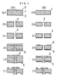
- the pierced hole 3 to be used as through hole is formed in the board with a specified size in the processing stages of (a) and (b), then, the copper film 4 is formed over the entire surface of the board, including the surface of the through hole 3, by electroless plating, in the process (c). Thereafter, by taking the respective processing steps of the formation of the plating resist film 6 ((d) of Figure 1 (B)), the formation of the plated copper for the wiring section by electroplating ((a) of Figure 1 (B)), and the etching ((f) of Figure 1 (B)), the circuit board having the through holes with the desired wiring pattern is obtained.
- the manufacturing method with processing stages shown in (A) of Figure 1 uses the two-side copper-clad laminate as the starting material for the board, therefore, it is advantageous in that the defect as mentioned above can be avoided.
- this two-side copper-clad laminate generally has the characteristic of effecting firm adhesion between the board and the copper foil, it is free of problems such as pattern separation. Also, it has the other merit that low price, low cost circuit boards can be manufactured.
- this manufacturing method uses a wiring pattern designed to have a double layer structure, there are the following disadvantages accompanying it. That is, first, a long time is required for etching, thereby making it unworkable to obtain fine line, high precision patterning. Second, the waste in amount of copper used becomes large, resulting in a hindrance imposed on cost reduction.
- the process is proceeded to the electroless plating of the through hole 3.
- the plating solution used in this process is obtained, for example, by using copper sulfate as metallic salt, while using formalin as reducing agent.
- a several micron thick copper film 4 is obtained as the substrate metal.
- surface activation is performed as a pretreatment, by using a palladium solution, etc.
- the electroplating process is started, by using the conductive ink 7 printed in the process (e), as the electrode at one end.
- the amount of the copper used that affects greatly on the manufacturing cost can be minimised, and also the etching time can be reduced. Therefore, high precision and high density patterning can be implemented.
- the power consumption can be substantially cut down, thereby contributing also in terms of the energy economisation.
Landscapes
- Engineering & Computer Science (AREA)
- Manufacturing & Machinery (AREA)
- Microelectronics & Electronic Packaging (AREA)
- Printing Elements For Providing Electric Connections Between Printed Circuits (AREA)
Claims (5)
Applications Claiming Priority (2)
| Application Number | Priority Date | Filing Date | Title |
|---|---|---|---|
| JP116566/81 | 1981-07-25 | ||
| JP56116566A JPS5932915B2 (ja) | 1981-07-25 | 1981-07-25 | スル−ホ−ルを有する配線基板製造方法 |
Publications (3)
| Publication Number | Publication Date |
|---|---|
| EP0071375A2 EP0071375A2 (de) | 1983-02-09 |
| EP0071375A3 EP0071375A3 (en) | 1983-08-03 |
| EP0071375B1 true EP0071375B1 (de) | 1986-04-23 |
Family
ID=14690274
Family Applications (1)
| Application Number | Title | Priority Date | Filing Date |
|---|---|---|---|
| EP82303763A Expired EP0071375B1 (de) | 1981-07-25 | 1982-07-16 | Verfahren zur Herstellung einer Schaltungsplatte mit einem Durchführungsloch |
Country Status (4)
| Country | Link |
|---|---|
| US (1) | US4389278A (de) |
| EP (1) | EP0071375B1 (de) |
| JP (1) | JPS5932915B2 (de) |
| DE (1) | DE3270751D1 (de) |
Families Citing this family (34)
| Publication number | Priority date | Publication date | Assignee | Title |
|---|---|---|---|---|
| US4633035A (en) * | 1982-07-12 | 1986-12-30 | Rogers Corporation | Microwave circuit boards |
| US4525247A (en) * | 1982-07-12 | 1985-06-25 | Rogers Corporation | Microwave circuit boards and method of manufacture thereof |
| JPS60235014A (ja) * | 1984-05-07 | 1985-11-21 | Nippon Pneumatic Kogyo Kk | 水準器 |
| DE3427015A1 (de) * | 1984-07-21 | 1986-01-30 | Nippon Mektron, Ltd., Tokio/Tokyo | Verfahren zur herstellung von durchkontaktierungen in gedruckten schaltungen |
| JPS6190492A (ja) * | 1984-10-11 | 1986-05-08 | 四国化成工業株式会社 | 銅スル−ホ−ルプリント配線板の製造方法 |
| FR2587575B1 (fr) * | 1985-09-18 | 1987-12-24 | Eat Etude Assistance Tech | Procede pour la fabrication de supports de circuits electriques |
| US4854040A (en) * | 1987-04-03 | 1989-08-08 | Poly Circuits, Inc. | Method of making multilayer pc board using polymer thick films |
| US4775573A (en) * | 1987-04-03 | 1988-10-04 | West-Tronics, Inc. | Multilayer PC board using polymer thick films |
| USRE35064E (en) * | 1988-08-01 | 1995-10-17 | Circuit Components, Incorporated | Multilayer printed wiring board |
| US5155655A (en) * | 1989-08-23 | 1992-10-13 | Zycon Corporation | Capacitor laminate for use in capacitive printed circuit boards and methods of manufacture |
| US5079069A (en) * | 1989-08-23 | 1992-01-07 | Zycon Corporation | Capacitor laminate for use in capacitive printed circuit boards and methods of manufacture |
| JP2636537B2 (ja) * | 1991-04-08 | 1997-07-30 | 日本電気株式会社 | プリント配線板の製造方法 |
| US5261153A (en) * | 1992-04-06 | 1993-11-16 | Zycon Corporation | In situ method for forming a capacitive PCB |
| US5800575A (en) * | 1992-04-06 | 1998-09-01 | Zycon Corporation | In situ method of forming a bypass capacitor element internally within a capacitive PCB |
| EP0584386A1 (de) * | 1992-08-26 | 1994-03-02 | International Business Machines Corporation | Leiterplatte und Herstellungsverfahren für Leiterplatten |
| US6303181B1 (en) | 1993-05-17 | 2001-10-16 | Electrochemicals Inc. | Direct metallization process employing a cationic conditioner and a binder |
| US5725807A (en) * | 1993-05-17 | 1998-03-10 | Electrochemicals Inc. | Carbon containing composition for electroplating |
| US5476580A (en) * | 1993-05-17 | 1995-12-19 | Electrochemicals Inc. | Processes for preparing a non-conductive substrate for electroplating |
| US6710259B2 (en) | 1993-05-17 | 2004-03-23 | Electrochemicals, Inc. | Printed wiring boards and methods for making them |
| US6171468B1 (en) | 1993-05-17 | 2001-01-09 | Electrochemicals Inc. | Direct metallization process |
| US5690805A (en) * | 1993-05-17 | 1997-11-25 | Electrochemicals Inc. | Direct metallization process |
| GB9606497D0 (en) * | 1996-03-27 | 1996-06-05 | Coates Brothers Plc | Production of electrical circuit boards |
| ES2167256B1 (es) * | 2000-07-19 | 2003-10-16 | Lear Automotive Eeds Spain | Procedimiento de interconexion de pistas electroconductoras en circuitos impresos de doble cara para aplicaciones de potencia. |
| TW511423B (en) * | 2001-09-25 | 2002-11-21 | Benq Corp | Soft circuit board for recognition and the manufacturing method thereof |
| WO2012117533A1 (ja) * | 2011-03-02 | 2012-09-07 | 株式会社メイコー | 貫通穴めっき方法及びこれを用いて製造された基板 |
| TWI504322B (zh) * | 2012-03-29 | 2015-10-11 | Taiwan Green Point Entpr Co | 雙面電路板及其製備方法 |
| CN102638947B (zh) * | 2012-04-24 | 2014-12-31 | 杭州新三联电子有限公司 | 银浆跨线印制线路板生产工艺 |
| US20140123487A1 (en) * | 2012-11-08 | 2014-05-08 | Boardtek Electronics Corporation | Printed circuit board manufacturing method |
| US20140124124A1 (en) * | 2012-11-08 | 2014-05-08 | Boardtek Electronics Corporation | Printed circuit board manufacturing method |
| JP5624699B1 (ja) * | 2012-12-21 | 2014-11-12 | パナソニック株式会社 | 電子部品パッケージおよびその製造方法 |
| CN104105361B (zh) * | 2014-05-07 | 2018-08-31 | 深圳市环基实业有限公司 | 一种电路板选择性电镀导电孔的方法 |
| CN105568333B (zh) * | 2015-12-31 | 2018-10-16 | 中国电子科技集团公司第十八研究所 | 一种铜导电翅片局部镀银装置 |
| KR102135031B1 (ko) * | 2018-09-27 | 2020-07-17 | 성균관대학교산학협력단 | 전기 화학적 마이그레이션 방지 첨가제 및 이를 이용한 전기 화학적 마이그레이션을 방지하는 방법 |
| CN109475044B (zh) * | 2018-12-07 | 2021-05-18 | 常熟东南相互电子有限公司 | 采用uv激光钻孔直接电镀制作fpc内层的方法 |
Family Cites Families (7)
| Publication number | Priority date | Publication date | Assignee | Title |
|---|---|---|---|---|
| US3306830A (en) * | 1963-06-13 | 1967-02-28 | Bell Telephone Labor Inc | Printed circuit boards and their fabrication |
| GB1174043A (en) * | 1966-03-01 | 1969-12-10 | British Aircraft Corp Ltd | Improvements relating to the manufacture of Printed Circuits |
| US3799802A (en) * | 1966-06-28 | 1974-03-26 | F Schneble | Plated through hole printed circuit boards |
| FR1534709A (fr) * | 1967-01-20 | 1968-08-02 | Philips Eclairage Radio | Procédé de fabrication de circuits imprimés à trous métallisés |
| CH475690A (fr) * | 1967-07-14 | 1969-07-15 | Jaquet Henri | Procédé pour la fabrication de circuits imprimés et circuit imprimé obtenu par ce procédé |
| US4135988A (en) * | 1978-01-30 | 1979-01-23 | General Dynamics Corporation | One hundred percent pattern plating of plated through-hole circuit boards |
| US4211603A (en) * | 1978-05-01 | 1980-07-08 | Tektronix, Inc. | Multilayer circuit board construction and method |
-
1981
- 1981-07-25 JP JP56116566A patent/JPS5932915B2/ja not_active Expired
-
1982
- 1982-07-02 US US06/394,620 patent/US4389278A/en not_active Expired - Lifetime
- 1982-07-16 DE DE8282303763T patent/DE3270751D1/de not_active Expired
- 1982-07-16 EP EP82303763A patent/EP0071375B1/de not_active Expired
Also Published As
| Publication number | Publication date |
|---|---|
| EP0071375A2 (de) | 1983-02-09 |
| EP0071375A3 (en) | 1983-08-03 |
| US4389278A (en) | 1983-06-21 |
| JPS5932915B2 (ja) | 1984-08-11 |
| DE3270751D1 (en) | 1986-05-28 |
| JPS5818996A (ja) | 1983-02-03 |
Similar Documents
| Publication | Publication Date | Title |
|---|---|---|
| US4389278A (en) | Method for manufacturing circuit board with through hole | |
| EP0226620B1 (de) | Verfahren zur herstellung von gedruckten schaltungsplatten | |
| US5733466A (en) | Electrolytic method of depositing gold connectors on a printed circuit board | |
| KR100427794B1 (ko) | 다층 배선 기판의 제조 방법 | |
| US20050241954A1 (en) | Electrolytic gold plating method of printed circuit board | |
| CN113056116A (zh) | 一种镀孔铜的方法及电路板的加工方法 | |
| GB2086139A (en) | Method of producing printed circuit boards with holes having metallized walls | |
| US4622106A (en) | Methods for producing printed circuits | |
| EP0784914B1 (de) | Verfahren zur herstellung einer leiterplatte | |
| US7240431B2 (en) | Method for producing multilayer printed wiring board, multilayer printed wiring board, and electronic device | |
| WO1998009485A1 (en) | Pattern plating method for fabricating printed circuit boards | |
| US6527963B1 (en) | Method of manufacturing multilayer wiring boards | |
| US5922517A (en) | Method of preparing a substrate surface for conformal plating | |
| JP2001111201A (ja) | 配線板の製造方法およびそれを用いて製造された配線板 | |
| EP0476065B1 (de) | Verfahren zur erhöhung des isolationswiderstandes von leiterplatten | |
| KR20150080565A (ko) | 전기 부품 및 전기 부품을 제조하는 방법 | |
| JPH0243356B2 (de) | ||
| US7451540B2 (en) | Method for fabricating a printed circuit board | |
| JPS6339119B2 (de) | ||
| JPH05259614A (ja) | プリント配線板の樹脂埋め法 | |
| KR100525224B1 (ko) | PCB 상에 Cu, Ni 및 Au를 단일 공정으로도금하는 방법 | |
| JPH08255870A (ja) | 電子部品実装板及びその製造方法 | |
| EP0090900A1 (de) | Verfahren zur Herstellung gedruckter Schaltungsplatten und durch dieses Verfahren hergestellte gedruckte Schaltungsplatten | |
| JPH10135604A (ja) | 105乃至400ミクロン膜厚並びに17乃至105ミクロン膜厚のハイブリットプリント回路の製造方法 | |
| JP3439779B2 (ja) | プリント配線板の製造方法及びプリント配線板 |
Legal Events
| Date | Code | Title | Description |
|---|---|---|---|
| PUAI | Public reference made under article 153(3) epc to a published international application that has entered the european phase |
Free format text: ORIGINAL CODE: 0009012 |
|
| AK | Designated contracting states |
Designated state(s): DE FR GB |
|
| PUAL | Search report despatched |
Free format text: ORIGINAL CODE: 0009013 |
|
| AK | Designated contracting states |
Designated state(s): DE FR GB |
|
| 17P | Request for examination filed |
Effective date: 19840120 |
|
| GRAA | (expected) grant |
Free format text: ORIGINAL CODE: 0009210 |
|
| AK | Designated contracting states |
Kind code of ref document: B1 Designated state(s): DE FR GB |
|
| REF | Corresponds to: |
Ref document number: 3270751 Country of ref document: DE Date of ref document: 19860528 |
|
| ET | Fr: translation filed | ||
| PLBI | Opposition filed |
Free format text: ORIGINAL CODE: 0009260 |
|
| 26 | Opposition filed |
Opponent name: SIEMENS AKTIENGESELLSCHAFT, BERLIN UND MUENCHEN Effective date: 19870116 |
|
| RDAG | Patent revoked |
Free format text: ORIGINAL CODE: 0009271 |
|
| STAA | Information on the status of an ep patent application or granted ep patent |
Free format text: STATUS: PATENT REVOKED |
|
| GBPR | Gb: patent revoked under art. 102 of the ep convention designating the uk as contracting state | ||
| 27W | Patent revoked |
Effective date: 19880118 |