EP0071912A1 - Appareil de mesure - Google Patents
Appareil de mesure Download PDFInfo
- Publication number
- EP0071912A1 EP0071912A1 EP82106917A EP82106917A EP0071912A1 EP 0071912 A1 EP0071912 A1 EP 0071912A1 EP 82106917 A EP82106917 A EP 82106917A EP 82106917 A EP82106917 A EP 82106917A EP 0071912 A1 EP0071912 A1 EP 0071912A1
- Authority
- EP
- European Patent Office
- Prior art keywords
- measurement apparatus
- circuit
- optical
- physical quantity
- upper processor
- Prior art date
- Legal status (The legal status is an assumption and is not a legal conclusion. Google has not performed a legal analysis and makes no representation as to the accuracy of the status listed.)
- Granted
Links
Images







Classifications
-
- G—PHYSICS
- G06—COMPUTING OR CALCULATING; COUNTING
- G06F—ELECTRIC DIGITAL DATA PROCESSING
- G06F11/00—Error detection; Error correction; Monitoring
- G06F11/07—Responding to the occurrence of a fault, e.g. fault tolerance
- G06F11/16—Error detection or correction of the data by redundancy in hardware
- G06F11/1608—Error detection by comparing the output signals of redundant hardware
- G06F11/1625—Error detection by comparing the output signals of redundant hardware in communications, e.g. transmission, interfaces
-
- G—PHYSICS
- G01—MEASURING; TESTING
- G01D—MEASURING NOT SPECIALLY ADAPTED FOR A SPECIFIC VARIABLE; ARRANGEMENTS FOR MEASURING TWO OR MORE VARIABLES NOT COVERED IN A SINGLE OTHER SUBCLASS; TARIFF METERING APPARATUS; MEASURING OR TESTING NOT OTHERWISE PROVIDED FOR
- G01D5/00—Mechanical means for transferring the output of a sensing member; Means for converting the output of a sensing member to another variable where the form or nature of the sensing member does not constrain the means for converting; Transducers not specially adapted for a specific variable
- G01D5/12—Mechanical means for transferring the output of a sensing member; Means for converting the output of a sensing member to another variable where the form or nature of the sensing member does not constrain the means for converting; Transducers not specially adapted for a specific variable using electric or magnetic means
- G01D5/244—Mechanical means for transferring the output of a sensing member; Means for converting the output of a sensing member to another variable where the form or nature of the sensing member does not constrain the means for converting; Transducers not specially adapted for a specific variable using electric or magnetic means influencing characteristics of pulses or pulse trains; generating pulses or pulse trains
- G01D5/248—Mechanical means for transferring the output of a sensing member; Means for converting the output of a sensing member to another variable where the form or nature of the sensing member does not constrain the means for converting; Transducers not specially adapted for a specific variable using electric or magnetic means influencing characteristics of pulses or pulse trains; generating pulses or pulse trains by varying pulse repetition frequency
-
- G—PHYSICS
- G01—MEASURING; TESTING
- G01L—MEASURING FORCE, STRESS, TORQUE, WORK, MECHANICAL POWER, MECHANICAL EFFICIENCY, OR FLUID PRESSURE
- G01L9/00—Measuring steady of quasi-steady pressure of fluid or fluent solid material by electric or magnetic pressure-sensitive elements; Transmitting or indicating the displacement of mechanical pressure-sensitive elements, used to measure the steady or quasi-steady pressure of a fluid or fluent solid material, by electric or magnetic means
- G01L9/12—Measuring steady of quasi-steady pressure of fluid or fluent solid material by electric or magnetic pressure-sensitive elements; Transmitting or indicating the displacement of mechanical pressure-sensitive elements, used to measure the steady or quasi-steady pressure of a fluid or fluent solid material, by electric or magnetic means by making use of variations in capacitance, i.e. electric circuits therefor
-
- G—PHYSICS
- G01—MEASURING; TESTING
- G01R—MEASURING ELECTRIC VARIABLES; MEASURING MAGNETIC VARIABLES
- G01R19/00—Arrangements for measuring currents or voltages or for indicating presence or sign thereof
- G01R19/25—Arrangements for measuring currents or voltages or for indicating presence or sign thereof using digital measurement techniques
- G01R19/252—Arrangements for measuring currents or voltages or for indicating presence or sign thereof using digital measurement techniques using analogue/digital converters of the type with conversion of voltage or current into frequency and measuring of this frequency
-
- G—PHYSICS
- G01—MEASURING; TESTING
- G01R—MEASURING ELECTRIC VARIABLES; MEASURING MAGNETIC VARIABLES
- G01R19/00—Arrangements for measuring currents or voltages or for indicating presence or sign thereof
- G01R19/25—Arrangements for measuring currents or voltages or for indicating presence or sign thereof using digital measurement techniques
- G01R19/255—Arrangements for measuring currents or voltages or for indicating presence or sign thereof using digital measurement techniques using analogue/digital converters of the type with counting of pulses during a period of time proportional to voltage or current, delivered by a pulse generator with fixed frequency
-
- G—PHYSICS
- G06—COMPUTING OR CALCULATING; COUNTING
- G06F—ELECTRIC DIGITAL DATA PROCESSING
- G06F11/00—Error detection; Error correction; Monitoring
- G06F11/07—Responding to the occurrence of a fault, e.g. fault tolerance
- G06F11/16—Error detection or correction of the data by redundancy in hardware
- G06F11/1608—Error detection by comparing the output signals of redundant hardware
-
- H—ELECTRICITY
- H04—ELECTRIC COMMUNICATION TECHNIQUE
- H04B—TRANSMISSION
- H04B10/00—Transmission systems employing electromagnetic waves other than radio-waves, e.g. infrared, visible or ultraviolet light, or employing corpuscular radiation, e.g. quantum communication
- H04B10/50—Transmitters
- H04B10/516—Details of coding or modulation
- H04B10/524—Pulse modulation
-
- H—ELECTRICITY
- H04—ELECTRIC COMMUNICATION TECHNIQUE
- H04B—TRANSMISSION
- H04B10/00—Transmission systems employing electromagnetic waves other than radio-waves, e.g. infrared, visible or ultraviolet light, or employing corpuscular radiation, e.g. quantum communication
- H04B10/60—Receivers
- H04B10/66—Non-coherent receivers, e.g. using direct detection
- H04B10/69—Electrical arrangements in the receiver
-
- H—ELECTRICITY
- H03—ELECTRONIC CIRCUITRY
- H03M—CODING; DECODING; CODE CONVERSION IN GENERAL
- H03M1/00—Analogue/digital conversion; Digital/analogue conversion
- H03M1/12—Analogue/digital converters
- H03M1/60—Analogue/digital converters with intermediate conversion to frequency of pulses
Definitions
- the present invention relates to a measurement apparatus for converting a physical quantity into a digital quantity and for effecting predetermined arithmetic operations on the digital quantity to measure the physical quantity.
- the present invention also relates to a measurement apparatus including a measuring unit for measuring a physical quantity in the above manner, and a transducer or transmitter unit for converting a measured output from the measuring unit into a desired signal and for delivering such a signal.
- a physical change such as a frequency, voltage, electrical resistance, or electrostatic capacity change.
- Many measurement apparatus for effecting such methods have had limitations on measuring accuracy, for example, since a detected output is subjected to analog signal processing before a final output signal is obtained.
- One known transducer for converting a physical quantity into a frequency is a vortex-shedding flowmeter utilizing a von Kármán vortex stream pattern.
- Fig. 1 is illustrative of the principles of such a vortex-shedding flowmeter, the figure being a schematic plan view showing a column-shaped vortex-shedding body OB placed in a fluid flow FL.
- vortices BU are alternately generated downstream of the vortex--shedding body OB one on each side thereof to produce alternate pressure differences on both sides of the vortex-shedding body OB such that the pressure on the side where a vortex is generated is lower than that on the side where no vortex is formed.
- Such a pressure difference is conveyed via an opening or pressure transmission port (not shown) into a vibratory chamber in the vortex-shedding body OB or outside thereof for -vibrating a vibratory plate in the vibratory chamber.
- the number of vortices or the frequency F of generation of vortices which are alternately generated on the sides of the vortex-shedding body can be expressed as: where V is the rate of fluid flow, D is the diameter of the vortex-shedding body, and k is a constant.
- the flow rate or the volume of the fluid as it flows can be derived from the frequency F thus calculated.
- a signal indicative of such a frequency has heretofore been converted into a voltage signal by a frequency-to-voltage (F/V) converter, and the voltage signal has then been converted into a current signal ranging from 4 to 20 mA to thereby effect measurements.
- F/V frequency-to-voltage
- the known measurement apparatus rely on analog circuits and thus are susceptible to measurement errors and have limited measuring accuracy.
- thermocouples or thermoresistances such as a thermistor for temperature measurement have been widely used as elements for converting a physical quantity into a voltage or resistance for detection of the physical quantity. It has been general practice to use an operational amplifier or the like to amplify a thermoelectromotive force generated by the thermocouple or a voltage drop across the thermoresistance, and derive a resistance from an output from the operational amplifier. Such a measurement apparatus is also composed of an analog circuit and thus tends to cause measurement errors, resulting in low measuring accuracy.
- the thermocouple or thermoresistance has a non-linear temperature vs. thermoelectromotive force or temperature vs. resistance characteristic, so that the measurement apparatus needs additional means for linearizing such a non-linear characteristic.
- Transducers for converting a physical quantity into a corresponding capacitance include a differential- pressure or pressure sensor comprising a diaphragm which is displaceable under a differential pressure or a pressure, and a movable electrode such as a capacitor attached to the diaphragm.
- a differential- pressure or pressure sensor comprising a diaphragm which is displaceable under a differential pressure or a pressure, and a movable electrode such as a capacitor attached to the diaphragm.
- a movable electrode EL V is disposed between two fixed electrodes EL F' the movable electrode EL being movable laterally in the directions of the arrow R in response to a change in a physical quantity such as a pressure or a mechanical quantity.
- the displacement ⁇ d can be derived from the capacitance ratio (CA 1 - CA 2 )/(CA 1 + CA 2 ).
- the ratio of CA 1 - CA 2 to CA 2 is given by:
- the displacement ⁇ d can be detected as a change in the electrostatic capacity.
- the measurement apparatus according to the invention is suitable for use in applications in which a pulse signal with a frequency dependent on a physical quantity is obtained directly.
- a measurement apparatus according to the invention and suitable for such uses in which a physical quantity is first detected as a voltage, resistance, or capacitance signal with a magnitude corresponding to the physical quantity is defined in claims 2 through 4.
- the measurement apparatus also needs to be capable of easy zero and spanning adjustment. To meet such a requirement, the measurement apparatus may be constructed as described in claim 5.
- the measurement apparatus as described in the preamble of claim 1 may be used in a measurement apparatus system in combination with means having an electric-to-optical transducer for converting a result of measurement into optical information and delivering such optical information to an upper processor.
- Such a combination has heretofore suffered from the problems as described above.
- Another object of the present invention is to provide a measurement apparatus as described in the preamble of claim 6 which will eliminate the foregoing shortcomings.
- the measurement apparatus can meet the following requirements. First, transmission on a time-sharing multiplex basis should be effected between a single central processing unit and a plurality of measurement apparatus to thereby reduce the cost of a transmission path. Secondly, the measurement apparatus should operate only when necessary to reduce the electric power consumption of the apparatus. The third requirement is that optical parts in an optical transmission circuit be pinned for their failures.According to the fourth requirement, light-emitting elements in the optical transmission circuit should be prevented from being energized accidentally. The fifth requirement is that when the light-emitting and light-receiving elements in the central processing unit and the measurement apparatus, and the transmission path suffer from any trouble, the position at which the trouble is caused, should be detected. The above requirements may easily be met by the measurement apparatus as described in claims 7 through 11.
- the measurement apparatus as described in the preamble of claim 1 can be combined with means for converting a result of measurement into a current signal and delivering such a current signal.
- the combination has heretofore suffered from the above-mentioned disadvantages.
- Still another object of the present invention is to provide a novel measurement apparatus as described in the preamble of claim 12 which will obviate the foregoing disadvantages.
- a measurement apparatus is provided to convert into a digital signal a pulse signal having a frequency dependent on a physical quantity and generated directly by a suitable means, and for effecting predetermined arithmetic operations on the digital quantity to thereby measure the physical quantity.
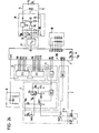
- a measurement apparatus will be described with reference to a block diagram of FIG. 3 and a circuit diagram cf FIG. 4.
- the measurement apparatus comprises a frequency detector 1, an amplifier 2, a counter 4, a timer 5, a reference clock generator circuit 6, a. digital processor 7 such as a microprocessor (hereinafter .referred to as " ⁇ -COM processing circuit"), a battery power supply circuit 9, and a keybord 10.
- ⁇ -COM processing circuit a microprocessor
- the frequency detector 1 may comprise, for example, a frequency detecting device utilizing a von Karman vortex stream pattern.
- the amplifier 2 may comprise an amplifier for amplifying a frequency signal as detected by the detector 1.
- the timer 5 is composed of two-stage counters CT2, CT3 for starting the counting of the clock pulses of a clock signal generated by the reference clock generator circuit 6 when a reset signal P03 from the ⁇ -COM processing circuit 7 is released, and for stopping the counting operation in response to a count-up signal supplied by the counter 4 (CT1).
- CT1 count-up signal supplied by the counter 4
- the w-COM processing circuit 7 is powered by the battery power supply circuit 9 and is driven by the clock signal from the reference clock generator circuit 6 to effect various arithmetic operations and control operations.
- the ⁇ -COM processing circuit 7 When no measurement is effected, for example, the ⁇ -COM processing circuit 7 is responsive to the reset signal P03 to reset the counter 4 and the timer 5. Conversely, when a measurement is to be carried out, the ⁇ -COM processing circuit 7 releases the reset signal P03 to enable the counter 4 and the timer 5 to start their counting operations. The ⁇ -COM processing circuit 7 then receives the count-up signal from the counter 4 as an interrupt signal IRQ, reads the count from the timer 5 through terminals PIO - PI15, and effects predetermined arithmetic operations on read information to thereby measure a physical quantity.
- IRQ interrupt signal
- the keyboard 10 Connected to the ⁇ -COM processing circuit 7 are the keyboard 10 to control zero point and spanning adjustment-to prevent measuring errors, an optical transmission circuit 8 having a light-emitting element LED and a light-receiving element PD for optically transmitting information to or receiving information from an upper processor or computer (not shown) in a control room, a standby mode circuit 12 for intermittently energizing the reference clock generator circuit 6 or the ⁇ -COM processing circuit 7 to save electric power, and a detector circuit 11 for detecting accidental energization (continued energization) of the light-emitting element LED in the optical transmission circuit 8.
- the battery power supply circuit 9 also serves to supply electric power to various parts shown in FIG. 4.
- timer 5 starts counting clock pulses supplied from the reference clock generator circuit 6.
- the counter 4 starts counting a frequency signal as detected by detector 1 and amplified by amplifier 2.
- counter 4 counts a predetermined number (N) , it supplies a count-up signal to the timer 5 to stop counting the clock pulses therein, and at the same time supplies such a count-up signal to the ⁇ -COM processing circuit 7 as the interrupt signal IRQ to instruct the ⁇ -COM processing circuit 7 that the counter 4 has completed its counting operation.
- the ⁇ -COM processing circuit 7 In response to receiving the interrupt signal IRQ, the ⁇ -COM processing circuit 7 reads a count (T) from the timer 5 through the terminals PIO - PI15, effects predetermined arithmetic operations on the received count for thereby measuring a physical quantity which has been detected as being converted into the frequency signal.
- Counting the frequency signal N times in the counter 4 serves to increase resolution of the counters CT2, CT3, and the number N may be selected depending on the frequency of the output pulses from the reference clock generator circuit 6.
- the frequency F can thus be determined by measuring the number of clock pulses which have been counted by the timer 5 before the counter 4 counts the number N, or by measuring the time T required by the timer 5 to count the clock pulses.
- the frequency F can be given by the following equation:
- a measurement apparatus will be described with reference to a block diagram of FIG. 5, a circuit diagram of FIG. 6, and a.waveform diagram of FIG. 7.
- the measurement apparatus finds use in applications in which a physical quantity is first detected as a voltage signal with a magnitude corresponding to the physical quantity.
- the measurement apparatus includes a voltage detector 1, a selector circuit 2 for the detector 1, a frequency converter circuit 3, a counter 4, a timer 5, a reference clock generator circuit 6, a digital processing circuit 7 such as a microprocessor (hereinafter referred to as " ⁇ -COM processing circuit"), an optical transmission circuit 8, a battery power supply circuit 9, and a keyboard 10.
- ⁇ -COM processing circuit a microprocessor
- rIG. 6 shows the voltage detector 1, the detector selector circuit 2, and the frequency converter circuit 3, with the other parts 4 - 12, being the same as shown in FIG. 4.
- the ⁇ -COM processing circuit 7 is shown to indicate additional terminals
- the detector 1 may comprise a thermocouple, for example, and the selector circuit 2 may comprise a switch SW2 (such as a complementary MOS analog switch or relay) for switching conditions of the detector 1.
- the frequency converter circuit 3 is composed of a capacitor C which is chargeable by a constant current flowing from a constant current source CO an operational amplifier OP2 for comparing a voltage Eb to charge the capacitor C and a detected voltage Ea as amplified by an operational amplifier OP1 and for producing an output when the charging voltage Eb is equal to or greater than the detected voltage Ea, a D-type flip-flop Q1 which can be set by the output from the operational amplifier OP2 at a predetermined level (threshold level) and can be reset after expiration of a predetermined interval determined by a time constant (the product of a resistance Rf and a capacitance Cf), and a switch SW1 (switches SW11 , SW12) for actuating the charging and discharging of the capacitors C and Cf.
- flip-flop Q1 Where an ordinary D-type flip-flop is used for the flip-flop Q1, it is necessary to provide a special circuit such as a Schmitt trigger in front of the flip-flop to determine the threshold level. Such an additional circuit may, however, be dispensed with if a CMOS flip-flop is employed, with its switching voltage being used as the threshold voltage. This applies as well for flip-flops Q1 as shown in FIGS. 8, 12 and 24.
- the switch SW1 is of the same construction as that of the switch SW2.
- the ⁇ -COM arithmetic circuit 7 supplies mode selection signals P01, P02 to the switch SW2 in the selector circuit 2 for selection between a measurement mode (hereinafter referred to as "zero measurement mode") in which no detected voltage E 1 is applied, and a detected voltage E 1 measurement mode (hereinafter referred to as “E 1 measurement mode").
- a measurement mode hereinafter referred to as "zero measurement mode”
- E 1 measurement mode a detected voltage E 1 measurement mode
- no mode selection signal P01, P02 is delivered from the n-COM processing circuit 7, and the counter 4 (CT1) and timer 5 remain reset by a reset signal P03.
- CT1 counter 4
- timer 5 remain reset by a reset signal P03.
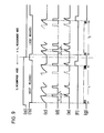
- a zero measurement mode signal as shown at (a) in FIG. 7 is supplied to release the reset signal as shown at (b) in FIG. 7, the capacitor C is charged as shown by Eb at (c) in FIG. 7 by a constant current (I) flowing from the constant-current generating circuit CO.
- the switch SW2 is moved to a position opposite the position shown in FIG. 6, so that no measured voltage El is applied.
- K1K2VDD is expressed as Ea
- the charging voltage for the capacitor C is Eb
- the operational amplifier OP2 compares these voltages Ea, Eb.
- Eb ⁇ Ea the operational amplifier OP2 produces an output to set the flip-flop Q1.
- the relationship between the voltages Ea, Eb is shown at (c) in FIG. 7.
- the flip-flop Q1 When the flip-flop Q1 is set, the output thereof is applied to the counter 4 (CT1) and switch SW1. As a result, the switch SW12 is opened to complete a charging circuit composed of resistor Rf and capacitor Cf. At this time, the switch SW11 will be shifted to a position opposite to that shown in FIG. 6 for allowing the capacitor C to be discharged.
- the charging voltage for the capacitor Cf reaches a predetermined level after a time interval t c as illustrated at (e) in FIG. 7, the flip-flop Q1 is cleared, and consequently it produces an output pulse having the width (t c ) as shown at (d) in FIG. 7.
- the analog switch SW1 When the flip-flop Q1 is reset, the analog switch SW1 is turned off to return the switches SW11, SW12 to the illustrated positions in FIG. 6, whereupon the switch SW11 makes a charging circuit for the capacitor C and the switch SW12 makes a discharging circuit for the capacitor Cf. Since the time t 1 (shown at (d) in FIG. 7) required for the charging voltage to reach an input measured voltage is proportional to the latter, the flip-flop Q1 generates at its output a pulse signal having a frequency which is proportional to the voltage being measured. The pulse signal is counted by the counter 4, and when the count in the counter 4 reaches a predetermined value, the counter 4 produces a count-up output as shown at (f) in FIG.
- the timer 5 has been counting clock pulses supplied from the pulse generator circuit 6 since the release of the reset signal P03. As soon as counting is stopped, the count in the timer 5 is read via the terminals PIO - PI15 by the P -COM processing circuit 7 which has been supplied with the count-up signal from the counter 4.
- the charging and discharging time T 1 for the capacitor C can be measured by counting clock pulses from the reference clock generator circuit 6 before the capacitor C is charged and discharged n times. (To be more precise, only the charging time is measured.) As charging (t 1 ) is effected n times and discharging (t ) is effected (n - 1) times as shown at (d) in FIG. 7, the charging and discharging time T 1 can be determined by the following equation:
- Counting the capacitor chargings for n times results in increased resolution of the time measuring counters CT2, CT3, and the number n may be selected depending on the output frequency of the reference clock generator circuit 6 or the capacitance of the capacitor C.
- the ⁇ -COM processing circuit 7 moves the switch SW2 with the mode selection signals P01, P02 to the E 1 measurement mode and then measures a charging and discharging time T 2 for the capacitor C in the foregoing manner.
- the mode of operation for E 1 measurement is entirely the same as mentioned above, with its time chart being shown at E 1 measurement mode on the right-hand side of FIG. 7. Since a measured voltage E 1 is applied to the input terminal E a of the operational amplifier OP2, a charging time t 2 for the capacitor C can be given as in equation (5) by:
- the charging and discharging time T 2 for the capacitor C can be expressed as in equation (6) by:
- the measured input voltage can thus be derived from the difference between the charging and discharging times T 2 , T 1 for the capacitor C in the E 1 measurement mode and the zero measurement mode.
- the ⁇ -COM processing circuit 7 effects an arithmetic operation to determine such a time difference, and carries out a predetermined conversion to measure the voltage or physical quantity.
- a change in a physical quantity is converted to a voltage change for measurement, and such a voltage change is in turn converted to a frequency signal.
- the frequency signal is then converted into a corresponding digital signal, on which predetermined arithmetic operations are effected to measure the physical quantity.
- the measurement apparatus is therefore advantageous in that it can measure physical quantities with increased accuracy, and can easily perform a variety of compensational arithmetic operations such as for zero point and spanning adjustment, temperature compensation and the like simply by changing programs for the ⁇ -COM processing circuit 7.
- a measurement apparatus is suitable for use in applications in which a physical quantity is first detected as a resistance (electrical resistance) signal with a magnitude corresponding to the physical quantity.
- the measurement apparatus will be described with reference to the block diagram of FIG. 5 (the voltage detector 1 in FIG. 5 is replaced by a resistance detector 1), a circuit diagram of FIG. 8, and a waveform diagram of FIG. 9.
- a modified measurement apparatus will then be described with reference to FIGS. 10 and 11.
- a detector 1 is composed of a measurement resistor R a.nd a standard resistor R C .
- a detector selector circuit 2 comprises a switch SW2 (such as a relay or CMOS analog switch for example) for selecting either resistor R 1 or resistor R c .
- a frequency converter circuit 3 is connected in series with the resistor R or resistor R and includes a switch SW1 (SW11, SW12) for selectively charging or discharging a capacitor C with a current dependent on the resistance of the resistor R 1 or R c , (the capacitor is charged in the illustrated embodiment) and for clearing or resetting a D-type flip-flop Q1.
- the flip-flop Q1 can be set when the charging voltage for the capacitor C exceeds a predetermined voltage level (threshold level) , and reset after expiration of a predetermined period of time which is determined by a time constant (the product of resistance Rf and capacitance Cf).
- the ⁇ -COM processing circuit 7 delivers mode selection signals P01, P02 to the switch SW2 in the selector circuit 2 to select the resistor R 1 measurement mode (R 1 mode) or the resistor R c measurement mode (R c mode).
- the measurement apparatus operates as follows: With reference to FIGS. 8 and 9, under an initial condition, no mode selection signal P01, P02 is given by the ⁇ -COM processing circuit 7.
- the counter4 (CT1) and the timer 5 remain reset by the reset signal P03.
- a resistor R 1 measurement mode signal as shown at (a) in FIG. 9 is supplied to release the reset signal P03 as shown at (b) in FIG. 9, a path is formed from the power supply VDD to the resistor R 1 ,to the switch SW2,to the switch SW11 and to the capacitor C, whereupon the capacitor C is charged in the pattern illustrated at (c) in FIG. 9.
- the flip-flop Q1 When the charging voltage for the capacitor C exceeds a threshold voltage VTH for the flip-flop Q1 after a period of time t 1 , the flip-flop Q1 is set and produces an output via its output terminal Q. The output from the flip-flop Q1 is fed to the counter 4 and the switch SW1. As a result, the switch SW12 is opened to complete a charging circuit composed of the resistor Rf and the capacitor Cf. At this time, the switch SW11 is moved to discharge the capacitor C. When the charging voltage for the capacitor C reaches a predetermined level after a predetermined period of time t as shown at (e) in FIG. 9, the flip-flop Q1 is cleared and produces an output pulse with a width t as illustrated at (d) in FIG. 9.
- the switch SW1 Upon resetting the flip-flop Q1, the switch SW1 is also turned off, and the switch SW12 is returned to the position shown in FIG. 8, whereupon a discharging circuit for the capacitor Cf is closed. Since the period of time t 1 is in proportion to the capacitance of the capacitor C and the resistance of the resistor R 1 , the flip-flop Q1 produces via its output a pulse signal with a frequency which is proportional to the resistance of the resistor R 1 . The pulse signal from the flip-flop Q1 is counted by the counter 4. When the count in counter 4 reaches a predetermined value, the counter 4 produces a count-up output as shown at (f) in FIG. 9 to de-energize the timer 5 to stop it from counting as shown at (g) in FIG. 9.
- the timer 5 has been counting clock pulses supplied from the pulse generator circuit 6 since the release of the reset signal P03.
- the count in the timer 5 is read via the terminals PIO - PI15 by the ⁇ -COM processing circuit 7 which has been supplied with the count-up signal from the counter 4.
- the threshold voltage VTH for the flip-flop Q1 is given as follows:
- the charging time t 1 (as shown at (d) in FIG. 9) for the capacitor C is expressed by: where VDD is the power supply voltage.
- the time period t c can be determined by the following equation: With the resistance of the resistor Rf and the capacitance of the capacitor Cf known, the timer period t c is constant.
- the charging and discharging time T 1 for the capacitor C can be measured based on the output from timer 5 (more precisely, only the charging time is measured).
- charging (t 1 ) is effected n times
- discharging (t c ) is effected (n - 1) times, so that T 1 can be given by:
- n By counting the capacitor chargings n times, the resolution of the time measuring counter (CT2, CT3) is increased.
- the number n may be selected to depend on the output frequency of the reference clock generator circuit 6, the resistance of the resistor R 1 , or the capacitance of the capacitor C. In the illustrated embodiment, n is selected to be 256.
- the ⁇ -COM processing circuit 7 After the charging and discharging time T 1 for the capacitor C has been determined, the ⁇ -COM processing circuit 7 produces the signal P01 or PO2 to shift the switch SW2 for the resistor R c measurement mode, so that a charging and discharging time T 2 for the capacitor C can be measured in a similar manner.
- the mode of operation for R c measurement is entirely the same as described above.
- a charging time t 2 can be expressed by the following equation:
- the charging and discharging time T 2 can be given by:
- the ⁇ -COM arithmetic circuit 7 effects the following arithmetic operations based on the above equations (10), (11):
- the following equation can be used to determine an unknown resistance R 1 .
- the arithmetic operation according to equation (12) is effected to divide variations in the capacitance of the capacitor C, the power supply voltage VDD, or the threshold voltage VTH to thereby remove any influences that the above variations have.
- the switches SW1, SW2 comprise CMOS analog switches, they may pose a problem, since they present resistance when turned on. To avoid this problem, the switches SW1, SW2 may be designed as relay contacts.
- a switch SW2 is moved successively to determine charging and discharging times for the capacitor C which differ with resistances R 1 + 2Rl, 2Rl, and R c .
- charging times with the resistances R 1 + 2Rl, 2RI, and R c are t 1 , t 2 and t3, respectively, and charging and discharging times with the above resistances are T 1 , T 2 and T 3' respectively, these times can be expressed as follows:
- the ⁇ -COM processing circuit 7 implements the arithmetic operation expressed by equation (13) to measure the resistance R 1 .
- F I G. 11A shows a pair of wire strain gauges R 1 , R 2 attached to both sides of an object OB for measuring a pressure F or a displacement ⁇ d imposed on the object OB.
- FIG. 11 g illustrates a circuit arrangement for measuring the resistances R 1 , R 2 .
- the mode of operation of the arrangement of FIG. 11B is the same as that of the arrangement shown in FIG. 8. More specifically, the switch SW2 is shifted to select either the resistor R 1 or R 2 for determining the charging times t 1 , t 2 and the charging and discharging times T 1 , T 2 for the resistors R 1 , R 2 , respectively, and the following arithmetic operation is implemented:
- a change in a physical quantity is converted into a resistance change, which is then converted into a corresponding frequency signal.
- the frequency signal is thereafter converted into a digital signal, on which predetermined arithmetic operations are effected to measure the physical quantity.
- the measurement apparatus can measure physical quantities with increased accuracy, and can perform various compensational arithmetic operations such as zero point and spanning adjustment and temperature compensation simply by changing programs for the ⁇ -COM processing circuit 7.
- the physical quantity is measured by measuring the charging time for the standard capacitor C
- the physical quantity can be determined by measuring the discharging time for the capacitor C in the same manner.
- the capacitor C and the flip-flop Q1 have been described as being shared by both the R 1 and R c measurement modes, separate capacitors and flip-flops may be provided for the R and R measurement modes.
- a measurement apparatus first detects a physical quantity as a capacitance (electrostatic capacity) signal with a magnitude which corresponds to the physical quantity.
- the measurement apparatus will now be described with reference to the block diagram of FIG. 5 (the voltage detector 1 in FIG. 4 is replaced with a capacitance detector 1), a circuit diagram of FIG. 12, and the waveform diagram of FIG. 9 (which is shared by the circuits shown in FIGS. 8 and 12). A modification will also be described with reference to FIG. 13.
- a detector 1 comprises capacitors C1, C 2 and a detector selector circuit 2 comprises a CMOS analog switch SW2 (SW21, SW22) for selecting the capacitor C 1 , C2, a temperature measuring capacitor Cs, or a thermistor Rs.
- a capacitance-to-frequency converter circuit 3 is composed of an analog switch SW1 (SW11, SW12) for effecting charging and discharging of the capacitors C1, C 2 and for clearing or resetting a D-type flip-flop Q1.
- the flip-flop Q1 can be set when the charging voltage for the capacitor C 1 or C 2 exceeds a predetermined voltage level (threshold level), and reset after expiration of a predetermined interval of time determined by a time constant (determined in turn by a resistance Rf and a capacitance Cf).
- the ⁇ -COM processing circuit 7 supplies mode selection signals P01, P02 to the analog switch SW2 in the selector circuit 2 for selecting a capacitance C 1 measurement mode, a capacitance C 2 measurement mode, or a temperature measurement mode (measurement using the resistor Rs and the capacitor Cs).
- the circuits shown in FIGS. 8 and 12 differ from one another only in that the circuit in FIG. 8 relies on a proportional relationship between Rf of the time constant RfCf and the physical quantity to be measured, whereas the circuit in FIG. 12 relies on a proportional relationship between Cf of the time constant RfCf and the physical quantity to be measured.
- the measuring operation of the circuit illustrated in FIG. 12 can thus be understood when reference is made to the foregoing description relating to the operation of the circuit illustrated in FIG. 8.
- the ⁇ -COM processing circuit 7 After the charging and discharging time T 1 for the capacitor C 1 has been determined, the ⁇ -COM processing circuit 7 produces the signal P01 or P02 to shift the switch SW21 for the capacitance C 2 measurement mode in which to measure a charging and discharging time T 2 for the capacitor C 2 .
- the charging and discharging times T 1 , T 2 can be expressed as in equaticns (10), (11) by:
- the ⁇ -COM processing circuit 7 implements the following arithmetic operations based on the above equations:
- the equation (15) is proportional to the displacement, so that the ⁇ -COM processing circuit ? can measure the displacement by implementing the foregoing arithmetic operations.
- the capacitances of the capacitors C 1 , C 2 are varied differentially to measure a physical displacement such as a differential pressure ⁇ P.
- a pressure P should be determined instead of the differential pressure ⁇ P according to the following equation:
- the ⁇ -COM processing circuit 7 shifts the switch SW21 with the signals P01, P02 for the temperature measurement mode.
- a charging and discharging path from the capacitor Cs to switches SW21, SW11, SW22, and to the thermistor R S is closed as with the measurement mode for the capacitors C 1 , C 2 .
- the resistor R is connected in parallel with thermistor Rs, thermistor Rs and resistor R have a relationship of Rs ⁇ R, so that operation will not be influenced by resistor R.
- a charging time t 3 for capacitor Cs is given by:
- a total charging and discharging time T 3 for capacitor Cs is expressed as follows:
- Temperatures can-be measured by storing in advance a relationship between the charging and discharging time T 3 and temperatures in a memory (not shown) of the ⁇ -COM processing circuit 7. Measurenents tend to be affected directly by variations in the voltages VDD and VTH. However, the errors are caused in amounts in compensation only, and hence are negligible.
- the resistor R and the flip-flop Q1 are shared by the detection of the capacitances of the capacitors C 1 , C 2 .
- separate resistors and flip-flops may be provided for respectively detecting the capacitances of the capacitors C1, C 2 .
- the measurement apparatus is composed of a digital circuit so as to be free from influences of noises and temperatures, and hence can measure physical quantities with increased accuracy.
- the apparatus consumes a relatively small amount of electric power. Since influences of temperatures and stray capacities can be compensated for by arithmetic operations, no special compensation circuits are necessary for this purpose. Pressures, instead of differential pressures, can be measured easily simply by changing arithmetic operation% that is, by selecting a suitable program. Thus, the measurement apparatus is of considerable practical advantage.
- the keyboard 10 includes push buttons PB for zero point and spanning adjustment,respectively.
- the ⁇ -COM processing circuit 7 starts performing the above measuring operations under a command from push button PB .
- the result of measurement is then stored in the-memory (not shown) of the u-COM processing circuit 7.
- the foregoing procedure is then repeated after confirming that an input is applied 100%, and the result of arithmetic operations is also stored in the memory. These stored data will be used to compensate for the results of subsequent arithmetic operations.
- the memory in the ⁇ -COM processing circuit 7 should preferably comprise a CMOS RAM (random-access memory) backed up by a battery.
- the measurement apparatus includes the digital arithmetic circuit and the memory for storing the results of arithmetic operations when the input to be measured is 0 and 100% in response to the operation of the push button.
- the storing procedures are free from mutual interference, so that there is no risk of the zero point being shifted during spanning adjustment. Accordingly, adjustment operation is easy and accurate.
- the optical transmission circuit 8 as illustrated in FIGS. 4 and 5 serves to carry out optical transmission of information of the type described, and is constructed as shown in the block indicated by the reference numeral 8 in FIG. 4.
- the optical transmission circuit 8 is composed primarily of a photodiode PD for receiving optical signals transmitted from an upper processor or computer, and a light-emitting diode LED for transmitting optical signals to the upper processor.
- the measurement apparatus is caused to operate only at desired times in response to commands'delivered as optical signals from the upper processor. Results of measurement are transmitted to the upper processor when the light-emitting diode LED in the optical transmission circuit 8 is energized.
- the optical transmission may be performed by a known pulse-width modulation (PWM) or pulse-code modulation (PCM) system, or otherwise simply by delivering optical signals with predetermined frequencies or wavelengths.
- PWM pulse-width modulation
- PCM pulse-code modulation
- information can be transmitted in a multiplex mode. Since the measurement apparatus operates only at required times, it may be powered by a battery poMer supply circuit 9 of relatively small capacity designed to supply electric power to various parts of the measurement apparatus.
- the battery power supply circuit 9 may comprise a lithium cell, an automatically chargeable combination of a solar cell and a nickel-cadmium battery, or a nickel-cadmium battery that can be put into operation when supplied with optical power.
- the measurement apparatus is a digital circuit construction which is free from adverse effects caused by noises or temperatures.
- the measurement apparatus features increased measuring accuracy and a relatively small power requirement.
- Optical transmission of information between the measurement apparatus and the upper processor or computer is not adversely affected by noises or surges, resulting in a higher measuring accuracy.
- the measurement apparatus with the optical transmission system can be safely used in an explosive environment.
- FIG. 14 shows a system arrangement
- FIG. 15 illustrative of forms of information transmitted between the central processing unit and the measurement apparatus
- FIG. 16 which is a timing chart for information transmitting and receiving operations
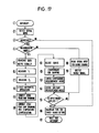
- FIG. 17 which is a flow chart for measuring operations.
- the system includes a central control room CE having therein a central processing unit CPU and a transducer or transmitter unit CO including electric-to-optical and optical-to-electric transducers, a plurality of digital measurement apparatus TR1 - TR (hereinafter referred to as "transmitter”) for measur - ing a variety of physical quantities, a star coupler (commercial name) for mixing and dividing optical information between the central processing unit CPU and the transmitters TR, and optical fibers OFS, OFM.
- the star coupler SC is located in the field for economical reasons so that the optical fibers OFM coupled to the transmitters TR will not be too long.
- FIG. 15 shows forms of information delivered between the transmitters TR and the central processing unit CPU.
- FIG. 15(a) is illustrative of control information CS
- FIG. 15(b) shows a form of information transmitted from the central processing unit CPU to the transmitters TR for setting a measurement range (a condition hereinafter referred to as a "range setting mode")
- FIG. 15(c) illustrates a form of information delivered when measured data are transmitted from a transmitter TR to the central processing unit CPU (a condition called a "measurement mode")
- FIG. 15(d) shows a form of information sent back from a transmitter TR to the central processing unit CPU for confirming that the transmitter has received range setting information from the central processing unit CPU.
- the control information CS is composed of a start bit ST (D 0 ), address informa tionAD (D 1 - D 3 ) indicative of the identification num- ber of each transmitter, mode information MO (D 4 ) indicative of the measurement mode or the range setting mode, auxiliary information AU (D 5 , D,), and a parity bit PA (D 7 ).
- the informa tion as shown in FIG. 15(a) is delivered from the central processing unit CPU to the transmitters TR, and control information CS and measured data DA as shown in FIG. 15(c) are transmitted from an addressed transmitter TR to the central processing unit CPU.
- All of the transmitters TR are put into operation simultaneously in response to the start bit ST, and those transmitters TR which are not addressed will be de-energized after expiration of a predetermined time interval.
- the transmitters TR are supplied with the control information CS as illustrated in FIG. 15(b), and after expiration of a predetermined time period,with zero point information ZE including the start bit ST and spanning information SP, whereupon .
- the transmitters TR deliver the received information as shown in FIG. 15(d) back to the central processing unit CPU to thereby inform the latter that they have properly received the range setting information.
- the transmitters TR1, TRK receive the information CS1, CSK after a predetermined period of time as illustrated in FIG. 16(b).
- the transmitter TR1 then operates as shown in FIG. 16(c).
- the transmitter TRK stops operating a predetermined period of time ⁇ 3 after the information CS1 has been supplied, and starts to operate in response to receiving the information CSK.
- ⁇ 2 a one-cycle period required to call the transmitter of the same address, that is, a period of time required for one transmitter to effect measurement and arithmetic operations, access time intervals for or the order of selection of the trans- mitterscan be freely selected or changed for transmitting information.
- the w-COM processor in the transmitter starts to operate in response to an interrupt signal (start signal) supplied from the upper computer CPU (1), reads an input signal (control information) as shown in FIG. 15 (2), and determines whether the transmitter is addressed or not by the received input signal (3). If it is not addressed, then a predetermined time is maintained (16) and the transmitter enters a mode for awaiting a next interrupt (17), so that the transmitter will not operate in error in response to range setting information for another transmitter. If the transmitter is addressed, the ⁇ -COM processor therein determines if the measurement mode is selected or not (4).
- the u-COM processor reads input data-for changing the range (18), delivers the input data back to the upper computer CPU to confirm that the input data has been received (19), confirms that there is another input signal (15) to prevent erroneous operation due to another such input signal, thereafter maintains a predetermined period of time (16), and enters into an interrupt awaiting mode (17).
- the measurement mode is selected at step (4), the result of previous arithmetic operations is then transmitted serially (5), the charging and discharging time T 1 is measured (6) to effect predetermined arithmetic operations, time T 2 is also measured if necessary (7), and necessary arithmetic operations are performed on the basis of the data of the above measurements (8): Compensation for a zero point and spanning is then effected (9), and similarly, compensation for a zero point and spanning due to temperatures is carried out (10). Thereafter, the w-COM processor adjusts the range (11) based on the range setting information which has already been received from the central processing unit CPU on the panel. If there is any damping, a predetermined arithmetic operation is performed to compensate for such damping (12).
- the temperature is measured (13), the battery voltage is measured (14), another input signal is confirmed (15) to prevent the transmitter from malfunctioning due to such another input signal. Subsequently, a predetermined period of time is inserted (16), and the transmitter enters the interrupt awaiting mode (17).
- the measurement apparatus is a circuit arrangement capable of digital processing for increased measuring accuracy.
- the measurement apparatus or transmitters coupled to an upper processor through optical transmission paths, information on measured data or other data can be transmitted quite reliably over the optical transmission paths without being adversely affected by noises or surges. Since the transmitters are optically coupled to the upper processor by the star coupler, the number and length of optical transmission paths can be reduced, resulting in an economical advantage.
- the system of the present invention is also advantageous in that the failure of one transmitter does not adversely affect other transmitters while in operation, an advantage over systems in which transmitters are continuously coupled with each other.
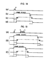
- FIG. 4 and FIGS. 18, 19 are timing charts for signals.
- the measurement apparatus performs predetermined operations under the command from the central processing unit installed in the central control room.
- a command is received by the photodiode PD in the optical transmission circuit 8.
- a transistor TR is switched to become conductive, supplying a signal at a low logic level to an inverter IN.
- the inverter IN applies an inverted signal to an input terminal SI of the ⁇ -COM processing circuit 7 and a terminal CP of a flip-flop FF in the standby mode circuit 12.
- the flip-flop FF is then set, and the u-COM processing circuit 7 is released from the standby condition as illustrated in FIG. 18(b).
- An output from a terminal Q of the flip-flop FF as it is set is delayed for a predetermined period of time (as shown by t in FIG. 18(c))by a delay circuit comprising a resistor R SB and a capacitor C SB .
- the clock generator circuit 6 starts to operate after expiration of such a period of time t as shown in FIG. 18(c).
- the ⁇ -COM processing circuit 7 also starts operating as shown in FIG. 18(d) to perform predetermined arithmetic operations under the command from the central processing unit.
- the ⁇ -COM processing circuit 7 resets the flip-flop FF via a terminal P04 (as shown by the arrow Re in FIG. 18).
- the ⁇ -COM processing circuit 7 enters a standby mode in response to the reception of a reset signal from a terminal Q of the flip-flop FF.
- the clock generator circuit 6 and the w-COM processing circuit 7 do not stop their operation immediately, but are delayed for an interval t before they are inactivated.
- the ⁇ -COM processing circuit 7 is de-energized after it has completed its arithmetic operations and the interval t has been inserted in which the ⁇ -COM processing circuit 7 enters the standby mode.
- the above process deals with intermittent operation of the single measurement apparatus connected to the central processing unit.
- the manner in which a plurality of measurement apparatus connected to the central processing unit are driven intermittently in parallel with one another will be described with reference to FIG. 19.
- the plurality of measurement apparatus are simultaneously started by start information (as shown by a signal ST in FIG. 19(A)) supplied from the central processing unit CPU, whereupon the 4 -COM processing circuits in the measurement apparatus are released from a standby condition, and the clock generator circuits therein start operating after expiration of a predetermined delay time.
- start information as shown by a signal ST in FIG. 19(A)
- the central processing unit CPU whereupon the 4 -COM processing circuits in the measurement apparatus are released from a standby condition, and the clock generator circuits therein start operating after expiration of a predetermined delay time.
- the addressed measurement apparatus enter a standby condition after they have performed predetermined arithmetic operations as shown by arrow H1.
- the measurement apparatus that are not addressed are shifted to a standby condition after expiration of a predetermined interval of time as indicated by arrow H2 in FIG. 19(C).
- the measurement apparatus are controlled by their own ⁇ -COM processing circuits so as not to effect an undesired operation, thus reducing electric power consumption.
- the clock generator circuit and the digital arithmetic circuit in the measurement apparatus which are powered by a battery and consume relatively much electric power, are energized only as required.
- the measurement apparatus can, therefore, be battery-powered and largely reduces its power consumption.
- FIG. 20 A system in which optical parts in an optical transmission circuit can be traced for failure or malfunction will be described with reference to a block diagram of FIG. 20 and a timing chart of FIG. 21.
- the system illustrated in FIG. 20 includes a star coupler SC (commercial name), optical fibers OFS, OFM and a plurality of measurement apparatus or transmitters TR1 - TRn.
- the measurement apparatus TR1 - TRn include electric-to-optical transducers E01 - EOn, optical-to-electric transducers OE1 - OEn, delay circuits DL1 - DLn such as shift registers, monostable multivibrators, or timers for detecting parts failures, and measuring units PM1 - PMn for measuring physical quantities, all respectively.
- the transducers OE1 - OEn, E01 - EOn, and the delay circuits DL1 - DLn constitute transmitting units, respectively.
- a control signal is delivered from an upper computer (not shown) via the star coupler SC to the measurement apparatus, in which the control signal is received by the optical-to-electric transducers OE1 - OEn as shown by FIG. 21(a).
- the delay circuits DL1 - DLn are designed to delay signals for mutually different delay times.
- the control signal is delayed for different times ⁇ A , ⁇ B , ... ⁇ N by the delay circuits, respectively, as shown in FIGS. 21(b) through 21(d), and delayed signals are fed to the electric-to-optical transducers E01 - EOn, respectively, from which the signals are sent back to the upper computer via the star coupler SC.
- the upper computer can ascertain the.
- the failures of optical parts at least in the measurement apparatus can be detected by simple means added to delay a control signal from an upper computer-for predetermined periods of time.
- positions at which optical parts have failed can be traced, and measures can easily be taken against malfunctions which would otherwise be caused by the parts failures.
- the optical transmission circuit 8 includes a transistor TRA in addition to the light-emitting diode LED.
- the accidental LED energization detector circuit 11 comprises a charging circuit composed of a resistor RL and a capacitor CL, _a gate G, and a transistor TRB. Under normal conditions, the transistorsTRA, TRB are energized by a pulse supplied from an output terminal SO of the ⁇ -COM processing circuit 7, completing a circuit for energizing the light-emitting diode LED. If the output from the terminal SO of the ⁇ -COM processing circuit 7 is continuously delivered for some reason, a potential at the point Po gradually increases.
- the circuit for energizing the light-emitting diode LED is broken to thereby de-energize the light-emitting diode LED.
- the potential at the point Po reaches the predetermined level after the certain period of time which is determined by a time constant dependent on the resistor RL and the capacitor CL. Therefore, continued energization of the light-emitting diode LED beyond the predetermined period of time can be detected, and the continuously energized light-emitting diode LED then be de-energized.
- the above detecting operation has no bearing on the operation of the ⁇ -COM processing circuit, which should therefore not be burdened by such detecting operation.
- a means for integrating a current that flows through the light-emitting element for converting measured data into an optical signal and for transmitting the latter When the current as integrated by the means reaches a predetermined level, the light-emitting element is de-energized.
- the measurement apparatus can operate highly reliably.
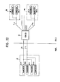
- FIG. 22 is a block diagram of a system according to still another embodiment in which any trouble in the central processing unit, the light-emitting and light-receiving elements in the measurement apparatus, or the transmission paths can be detected positionally.
- the system comprises light-receiving element OE11, OE12, OE21 - OE2n such as photodiodes (PD) , light-emitting elements E011, E012, E021 - E02n such as light-emitting diodes (LED), a central control room or panel CE, a star coupler SC by which two optical transmission paths L1, L 2 are coupled for optical transmission with a plurality of n optical transmission paths L T1 - L Tn , and a plurality of measurement apparatus or transmitters TR 1 - TR n installed in the field.
- PD photodiodes
- E011, E012, E021 - E02n such as light-emitting diodes (LED)
- a central control room or panel CE a star coupler SC by which two optical transmission paths L1, L 2 are coupled for optical transmission with a plurality of n optical transmission paths L T1 - L Tn , and a plurality of measurement apparatus or transmitters TR 1 - TR n
- the measurement apparatus or transmitter TR 1 - TR are coupled by the star coupler SC to the optical trans- misson paths L 1 , L 2 for dividing optical information at the ratio of 2 : n or mixing optical information at the ratio of n : 2, the optical transmission paths L 1 , L 2 being coupled to a central processing unit in the central control room CE.
- the optical transmission paths L 1 , L 2 have a double construction, and the central processing unit in the central control room CE, accordingly has two pairs of light-emitting elements E011, E012 and light-receiving elements OE11, OE12.
- One of the light-emitting elements E011, E012 in the central control room CE is selected to transmit desired information.
- the information is supplied over one of the optical transmission paths L 1 , L 2 to the star coupler SC where the information is divided into n pieces.
- the n pieces of information are delivered respectively over the optical transmission paths L T1 - L Tn and received respectively by the light-receiving elements OE21 - OE2n in the transmitters.
- the transmitters send back certain information via the light-emitting elements E021 - E02n to the central control room CE.
- the central processing unit in the central control room CE can locate a failure, if any, by determining whether the information based on the transmitted command information has been sent back or by checking the content of the received information.
- the light-receiving element OE11 in the central processing unit has failed and no other failure has occured.
- command information is transmitted out of the light-emitting element E011
- responsive information is sent back from the transmitters TR 1 - TR n via the star coupler SC to the optical transmission paths L 1 , L 2 .
- the light-receiving element OE12 receives the returned information, although the light-receiving element OE1 ' 1 cannot receive the returned information because of its failure.
- the light-emitting element E012 is selected to transmit command information, no returned information can be received by the light-receiving element OE11 for the same reason either.
- the light-emitting element.E011 has failed and is selected to deliver command information
- no returned information can be received by either of the light-receiving elements OE11, OE12.
- the light-receiving elements OE11, OE12 can receive such returned information only when the light-emitting element E012 is selected to transmit command information.
- the optical transmission path L 1 has failed, no information can be received by the light-receiving elements OE11, OE12 when command information is transmitted by the light-emitting element E011, but information can be received by the light-receiving element OE12 when the light-emitting element E012 is selected to produce command information.
- a study of the above table indicates that the way in which the light-receiving elementsOE11, OE12 receive information varies with the positions of failure, and hence the central processing unit in the central control room can locate failures by inspecting the pattern of the table. It is inpossible to locate failure positions in the transmission paths L T1 - L Tn and the elements OE21 - 2n, E021 - 2n in the transmitters TR1 - TR n .
- failures can be located in transmitter systems including optical transmission paths and light-emitting and light-receiving elements by checking the contents of returned information.
- the optical transmission paths are of a double circuit construction, and two pairs of light-emitting and light-receiving elements are provided in the central processing unit in the central control room for the double optical transmission paths.
- the entire system therefore, has increased operation reliability, and failures can be located with ease.
- optical digital output Signals are transmitted from the measurement apparatus
- the present invention is applicable to a measurement apparatus for transmitting a current signal indicative of measured data.
- a measurement apparatus will be described with reference to a block diagram of FIG. 23 and a circuit diagram of FIG. 24.
- the measurement apparatus comprises a detector 1, a detector selector circuit 2, a frequency converter circuit 3, a counter 4, a timer 5, a reference clock generator circuit 6, a microprocessor 7 (" ⁇ -COM processing circuit"), a frequency-to-voltage (F/V) converter circuit 13, a voltage-to-current (V/I) converter and transmitter circuit 14, and a keyboard 10.
- the components designated at 1 - 7 and 10 jointly constitute a measuring unit ME and the components designated at 13 and 14 jointly constitute a converter unit CO.
- the F/V converter circuit and the V/I converter and transmitter circuit may be of known construction.
- Data measured as with the foregoing embodiments can be delivered via the frequency-to-voltage (F/V) converter circuit 13 shown in FIGS. 23 and 24 to the voltage-to-current (V/I) converter and transmitter circuit 14 which is capable of producing an output current ranging from 4 to 20 mA, from which the data will be transmitted to a remotely located device (load resistor) on the panel.
- the measuring unit ME (as shown in FIG. 23) has no own power supply and is powered by the V/I converter and transmitter circuit 14 for converting a measured physical quantity in digital form back into a corresponding analog quantity- Such an analog quantity is again converted by the V/I converter circuit 14 into a current in the range of from 4 to 20 mA.
- the F/V converter circuit 13 and the V/I converter and transmitter circuit 14 are provided for ready cooperation with other measurement equipment and devices on the panel. Therefore, the measurement apparatus as shown first converts an analog quantity into a digital quantity, and then converts the digital quantity back into an analog quantity.
- the measuring unit for measuring physical quantities is constructed so as to process digital quantities, and hence improves limited measuring accuracies which conventional analog measuring units have suffered from.
- the measurement apparatus can easily effect various compensational arithmetic operations, and is less influenced by noises or surges with the measuring unit being easily insulated from the voltage-to-current converter circuit.
- the measuring unit may produce an output signal which has been subjected to pulse-width modulation or other output signals in digital form.
- the measuring unit may be insulated from a power supply circuit as well as from the voltage-to-current (V/I) converter circuit to increased advantage.
Landscapes
- Physics & Mathematics (AREA)
- Engineering & Computer Science (AREA)
- General Physics & Mathematics (AREA)
- Theoretical Computer Science (AREA)
- Quality & Reliability (AREA)
- General Engineering & Computer Science (AREA)
- Electromagnetism (AREA)
- Computer Networks & Wireless Communication (AREA)
- Signal Processing (AREA)
- Measurement Of Resistance Or Impedance (AREA)
- Arrangements For Transmission Of Measured Signals (AREA)
- Testing Or Calibration Of Command Recording Devices (AREA)
Priority Applications (1)
| Application Number | Priority Date | Filing Date | Title |
|---|---|---|---|
| DE8484114777T DE3279510D1 (en) | 1981-07-30 | 1982-07-30 | Measurement apparatus |
Applications Claiming Priority (24)
| Application Number | Priority Date | Filing Date | Title |
|---|---|---|---|
| JP56118417A JPS5819998A (ja) | 1981-07-30 | 1981-07-30 | デイジタル式測定装置 |
| JP118415/81 | 1981-07-30 | ||
| JP56118414A JPS5819994A (ja) | 1981-07-30 | 1981-07-30 | 光による測定情報多重伝送方式 |
| JP56118413A JPS5819995A (ja) | 1981-07-30 | 1981-07-30 | 電池内蔵形デイジタル式変位測定装置 |
| JP11841681A JPS5819997A (ja) | 1981-07-30 | 1981-07-30 | 測定装置 |
| JP118416/81 | 1981-07-30 | ||
| JP118413/81 | 1981-07-30 | ||
| JP118417/81 | 1981-07-30 | ||
| JP56118412A JPS5821104A (ja) | 1981-07-30 | 1981-07-30 | 変位測定装置 |
| JP118412/81 | 1981-07-30 | ||
| JP118414/81 | 1981-07-30 | ||
| JP56118415A JPS5819996A (ja) | 1981-07-30 | 1981-07-30 | 測定情報伝送システムにおける故障検出方式 |
| JP120724/81 | 1981-08-03 | ||
| JP120723/81 | 1981-08-03 | ||
| JP56120723A JPS5821935A (ja) | 1981-08-03 | 1981-08-03 | 測定情報多重伝送システムにおける故障位置検出方式 |
| JP56120724A JPS5822966A (ja) | 1981-08-03 | 1981-08-03 | バツテリ内蔵形デイジタル式測定装置 |
| JP12733681A JPS5829097A (ja) | 1981-08-15 | 1981-08-15 | 二線式測定装置 |
| JP127336/81 | 1981-08-15 | ||
| JP132750/81 | 1981-08-26 | ||
| JP13275081A JPS5835697A (ja) | 1981-08-26 | 1981-08-26 | 測定装置 |
| JP56134224A JPS5835415A (ja) | 1981-08-28 | 1981-08-28 | 測定装置 |
| JP134225/81 | 1981-08-28 | ||
| JP13422581A JPS5837795A (ja) | 1981-08-28 | 1981-08-28 | 測定装置 |
| JP134224/81 | 1981-08-28 |
Related Child Applications (3)
| Application Number | Title | Priority Date | Filing Date |
|---|---|---|---|
| EP84114777A Division-Into EP0159401B1 (fr) | 1981-07-30 | 1982-07-30 | Appareil de mesure |
| EP84114777A Division EP0159401B1 (fr) | 1981-07-30 | 1982-07-30 | Appareil de mesure |
| EP84114777.0 Division-Into | 1982-07-30 |
Publications (2)
| Publication Number | Publication Date |
|---|---|
| EP0071912A1 true EP0071912A1 (fr) | 1983-02-16 |
| EP0071912B1 EP0071912B1 (fr) | 1986-11-26 |
Family
ID=27583443
Family Applications (2)
| Application Number | Title | Priority Date | Filing Date |
|---|---|---|---|
| EP84114777A Expired EP0159401B1 (fr) | 1981-07-30 | 1982-07-30 | Appareil de mesure |
| EP82106917A Expired EP0071912B1 (fr) | 1981-07-30 | 1982-07-30 | Appareil de mesure |
Family Applications Before (1)
| Application Number | Title | Priority Date | Filing Date |
|---|---|---|---|
| EP84114777A Expired EP0159401B1 (fr) | 1981-07-30 | 1982-07-30 | Appareil de mesure |
Country Status (6)
| Country | Link |
|---|---|
| US (1) | US4531193A (fr) |
| EP (2) | EP0159401B1 (fr) |
| AU (1) | AU549860B2 (fr) |
| BR (1) | BR8204472A (fr) |
| CA (1) | CA1220835A (fr) |
| DE (2) | DE3274495D1 (fr) |
Cited By (4)
| Publication number | Priority date | Publication date | Assignee | Title |
|---|---|---|---|---|
| EP0147700A3 (en) * | 1983-12-13 | 1988-04-20 | Honeywell Inc. | Method and apparatus for temperature compensation in a digital data handling system |
| EP0318461A3 (fr) * | 1982-08-12 | 1989-07-26 | Omron Tateisi Electronics Co. | Dispositif d'un montage de mesure |
| EP0251931B1 (fr) * | 1986-07-01 | 1995-10-11 | Terumo Kabushiki Kaisha | Dispositif pour mesurer des renseignements biologiques |
| CN105571764A (zh) * | 2016-03-10 | 2016-05-11 | 北京纳衡仪器仪表有限公司 | 远传数字式压力测量装置 |
Families Citing this family (33)
| Publication number | Priority date | Publication date | Assignee | Title |
|---|---|---|---|---|
| JPS5990197A (ja) * | 1982-11-12 | 1984-05-24 | 富士電機株式会社 | フイ−ルド計装システム |
| US4709234A (en) * | 1985-05-06 | 1987-11-24 | Halliburton Company | Power-conserving self-contained downhole gauge system |
| US4866607A (en) * | 1985-05-06 | 1989-09-12 | Halliburton Company | Self-contained downhole gauge system |
| DE3639755A1 (de) * | 1985-11-22 | 1987-05-27 | Oki Electric Ind Co Ltd | Selbstdiagnoseverfahren fuer ein geraet |
| US4807146A (en) * | 1986-02-19 | 1989-02-21 | Louisiana State University | Digital lock-in amplifier |
| US4833618A (en) * | 1986-02-20 | 1989-05-23 | Net Laboratories, Inc. | System for automatically reading utility meters from a remote location |
| GB2198897A (en) * | 1986-12-18 | 1988-06-22 | Burr Brown Ltd | Analog input system |
| DE3701082A1 (de) * | 1987-01-16 | 1988-07-28 | Ziegler Horst | Einrichtung zur fernmessung der temperatur |
| US5073862A (en) * | 1987-08-26 | 1991-12-17 | Carlson Peter J | Method and apparatus for diagnosing problems with the thermodynamic performance of a heat engine |
| IE860790L (en) * | 1987-09-22 | 1988-03-26 | Patrick Smyth | Monitoring the parameters of a fluid using an infra-red transmitter and receiver |
| CA2062608A1 (fr) * | 1991-04-18 | 1992-10-19 | Steven W. Tanamachi | Capteur en deux parties assurant le couplage de signaux optique et le couplage de puissance du transformateur |
| US5277495A (en) * | 1992-04-24 | 1994-01-11 | Halliburton Company | Temperature to frequency converter |
| US5504789A (en) * | 1993-07-15 | 1996-04-02 | Lew; Hyok S. | Phase detetion method for flow measurement and other applications |
| JPH08294229A (ja) * | 1995-04-20 | 1996-11-05 | Nec Corp | 半導体集積回路装置 |
| DE19615745A1 (de) * | 1996-04-20 | 1997-10-23 | Philips Patentverwaltung | Meßschaltung |
| US20040194101A1 (en) * | 1997-08-21 | 2004-09-30 | Glanzer David A. | Flexible function blocks |
| US6424872B1 (en) | 1996-08-23 | 2002-07-23 | Fieldbus Foundation | Block oriented control system |
| US7146230B2 (en) * | 1996-08-23 | 2006-12-05 | Fieldbus Foundation | Integrated fieldbus data server architecture |
| US6999824B2 (en) * | 1997-08-21 | 2006-02-14 | Fieldbus Foundation | System and method for implementing safety instrumented systems in a fieldbus architecture |
| US6801878B1 (en) * | 1999-04-08 | 2004-10-05 | George Mason University | System and method for managing sensors of a system |
| CA2408901C (fr) * | 2002-10-18 | 2011-10-11 | Zed.I Solutions (Canada) Inc. | Systeme d'acquisition de donnees d'une installation et methode connexe |
| CA2314573C (fr) * | 2000-01-13 | 2009-09-29 | Z.I. Probes, Inc. | Systeme et methode pour obtenir des donnees relativement a une installation |
| US20050240286A1 (en) * | 2000-06-21 | 2005-10-27 | Glanzer David A | Block-oriented control system on high speed ethernet |
| US6587800B1 (en) * | 2000-06-30 | 2003-07-01 | Intel Corporation | Reference timer for frequency measurement in a microprocessor |
| EP1471359A4 (fr) * | 2002-01-30 | 2010-08-11 | Bridgestone Corp | Dispositif de sortie de valeur mesuree, appareil de controle de valeur mesuree, dispositif de sortie de valeur de courant, et appareil de controle de courant |
| AU2004231988B2 (en) * | 2003-04-16 | 2010-04-15 | Drexel University | Acoustic blood analyzer for assessing blood properties |
| DE102005021000B4 (de) * | 2005-05-03 | 2014-09-04 | Krohne Meßtechnik GmbH & Co KG | Meßgerät |
| US7489977B2 (en) * | 2005-12-20 | 2009-02-10 | Fieldbus Foundation | System and method for implementing time synchronization monitoring and detection in a safety instrumented system |
| US8676357B2 (en) * | 2005-12-20 | 2014-03-18 | Fieldbus Foundation | System and method for implementing an extended safety instrumented system |
| US20090302588A1 (en) * | 2008-06-05 | 2009-12-10 | Autoliv Asp, Inc. | Systems and methods for airbag tether release |
| WO2012015890A1 (fr) * | 2010-07-27 | 2012-02-02 | Georgia Tech Research Corporation | Systèmes et procédés destinés à déterminer le passage de courant à travers un bien d'utilité publique |
| JP6222425B2 (ja) * | 2013-04-24 | 2017-11-01 | セイコーエプソン株式会社 | 物理量検出回路、物理量検出装置、電子機器及び移動体 |
| TWI731448B (zh) * | 2019-10-23 | 2021-06-21 | 吳茂祥 | 測試機台自檢系統及檢測方法 |
Citations (3)
| Publication number | Priority date | Publication date | Assignee | Title |
|---|---|---|---|---|
| AT291387B (de) * | 1969-01-30 | 1971-07-12 | Landis & Gyr Ag | Schaltung zur digitalen Messung analoger Meßgrößen |
| DE2915522A1 (de) * | 1978-04-17 | 1979-10-25 | Interox | Wasch- und bleichmittel und deren verwendung |
| CH617510A5 (fr) * | 1977-09-14 | 1980-05-30 | Gretag Ag |
Family Cites Families (18)
| Publication number | Priority date | Publication date | Assignee | Title |
|---|---|---|---|---|
| US3566363A (en) | 1968-07-11 | 1971-02-23 | Ibm | Processor to processor communication in a multiprocessor computer system |
| GB1315120A (en) * | 1969-07-17 | 1973-04-26 | Solartron Electronic Group | Density measurements |
| US3739276A (en) * | 1971-06-29 | 1973-06-12 | Western Electric Co | Method of and system for measuring the speed and length of a moving elongated article |
| US3921152A (en) * | 1972-06-01 | 1975-11-18 | Mobil Oil Corp | Automatic data retrieval system for pumping wells |
| US3936740A (en) * | 1974-02-13 | 1976-02-03 | Coulter Electronics, Inc. | Method and apparatus for automatically sampling pulses a predetermined average number of times for storage and subsequent reproduction |
| US4038534A (en) * | 1975-02-27 | 1977-07-26 | Mohammad Kian Mirdadian | Methods and systems for use with pulse train circuitry |
| GB1538225A (en) * | 1975-02-28 | 1979-01-10 | Nat Res Dev | Methods and apparatus for analysing frequency distributions |
| GB1564799A (en) * | 1975-10-15 | 1980-04-16 | Dresser Ind | Liquid dispenser |
| US4287769A (en) * | 1978-06-01 | 1981-09-08 | Massachusetts Institute Of Technology | Apparatus and method whereby wave energy is correlated with geometry of a manufactured part or the like or to positional relationships in a system |
| US4234926A (en) * | 1978-12-05 | 1980-11-18 | Sealand Service Inc. | System & method for monitoring & diagnosing faults in environmentally controlled containers, such system and method being especially adapted for remote computer controlled monitoring of numerous transportable containers over existing on-site power wiring |
| US4258422A (en) * | 1979-05-04 | 1981-03-24 | Honeywell Inc. | Liquid gaging system |
| DE2925522C2 (de) | 1979-06-25 | 1982-09-09 | Krautkrämer, GmbH, 5000 Köln | Verfahren und Schaltungsanordnung zur digitalen Messung analoger Meßgrößen |
| US4303984A (en) * | 1979-12-14 | 1981-12-01 | Honeywell Inc. | Sensor output correction circuit |
| US4404638A (en) * | 1979-12-20 | 1983-09-13 | Tokico Ltd. | Flow rate measuring device |
| CA1144986A (fr) * | 1980-08-20 | 1983-04-19 | Canadian General Electric Company Limited | Frequencemetre |
| US4410949A (en) * | 1980-09-09 | 1983-10-18 | Unidynamics/St. Louis, Inc. | Controller for fuel dispenser |
| US4387434A (en) * | 1980-10-24 | 1983-06-07 | Process Technologies, Inc. | Intelligent field interface device for fluid storage facility |
| US4390956A (en) * | 1981-03-06 | 1983-06-28 | The Singer Company | Apparatus for correcting measured gas flow |
-
1982
- 1982-07-27 US US06/402,377 patent/US4531193A/en not_active Expired - Lifetime
- 1982-07-28 CA CA000408285A patent/CA1220835A/fr not_active Expired
- 1982-07-28 AU AU86518/82A patent/AU549860B2/en not_active Expired
- 1982-07-29 BR BR8204472A patent/BR8204472A/pt not_active IP Right Cessation
- 1982-07-30 DE DE8282106917T patent/DE3274495D1/de not_active Expired
- 1982-07-30 EP EP84114777A patent/EP0159401B1/fr not_active Expired
- 1982-07-30 EP EP82106917A patent/EP0071912B1/fr not_active Expired
- 1982-07-30 DE DE19823229010 patent/DE3229010A1/de not_active Withdrawn
Patent Citations (3)
| Publication number | Priority date | Publication date | Assignee | Title |
|---|---|---|---|---|
| AT291387B (de) * | 1969-01-30 | 1971-07-12 | Landis & Gyr Ag | Schaltung zur digitalen Messung analoger Meßgrößen |
| CH617510A5 (fr) * | 1977-09-14 | 1980-05-30 | Gretag Ag | |
| DE2915522A1 (de) * | 1978-04-17 | 1979-10-25 | Interox | Wasch- und bleichmittel und deren verwendung |
Cited By (4)
| Publication number | Priority date | Publication date | Assignee | Title |
|---|---|---|---|---|
| EP0318461A3 (fr) * | 1982-08-12 | 1989-07-26 | Omron Tateisi Electronics Co. | Dispositif d'un montage de mesure |
| EP0147700A3 (en) * | 1983-12-13 | 1988-04-20 | Honeywell Inc. | Method and apparatus for temperature compensation in a digital data handling system |
| EP0251931B1 (fr) * | 1986-07-01 | 1995-10-11 | Terumo Kabushiki Kaisha | Dispositif pour mesurer des renseignements biologiques |
| CN105571764A (zh) * | 2016-03-10 | 2016-05-11 | 北京纳衡仪器仪表有限公司 | 远传数字式压力测量装置 |
Also Published As
| Publication number | Publication date |
|---|---|
| EP0159401A1 (fr) | 1985-10-30 |
| DE3274495D1 (en) | 1987-01-15 |
| AU549860B2 (en) | 1986-02-20 |
| CA1220835A (fr) | 1987-04-21 |
| DE3229010A1 (de) | 1983-03-03 |
| EP0071912B1 (fr) | 1986-11-26 |
| BR8204472A (pt) | 1983-07-19 |
| AU8651882A (en) | 1983-02-03 |
| US4531193A (en) | 1985-07-23 |
| EP0159401B1 (fr) | 1989-03-08 |
Similar Documents
| Publication | Publication Date | Title |
|---|---|---|
| EP0071912A1 (fr) | Appareil de mesure | |
| US4864489A (en) | Field instrumentation system | |
| US4316262A (en) | Remote meter reading system | |
| CA1163826A (fr) | Mesureur de capacite | |
| US4429236A (en) | Apparatus for generating pulses upon decreases in supply voltage | |
| US4608552A (en) | Process and device for the remote transmission of signals and application to the detection and/or measurement of the quanity of combustible gas in an atmosphere | |
| EP0404479B1 (fr) | Dispositif de mesure des déplacements | |
| EP0144834B1 (fr) | Dispositif de pesage de type capteur de charge | |
| GB1425599A (en) | Detector system responsive to a variable capacitance | |
| US6744036B2 (en) | Optically coupled sensor for application to combustible liquids | |
| US2968181A (en) | Liquid quantity measuring apparatus | |
| US4155074A (en) | Data collection system | |
| US3564406A (en) | Measuring and conversion system | |
| JPH0216448B2 (fr) | ||
| JPS56164949A (en) | Multifunction detector | |
| JPH0522163B2 (fr) | ||
| JPH0243235B2 (fr) | ||
| JPH0140400B2 (fr) | ||
| JPH0782597B2 (ja) | 測定情報の時分割多重伝送システム | |
| JPH0376054B2 (fr) | ||
| JPH0215116B2 (fr) | ||
| SU1247680A1 (ru) | Врем импульсный преобразователь измерител температуры | |
| JP2819377B2 (ja) | 情報伝送方式 | |
| JP2640310B2 (ja) | 情報伝送方式 | |
| SU1185130A1 (ru) | Цифровой динамометр |
Legal Events
| Date | Code | Title | Description |
|---|---|---|---|
| PUAI | Public reference made under article 153(3) epc to a published international application that has entered the european phase |
Free format text: ORIGINAL CODE: 0009012 |
|
| AK | Designated contracting states |
Designated state(s): CH DE FR GB IT LI |
|
| 17P | Request for examination filed |
Effective date: 19830408 |
|
| GRAA | (expected) grant |
Free format text: ORIGINAL CODE: 0009210 |
|
| AK | Designated contracting states |
Kind code of ref document: B1 Designated state(s): CH DE FR GB IT LI |
|
| ITF | It: translation for a ep patent filed | ||
| REF | Corresponds to: |
Ref document number: 3274495 Country of ref document: DE Date of ref document: 19870115 |
|
| ET | Fr: translation filed | ||
| PLBE | No opposition filed within time limit |
Free format text: ORIGINAL CODE: 0009261 |
|
| STAA | Information on the status of an ep patent application or granted ep patent |
Free format text: STATUS: NO OPPOSITION FILED WITHIN TIME LIMIT |
|
| 26N | No opposition filed | ||
| ITTA | It: last paid annual fee | ||
| ITPR | It: changes in ownership of a european patent |
Owner name: OFFERTA DI LICENZA AL PUBBLICO;AL PUBBLICO |
|
| REG | Reference to a national code |
Ref country code: GB Ref legal event code: 746 Effective date: 19980707 |
|
| REG | Reference to a national code |
Ref country code: FR Ref legal event code: D6 |
|
| PGFP | Annual fee paid to national office [announced via postgrant information from national office to epo] |
Ref country code: FR Payment date: 20010712 Year of fee payment: 20 |
|
| PGFP | Annual fee paid to national office [announced via postgrant information from national office to epo] |
Ref country code: DE Payment date: 20010723 Year of fee payment: 20 |
|
| PGFP | Annual fee paid to national office [announced via postgrant information from national office to epo] |
Ref country code: GB Payment date: 20010725 Year of fee payment: 20 |
|
| PGFP | Annual fee paid to national office [announced via postgrant information from national office to epo] |
Ref country code: CH Payment date: 20010730 Year of fee payment: 20 |
|
| REG | Reference to a national code |
Ref country code: GB Ref legal event code: IF02 |
|
| PG25 | Lapsed in a contracting state [announced via postgrant information from national office to epo] |
Ref country code: LI Free format text: LAPSE BECAUSE OF EXPIRATION OF PROTECTION Effective date: 20020729 Ref country code: GB Free format text: LAPSE BECAUSE OF EXPIRATION OF PROTECTION Effective date: 20020729 Ref country code: CH Free format text: LAPSE BECAUSE OF EXPIRATION OF PROTECTION Effective date: 20020729 |
|
| REG | Reference to a national code |
Ref country code: GB Ref legal event code: PE20 Effective date: 20020729 |
|
| REG | Reference to a national code |
Ref country code: CH Ref legal event code: PL |