EP0072216A2 - Procédé de fabrication de dispositifs semi-conducteurs comportant une étape de recuit - Google Patents
Procédé de fabrication de dispositifs semi-conducteurs comportant une étape de recuit Download PDFInfo
- Publication number
- EP0072216A2 EP0072216A2 EP82304148A EP82304148A EP0072216A2 EP 0072216 A2 EP0072216 A2 EP 0072216A2 EP 82304148 A EP82304148 A EP 82304148A EP 82304148 A EP82304148 A EP 82304148A EP 0072216 A2 EP0072216 A2 EP 0072216A2
- Authority
- EP
- European Patent Office
- Prior art keywords
- aluminum
- insulating layer
- electrode
- gate electrode
- annealing
- Prior art date
- Legal status (The legal status is an assumption and is not a legal conclusion. Google has not performed a legal analysis and makes no representation as to the accuracy of the status listed.)
- Granted
Links
Images

Classifications
-
- H—ELECTRICITY
- H10—SEMICONDUCTOR DEVICES; ELECTRIC SOLID-STATE DEVICES NOT OTHERWISE PROVIDED FOR
- H10D—INORGANIC ELECTRIC SEMICONDUCTOR DEVICES
- H10D64/00—Electrodes of devices having potential barriers
- H10D64/01—Manufacture or treatment
- H10D64/013—Manufacture or treatment of electrodes having a conductor capacitively coupled to a semiconductor by an insulator
-
- H—ELECTRICITY
- H10—SEMICONDUCTOR DEVICES; ELECTRIC SOLID-STATE DEVICES NOT OTHERWISE PROVIDED FOR
- H10D—INORGANIC ELECTRIC SEMICONDUCTOR DEVICES
- H10D30/00—Field-effect transistors [FET]
- H10D30/01—Manufacture or treatment
- H10D30/021—Manufacture or treatment of FETs having insulated gates [IGFET]
- H10D30/0223—Manufacture or treatment of FETs having insulated gates [IGFET] having source and drain regions or source and drain extensions self-aligned to sides of the gate
-
- H—ELECTRICITY
- H10—SEMICONDUCTOR DEVICES; ELECTRIC SOLID-STATE DEVICES NOT OTHERWISE PROVIDED FOR
- H10D—INORGANIC ELECTRIC SEMICONDUCTOR DEVICES
- H10D30/00—Field-effect transistors [FET]
- H10D30/60—Insulated-gate field-effect transistors [IGFET]
-
- H—ELECTRICITY
- H10—SEMICONDUCTOR DEVICES; ELECTRIC SOLID-STATE DEVICES NOT OTHERWISE PROVIDED FOR
- H10P—GENERIC PROCESSES OR APPARATUS FOR THE MANUFACTURE OR TREATMENT OF DEVICES COVERED BY CLASS H10
- H10P34/00—Irradiation with electromagnetic or particle radiation of wafers, substrates or parts of devices
- H10P34/40—Irradiation with electromagnetic or particle radiation of wafers, substrates or parts of devices with high-energy radiation
- H10P34/42—Irradiation with electromagnetic or particle radiation of wafers, substrates or parts of devices with high-energy radiation with electromagnetic radiation, e.g. laser annealing
-
- H—ELECTRICITY
- H10—SEMICONDUCTOR DEVICES; ELECTRIC SOLID-STATE DEVICES NOT OTHERWISE PROVIDED FOR
- H10P—GENERIC PROCESSES OR APPARATUS FOR THE MANUFACTURE OR TREATMENT OF DEVICES COVERED BY CLASS H10
- H10P95/00—Generic processes or apparatus for manufacture or treatments not covered by the other groups of this subclass
- H10P95/90—Thermal treatments, e.g. annealing or sintering
-
- Y—GENERAL TAGGING OF NEW TECHNOLOGICAL DEVELOPMENTS; GENERAL TAGGING OF CROSS-SECTIONAL TECHNOLOGIES SPANNING OVER SEVERAL SECTIONS OF THE IPC; TECHNICAL SUBJECTS COVERED BY FORMER USPC CROSS-REFERENCE ART COLLECTIONS [XRACs] AND DIGESTS
- Y10—TECHNICAL SUBJECTS COVERED BY FORMER USPC
- Y10S—TECHNICAL SUBJECTS COVERED BY FORMER USPC CROSS-REFERENCE ART COLLECTIONS [XRACs] AND DIGESTS
- Y10S148/00—Metal treatment
- Y10S148/09—Laser anneal
-
- Y—GENERAL TAGGING OF NEW TECHNOLOGICAL DEVELOPMENTS; GENERAL TAGGING OF CROSS-SECTIONAL TECHNOLOGIES SPANNING OVER SEVERAL SECTIONS OF THE IPC; TECHNICAL SUBJECTS COVERED BY FORMER USPC CROSS-REFERENCE ART COLLECTIONS [XRACs] AND DIGESTS
- Y10—TECHNICAL SUBJECTS COVERED BY FORMER USPC
- Y10S—TECHNICAL SUBJECTS COVERED BY FORMER USPC CROSS-REFERENCE ART COLLECTIONS [XRACs] AND DIGESTS
- Y10S148/00—Metal treatment
- Y10S148/091—Laser beam processing of fets
-
- Y—GENERAL TAGGING OF NEW TECHNOLOGICAL DEVELOPMENTS; GENERAL TAGGING OF CROSS-SECTIONAL TECHNOLOGIES SPANNING OVER SEVERAL SECTIONS OF THE IPC; TECHNICAL SUBJECTS COVERED BY FORMER USPC CROSS-REFERENCE ART COLLECTIONS [XRACs] AND DIGESTS
- Y10—TECHNICAL SUBJECTS COVERED BY FORMER USPC
- Y10S—TECHNICAL SUBJECTS COVERED BY FORMER USPC CROSS-REFERENCE ART COLLECTIONS [XRACs] AND DIGESTS
- Y10S148/00—Metal treatment
- Y10S148/106—Masks, special
-
- Y—GENERAL TAGGING OF NEW TECHNOLOGICAL DEVELOPMENTS; GENERAL TAGGING OF CROSS-SECTIONAL TECHNOLOGIES SPANNING OVER SEVERAL SECTIONS OF THE IPC; TECHNICAL SUBJECTS COVERED BY FORMER USPC CROSS-REFERENCE ART COLLECTIONS [XRACs] AND DIGESTS
- Y10—TECHNICAL SUBJECTS COVERED BY FORMER USPC
- Y10S—TECHNICAL SUBJECTS COVERED BY FORMER USPC CROSS-REFERENCE ART COLLECTIONS [XRACs] AND DIGESTS
- Y10S148/00—Metal treatment
- Y10S148/141—Self-alignment coat gate
Definitions
- the present invention relates to the production of semiconductor devices by methods involving annealing.
- Impurity doped regions in a semiconductor substrate can be formedby using a "self-alignment" method wherein an aluminum gate electrode is used as a mask.
- Such self alignment methods can be applied to the formation of source and drain regions of field effect transistors (FET) in semiconductor substrates. Since no space is necessary for position alignment of photo masking material in a self--alignment method, self-alignment can be an effective technique to increase the degree of semiconductor device integration. In one such method, however,after gate electrodes are formed on gate insulating layers, heat treatment is carried out at 500°C to activate the source and drain regions using the gate electrodes as masking material. Therefore, in such a self-alignment method, it is necessary that the material of the gate electrodes have high heat resistance.
- polycrystalline silicon which has high heat resistance
- the laser beam irradiation has a detrimental effect on the aluminum gate electrodes.
- the effect of irradiation energy of the laser beam on the aluminum is so strong that it damages the aluminum despite much of it being reflected by the aluminum.
- Irradiation of 2.2 joules of energy by a ruby laser beam for example, can fuse and further disperse the aluminum of gate electrodes.
- Irradiation of even 0.31 joules of energy by a laser beam can produce crack network at the surface of the aluminum gate electrodes. Such irradiation energy can thus. damage. the aluminum gate electrodes themselves.
- a high irradiation energy of a laser beam on aluminum gate electrodes can damage the aluminum, and a low irradiation energy of a laser beam on aluminum gate electrodes may not be sufficient to activate the impurity doped region to lower the sheet resistivity.
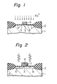
- a usual technique is used to form, on p type silicon semiconductor substrate 1, silicon dioxide field insulating layer 2, silicon dioxide gate insulating layer 3, and aluminum gate electrode 4.
- n + type source region 5 and n + type drain region 6 in silicon substrate 1.
- aluminum oxide layer 7 is formed on the surface of the aluminum gate electrode 4 by oxidation, for example utilizing the anode oxidation process.
- This oxidation process of aluminum may be carried out prior to the ion implanting process.
- a YAG laser beam having wavelength of 1.06 ⁇ m is irradiated onothe impurity doped regions' and the aluminum gate electrode to anneal source region 5 and drain region 6, producing a sheet resistivity of regions 5 and 6 of approximately 50 ⁇ / ⁇ . In this manner cracking can be avoided in aluminum gate electrode 4.
- a well known technique is used to form phosphosilicate glass layer 8 on the device shown in Fig. 2.
- An electrode contact hole is formed by patterning phosphosilicate glass layer 8 and silicon dioxide gate insulating layer 3.
- Source electrode 9 and drain electrode 10 are formed by patterning the aluminum layer.
- Phosphosilicate glass layer 11 is formed on source electrode 9, phosphosilicate glass layer 8, and drain electrode 10 and, thus, an integrated circuit (IC) chip is produced.
- a further contact hole may also be made to provide for electrical connection to the electrode.
- the aluminum oxide layer 7 may be changed to another insulating layer, for example, a silicon nitride layer or a silicon dioxide layer. Further, in addition to the anode oxidation process mentioned above, a plasma oxidation process, chemical vapor deposition process (CVD process) and so forth may be used to form aluminum oxide layer 7.
- thickness t of the insulating layer is equal to the value ⁇ m/2n; wherein n is the index of refraction of the insulating layer on the aluminum layer, ⁇ is the beam wavelength in a vacuum, and m is a positive integer.
- the data shown in Fig.4 was obtained by using a YAG laser having a wavelength of 1.06 ⁇ m.
- the thickness of the aluminum oxide layer should be 1960 ⁇ .
- the thickness of the aluminum oxide layer should be 2900 A. The above thicknesses of the aluminum oxide layers can be calculated from the formula, ⁇ m/2n.
- the thickness of the gate insulating layer should be formed to be ⁇ (2M-1) /4n'; wherein n' is the index of refraction of the gate insulating layer, ⁇ is a beam wavelength in a vacuum, and M is a positive integer.
- a laser beam in particular a ruby laser beam or YAG laser beam, was used as the beam by which impurity doped regions were annealed.
- a laser beam in particular a ruby laser beam or YAG laser beam
- an electron beam, lamp beam, and so forth may be used.
- At least the upper surface of the aluminum gate electrode is covered with an insulating layer of a thickness selected by the formula ⁇ m/2n so that the aluminum gate electrode can withstand the annealing, process whereby the source and drain regions are activated, with the result that a low sheet resistivity can be obtained.
- An embodiment of the present invention can thus be used for the production of a semiconductor device including an FET produced by the self-alignment method and using an aluminum gate electrode.
Landscapes
- Insulated Gate Type Field-Effect Transistor (AREA)
- Electrodes Of Semiconductors (AREA)
- Internal Circuitry In Semiconductor Integrated Circuit Devices (AREA)
- Thin Film Transistor (AREA)
Applications Claiming Priority (2)
| Application Number | Priority Date | Filing Date | Title |
|---|---|---|---|
| JP122657/81 | 1981-08-05 | ||
| JP56122657A JPS5823479A (ja) | 1981-08-05 | 1981-08-05 | 半導体装置の製造方法 |
Publications (3)
| Publication Number | Publication Date |
|---|---|
| EP0072216A2 true EP0072216A2 (fr) | 1983-02-16 |
| EP0072216A3 EP0072216A3 (en) | 1985-12-18 |
| EP0072216B1 EP0072216B1 (fr) | 1989-04-12 |
Family
ID=14841395
Family Applications (1)
| Application Number | Title | Priority Date | Filing Date |
|---|---|---|---|
| EP82304148A Expired EP0072216B1 (fr) | 1981-08-05 | 1982-08-05 | Procédé de fabrication de dispositifs semi-conducteurs comportant une étape de recuit |
Country Status (4)
| Country | Link |
|---|---|
| US (1) | US4468855A (fr) |
| EP (1) | EP0072216B1 (fr) |
| JP (1) | JPS5823479A (fr) |
| DE (1) | DE3279614D1 (fr) |
Cited By (13)
| Publication number | Priority date | Publication date | Assignee | Title |
|---|---|---|---|---|
| DE3342773A1 (de) * | 1983-11-25 | 1985-06-05 | Siemens AG, 1000 Berlin und 8000 München | Verfahren zum herstellen von spannungsfesten mos-feldeffekttransistoren mit weichen konzentrationsprofilen am drain-uebergang |
| US5308998A (en) * | 1991-08-26 | 1994-05-03 | Semiconductor Energy Laboratory Co., Ltd. | Insulated gate field effect semiconductor devices having a LDD region and an anodic oxide film of a gate electrode |
| US5401666A (en) * | 1992-06-17 | 1995-03-28 | Sony Corporation | Method for selective annealing of a semiconductor device |
| US5650338A (en) * | 1991-08-26 | 1997-07-22 | Semiconductor Energy Laboratory Co., Ltd. | Method for forming thin film transistor |
| USRE36314E (en) * | 1991-03-06 | 1999-09-28 | Semiconductor Energy Laboratory Co., Ltd. | Insulated gate field effect semiconductor devices having a LDD region and an anodic oxide film of a gate electrode |
| US6147375A (en) * | 1992-02-05 | 2000-11-14 | Semiconductor Energy Laboratory Co., Ltd. | Active matrix display device |
| US6323528B1 (en) | 1991-03-06 | 2001-11-27 | Semiconductor Energy Laboratory Co,. Ltd. | Semiconductor device |
| US6410374B1 (en) | 1992-12-26 | 2002-06-25 | Semiconductor Energy Laborartory Co., Ltd. | Method of crystallizing a semiconductor layer in a MIS transistor |
| US6489632B1 (en) | 1993-01-18 | 2002-12-03 | Semiconductor Energy Laboratory Co., Ltd. | Semiconductor device having a gate oxide film |
| US6544825B1 (en) | 1992-12-26 | 2003-04-08 | Semiconductor Energy Laboratory Co., Ltd. | Method of fabricating a MIS transistor |
| US6555843B1 (en) | 1991-05-16 | 2003-04-29 | Semiconductor Energy Laboratory Co., Ltd. | Semiconductor device and method for forming the same |
| US6867431B2 (en) | 1993-09-20 | 2005-03-15 | Semiconductor Energy Laboratory Co., Ltd. | Semiconductor device and method for manufacturing the same |
| US6964890B1 (en) | 1992-03-17 | 2005-11-15 | Semiconductor Energy Laboratory Co., Ltd. | Semiconductor device and method for forming the same |
Families Citing this family (62)
| Publication number | Priority date | Publication date | Assignee | Title |
|---|---|---|---|---|
| EP0058548B1 (fr) * | 1981-02-16 | 1986-08-06 | Fujitsu Limited | Procédé de fabrication d'un dispositif semiconducteur du type MOSFET |
| CA1186070A (fr) * | 1983-06-17 | 1985-04-23 | Iain D. Calder | Connexions de polysilicium faites au laser pour systemes a redondance |
| US4545823A (en) * | 1983-11-14 | 1985-10-08 | Hewlett-Packard Company | Grain boundary confinement in silicon-on-insulator films |
| US4727044A (en) | 1984-05-18 | 1988-02-23 | Semiconductor Energy Laboratory Co., Ltd. | Method of making a thin film transistor with laser recrystallized source and drain |
| US4621411A (en) * | 1984-09-28 | 1986-11-11 | Texas Instruments Incorporated | Laser-enhanced drive in of source and drain diffusions |
| US4749662A (en) * | 1984-12-14 | 1988-06-07 | Rockwell International Corporation | Diffused field CMOS-bulk process |
| JPS62177909A (ja) * | 1986-01-31 | 1987-08-04 | Hitachi Ltd | 半導体装置の製造方法 |
| US6008078A (en) | 1990-07-24 | 1999-12-28 | Semiconductor Energy Laboratory Co., Ltd. | Method for manufacturing a semiconductor device |
| JP2999271B2 (ja) * | 1990-12-10 | 2000-01-17 | 株式会社半導体エネルギー研究所 | 表示装置 |
| JP2739149B2 (ja) * | 1991-02-04 | 1998-04-08 | 株式会社 半導体エネルギー研究所 | 液晶表示装置 |
| JP2540688B2 (ja) * | 1991-08-23 | 1996-10-09 | 株式会社半導体エネルギー研究所 | 半導体装置とその作製方法 |
| JP2717234B2 (ja) * | 1991-05-11 | 1998-02-18 | 株式会社 半導体エネルギー研究所 | 絶縁ゲイト型電界効果半導体装置およびその作製方法 |
| JP2717233B2 (ja) * | 1991-03-06 | 1998-02-18 | 株式会社 半導体エネルギー研究所 | 絶縁ゲイト型電界効果半導体装置およびその作製方法 |
| JP3556679B2 (ja) * | 1992-05-29 | 2004-08-18 | 株式会社半導体エネルギー研究所 | 電気光学装置 |
| US6028333A (en) * | 1991-02-16 | 2000-02-22 | Semiconductor Energy Laboratory Co., Ltd. | Electric device, matrix device, electro-optical display device, and semiconductor memory having thin-film transistors |
| JPH05267666A (ja) * | 1991-08-23 | 1993-10-15 | Semiconductor Energy Lab Co Ltd | 半導体装置とその作製方法 |
| EP0499979A3 (en) | 1991-02-16 | 1993-06-09 | Semiconductor Energy Laboratory Co., Ltd. | Electro-optical device |
| US5468987A (en) * | 1991-03-06 | 1995-11-21 | Semiconductor Energy Laboratory Co., Ltd. | Semiconductor device and method for forming the same |
| US6713783B1 (en) | 1991-03-15 | 2004-03-30 | Semiconductor Energy Laboratory Co., Ltd. | Compensating electro-optical device including thin film transistors |
| JP2873632B2 (ja) * | 1991-03-15 | 1999-03-24 | 株式会社半導体エネルギー研究所 | 半導体装置 |
| JP2794499B2 (ja) | 1991-03-26 | 1998-09-03 | 株式会社半導体エネルギー研究所 | 半導体装置の作製方法 |
| JP3114963B2 (ja) * | 1991-05-16 | 2000-12-04 | 株式会社半導体エネルギー研究所 | 絶縁ゲイト型電界効果半導体装置 |
| US6778231B1 (en) | 1991-06-14 | 2004-08-17 | Semiconductor Energy Laboratory Co., Ltd. | Electro-optical display device |
| US6975296B1 (en) | 1991-06-14 | 2005-12-13 | Semiconductor Energy Laboratory Co., Ltd. | Electro-optical device and method of driving the same |
| US5414442A (en) * | 1991-06-14 | 1995-05-09 | Semiconductor Energy Laboratory Co., Ltd. | Electro-optical device and method of driving the same |
| JP2868168B2 (ja) * | 1991-08-23 | 1999-03-10 | 株式会社半導体エネルギー研究所 | 半導体装置の作製方法 |
| JP2845303B2 (ja) | 1991-08-23 | 1999-01-13 | 株式会社 半導体エネルギー研究所 | 半導体装置とその作製方法 |
| US6849872B1 (en) * | 1991-08-26 | 2005-02-01 | Semiconductor Energy Laboratory Co., Ltd. | Thin film transistor |
| US6979840B1 (en) * | 1991-09-25 | 2005-12-27 | Semiconductor Energy Laboratory Co., Ltd. | Thin film transistors having anodized metal film between the gate wiring and drain wiring |
| JP2750380B2 (ja) * | 1991-12-03 | 1998-05-13 | 株式会社 半導体エネルギー研究所 | 半導体装置の作製方法 |
| JP3277533B2 (ja) * | 1992-01-08 | 2002-04-22 | ソニー株式会社 | 半導体装置の製造方法 |
| TW223178B (en) * | 1992-03-27 | 1994-05-01 | Semiconductor Energy Res Co Ltd | Semiconductor device and its production method |
| US6624450B1 (en) | 1992-03-27 | 2003-09-23 | Semiconductor Energy Laboratory Co., Ltd. | Semiconductor device and method for forming the same |
| JP2742747B2 (ja) * | 1992-05-29 | 1998-04-22 | 株式会社半導体エネルギー研究所 | 薄膜トランジスタを有する多層半導体集積回路 |
| JP3252990B2 (ja) * | 1993-06-18 | 2002-02-04 | 株式会社半導体エネルギー研究所 | 半導体装置およびその作製方法 |
| JPH06124913A (ja) * | 1992-06-26 | 1994-05-06 | Semiconductor Energy Lab Co Ltd | レーザー処理方法 |
| US6624477B1 (en) | 1992-10-09 | 2003-09-23 | Semiconductor Energy Laboratory Co., Ltd. | Semiconductor device and method for manufacturing the same |
| US5576556A (en) * | 1993-08-20 | 1996-11-19 | Semiconductor Energy Laboratory Co., Ltd. | Thin film semiconductor device with gate metal oxide and sidewall spacer |
| TW232751B (en) | 1992-10-09 | 1994-10-21 | Semiconductor Energy Res Co Ltd | Semiconductor device and method for forming the same |
| JPH06232069A (ja) * | 1993-02-04 | 1994-08-19 | Semiconductor Energy Lab Co Ltd | 半導体装置の作製方法 |
| JPH0766152A (ja) * | 1993-08-30 | 1995-03-10 | Sony Corp | 半導体装置の製造方法 |
| US5719065A (en) | 1993-10-01 | 1998-02-17 | Semiconductor Energy Laboratory Co., Ltd. | Method for manufacturing semiconductor device with removable spacers |
| US5576231A (en) * | 1993-11-05 | 1996-11-19 | Semiconductor Energy Laboratory Co., Ltd. | Process for fabricating an insulated gate field effect transistor with an anodic oxidized gate electrode |
| US6943764B1 (en) | 1994-04-22 | 2005-09-13 | Semiconductor Energy Laboratory Co., Ltd. | Driver circuit for an active matrix display device |
| JP3402400B2 (ja) | 1994-04-22 | 2003-05-06 | 株式会社半導体エネルギー研究所 | 半導体集積回路の作製方法 |
| US6133620A (en) * | 1995-05-26 | 2000-10-17 | Semiconductor Energy Laboratory Co., Ltd. | Semiconductor device and process for fabricating the same |
| US6867432B1 (en) * | 1994-06-09 | 2005-03-15 | Semiconductor Energy Lab | Semiconductor device having SiOxNy gate insulating film |
| JP3330736B2 (ja) * | 1994-07-14 | 2002-09-30 | 株式会社半導体エネルギー研究所 | 半導体装置の作製方法 |
| JPH08248445A (ja) * | 1995-12-22 | 1996-09-27 | Semiconductor Energy Lab Co Ltd | 絶縁ゲイト型電界効果半導体装置 |
| JP2652364B2 (ja) * | 1995-12-22 | 1997-09-10 | 株式会社半導体エネルギー研究所 | 絶縁ゲイト型電界効果半導体装置およびその作製方法 |
| JP2715282B2 (ja) * | 1995-12-22 | 1998-02-18 | 株式会社半導体エネルギー研究所 | 絶縁ゲイト型電界効果半導体装置およびその作製方法 |
| JP3114964B2 (ja) * | 1995-12-22 | 2000-12-04 | 株式会社半導体エネルギー研究所 | 絶縁ゲイト型電界効果半導体装置の作製方法 |
| JP3565983B2 (ja) | 1996-04-12 | 2004-09-15 | 株式会社半導体エネルギー研究所 | 半導体装置の作製方法 |
| JP2652366B2 (ja) * | 1996-04-17 | 1997-09-10 | 株式会社半導体エネルギー研究所 | 半導体装置とその作製方法 |
| US6372592B1 (en) | 1996-12-18 | 2002-04-16 | United States Of America As Represented By The Secretary Of The Navy | Self-aligned MOSFET with electrically active mask |
| US6370502B1 (en) * | 1999-05-27 | 2002-04-09 | America Online, Inc. | Method and system for reduction of quantization-induced block-discontinuities and general purpose audio codec |
| US6245692B1 (en) * | 1999-11-23 | 2001-06-12 | Agere Systems Guardian Corp. | Method to selectively heat semiconductor wafers |
| JP2001313390A (ja) * | 2000-02-29 | 2001-11-09 | Agere Systems Inc | 半導体材料における選択的レーザ・アニール |
| KR100493382B1 (ko) * | 2002-08-28 | 2005-06-07 | 엘지.필립스 엘시디 주식회사 | 액정표시장치의 제조방법 |
| US9287405B2 (en) | 2011-10-13 | 2016-03-15 | Semiconductor Energy Laboratory Co., Ltd. | Semiconductor device comprising oxide semiconductor |
| US11069813B2 (en) * | 2019-09-30 | 2021-07-20 | Taiwan Semiconductor Manufacturing Co., Ltd. | Localized heating in laser annealing process |
| US11244907B2 (en) | 2020-01-02 | 2022-02-08 | International Business Machines Corporation | Metal surface preparation for increased alignment contrast |
Family Cites Families (6)
| Publication number | Priority date | Publication date | Assignee | Title |
|---|---|---|---|---|
| JPS50120365A (fr) * | 1974-03-05 | 1975-09-20 | ||
| US4243433A (en) * | 1978-01-18 | 1981-01-06 | Gibbons James F | Forming controlled inset regions by ion implantation and laser bombardment |
| DE2837653A1 (de) * | 1978-08-29 | 1980-04-17 | Siemens Ag | Verfahren zur lokal begrenzten erwaermung von festkoerpern |
| US4381201A (en) * | 1980-03-11 | 1983-04-26 | Fujitsu Limited | Method for production of semiconductor devices |
| US4284659A (en) * | 1980-05-12 | 1981-08-18 | Bell Telephone Laboratories | Insulation layer reflow |
| US4379727A (en) * | 1981-07-08 | 1983-04-12 | International Business Machines Corporation | Method of laser annealing of subsurface ion implanted regions |
-
1981
- 1981-08-05 JP JP56122657A patent/JPS5823479A/ja active Granted
-
1982
- 1982-08-04 US US06/405,269 patent/US4468855A/en not_active Expired - Lifetime
- 1982-08-05 DE DE8282304148T patent/DE3279614D1/de not_active Expired
- 1982-08-05 EP EP82304148A patent/EP0072216B1/fr not_active Expired
Cited By (26)
| Publication number | Priority date | Publication date | Assignee | Title |
|---|---|---|---|---|
| US7408233B2 (en) | 1919-01-18 | 2008-08-05 | Semiconductor Energy Laboratory Co., Ltd. | Semiconductor device having N-channel thin film transistor with LDD regions and P-channel thin film transistor with LDD region |
| DE3342773A1 (de) * | 1983-11-25 | 1985-06-05 | Siemens AG, 1000 Berlin und 8000 München | Verfahren zum herstellen von spannungsfesten mos-feldeffekttransistoren mit weichen konzentrationsprofilen am drain-uebergang |
| US6323528B1 (en) | 1991-03-06 | 2001-11-27 | Semiconductor Energy Laboratory Co,. Ltd. | Semiconductor device |
| US7569408B1 (en) | 1991-03-06 | 2009-08-04 | Semiconductor Energy Laboratory Co., Ltd. | Semiconductor device and method for forming the same |
| US5913112A (en) * | 1991-03-06 | 1999-06-15 | Semiconductor Energy Laboratory Co., Ltd. | Method of manufacturing an insulated gate field effect semiconductor device having an offset region and/or lightly doped region |
| USRE36314E (en) * | 1991-03-06 | 1999-09-28 | Semiconductor Energy Laboratory Co., Ltd. | Insulated gate field effect semiconductor devices having a LDD region and an anodic oxide film of a gate electrode |
| US6822261B2 (en) | 1991-03-06 | 2004-11-23 | Semiconductor Energy Laboratory Co., Ltd. | Semiconductor device and method for forming the same |
| US6555843B1 (en) | 1991-05-16 | 2003-04-29 | Semiconductor Energy Laboratory Co., Ltd. | Semiconductor device and method for forming the same |
| US6331723B1 (en) | 1991-08-26 | 2001-12-18 | Semiconductor Energy Laboratory Co., Ltd. | Active matrix display device having at least two transistors having LDD region in one pixel |
| US5650338A (en) * | 1991-08-26 | 1997-07-22 | Semiconductor Energy Laboratory Co., Ltd. | Method for forming thin film transistor |
| US7821011B2 (en) | 1991-08-26 | 2010-10-26 | Semiconductor Energy Laboratory Co., Ltd. | Insulated gate field effect semiconductor devices and method of manufacturing the same |
| US7456427B2 (en) | 1991-08-26 | 2008-11-25 | Semiconductor Energy Laboratory Co., Ltd. | Insulated gate field effect semiconductor devices and method of manufacturing the same |
| US5308998A (en) * | 1991-08-26 | 1994-05-03 | Semiconductor Energy Laboratory Co., Ltd. | Insulated gate field effect semiconductor devices having a LDD region and an anodic oxide film of a gate electrode |
| US6803600B2 (en) | 1991-08-26 | 2004-10-12 | Semiconductor Energy Laboratory Co., Ltd. | Insulated gate field effect semiconductor devices and method of manufacturing the same |
| US5962870A (en) * | 1991-08-26 | 1999-10-05 | Semiconductor Energy Laboratory Co., Ltd. | Insulated gate field effect semiconductor devices |
| US6476447B1 (en) | 1992-02-05 | 2002-11-05 | Semiconductor Energy Laboratory Co., Ltd. | Active matrix display device including a transistor |
| US6147375A (en) * | 1992-02-05 | 2000-11-14 | Semiconductor Energy Laboratory Co., Ltd. | Active matrix display device |
| US6964890B1 (en) | 1992-03-17 | 2005-11-15 | Semiconductor Energy Laboratory Co., Ltd. | Semiconductor device and method for forming the same |
| US7564057B1 (en) | 1992-03-17 | 2009-07-21 | Semiconductor Energy Laboratory Co., Ltd. | Semiconductor device having an aluminum nitride film |
| US5401666A (en) * | 1992-06-17 | 1995-03-28 | Sony Corporation | Method for selective annealing of a semiconductor device |
| US7351615B2 (en) | 1992-12-26 | 2008-04-01 | Semiconductor Energy Laboratory Co., Ltd. | Method of fabricating a MIS transistor |
| US6544825B1 (en) | 1992-12-26 | 2003-04-08 | Semiconductor Energy Laboratory Co., Ltd. | Method of fabricating a MIS transistor |
| US6410374B1 (en) | 1992-12-26 | 2002-06-25 | Semiconductor Energy Laborartory Co., Ltd. | Method of crystallizing a semiconductor layer in a MIS transistor |
| US6995432B2 (en) | 1993-01-18 | 2006-02-07 | Semiconductor Energy Laboratory Co., Ltd. | Semiconductor device having a gate oxide film with some NTFTS with LDD regions and no PTFTS with LDD regions |
| US6489632B1 (en) | 1993-01-18 | 2002-12-03 | Semiconductor Energy Laboratory Co., Ltd. | Semiconductor device having a gate oxide film |
| US6867431B2 (en) | 1993-09-20 | 2005-03-15 | Semiconductor Energy Laboratory Co., Ltd. | Semiconductor device and method for manufacturing the same |
Also Published As
| Publication number | Publication date |
|---|---|
| JPS5823479A (ja) | 1983-02-12 |
| DE3279614D1 (en) | 1989-05-18 |
| US4468855A (en) | 1984-09-04 |
| EP0072216A3 (en) | 1985-12-18 |
| EP0072216B1 (fr) | 1989-04-12 |
| JPS6259896B2 (fr) | 1987-12-14 |
Similar Documents
| Publication | Publication Date | Title |
|---|---|---|
| EP0072216A2 (fr) | Procédé de fabrication de dispositifs semi-conducteurs comportant une étape de recuit | |
| US4309224A (en) | Method for manufacturing a semiconductor device | |
| EP0058548B1 (fr) | Procédé de fabrication d'un dispositif semiconducteur du type MOSFET | |
| EP0315229B1 (fr) | Procédé pour la fabrication d'un dispositif à semi-conducteur à structure de la grille isolée | |
| US4267011A (en) | Method for manufacturing a semiconductor device | |
| US4384301A (en) | High performance submicron metal-oxide-semiconductor field effect transistor device structure | |
| US4512073A (en) | Method of forming self-aligned contact openings | |
| US5405804A (en) | Method of manufacturing a semiconductor device by laser annealing a metal layer through an insulator | |
| JPH0624226B2 (ja) | スタック形cmos装置の製造方法 | |
| JP3277533B2 (ja) | 半導体装置の製造方法 | |
| JP2509518B2 (ja) | チタニウムシリサイドコンタクト製造方法 | |
| US6544825B1 (en) | Method of fabricating a MIS transistor | |
| US4434013A (en) | Method of making a self-aligned Schottky metal semi-conductor field effect transistor with buried source and drain | |
| US5872047A (en) | Method for forming shallow junction of a semiconductor device | |
| US5225357A (en) | Low P+ contact resistance formation by double implant | |
| JP2864518B2 (ja) | 半導体装置の製造方法 | |
| EP0045593A2 (fr) | Procédé pour la fabrication d'un dispositif semi-conducteur | |
| US5683920A (en) | Method for fabricating semiconductor devices | |
| JPH07112063B2 (ja) | 電界効果トランジスタの製作方法 | |
| US7271041B2 (en) | Method for manufacturing thin film transistor | |
| US6040224A (en) | Method of manufacturing semiconductor devices | |
| JP3338182B2 (ja) | 半導体装置の作製方法 | |
| JP2948486B2 (ja) | 半導体素子の製造方法 | |
| JP3338434B2 (ja) | 薄膜トランジスタの作製方法 | |
| US5334543A (en) | Method of making reverse lightly doped drain (LDD) for buried N+ conductor |
Legal Events
| Date | Code | Title | Description |
|---|---|---|---|
| PUAI | Public reference made under article 153(3) epc to a published international application that has entered the european phase |
Free format text: ORIGINAL CODE: 0009012 |
|
| AK | Designated contracting states |
Designated state(s): DE FR GB |
|
| PUAL | Search report despatched |
Free format text: ORIGINAL CODE: 0009013 |
|
| AK | Designated contracting states |
Designated state(s): DE FR GB |
|
| 17P | Request for examination filed |
Effective date: 19860425 |
|
| 17Q | First examination report despatched |
Effective date: 19870701 |
|
| GRAA | (expected) grant |
Free format text: ORIGINAL CODE: 0009210 |
|
| AK | Designated contracting states |
Kind code of ref document: B1 Designated state(s): DE FR GB |
|
| REF | Corresponds to: |
Ref document number: 3279614 Country of ref document: DE Date of ref document: 19890518 |
|
| ET | Fr: translation filed | ||
| PLBE | No opposition filed within time limit |
Free format text: ORIGINAL CODE: 0009261 |
|
| STAA | Information on the status of an ep patent application or granted ep patent |
Free format text: STATUS: NO OPPOSITION FILED WITHIN TIME LIMIT |
|
| 26N | No opposition filed | ||
| PGFP | Annual fee paid to national office [announced via postgrant information from national office to epo] |
Ref country code: DE Payment date: 19931030 Year of fee payment: 12 |
|
| PG25 | Lapsed in a contracting state [announced via postgrant information from national office to epo] |
Ref country code: DE Effective date: 19950503 |
|
| PGFP | Annual fee paid to national office [announced via postgrant information from national office to epo] |
Ref country code: GB Payment date: 19990804 Year of fee payment: 18 |
|
| PGFP | Annual fee paid to national office [announced via postgrant information from national office to epo] |
Ref country code: FR Payment date: 19990810 Year of fee payment: 18 |
|
| PG25 | Lapsed in a contracting state [announced via postgrant information from national office to epo] |
Ref country code: GB Free format text: LAPSE BECAUSE OF NON-PAYMENT OF DUE FEES Effective date: 20000805 |
|
| GBPC | Gb: european patent ceased through non-payment of renewal fee |
Effective date: 20000805 |
|
| PG25 | Lapsed in a contracting state [announced via postgrant information from national office to epo] |
Ref country code: FR Free format text: LAPSE BECAUSE OF NON-PAYMENT OF DUE FEES Effective date: 20010430 |
|
| REG | Reference to a national code |
Ref country code: FR Ref legal event code: ST |