EP0077004B1 - Diode redresseuse à semi-conducteur - Google Patents
Diode redresseuse à semi-conducteur Download PDFInfo
- Publication number
- EP0077004B1 EP0077004B1 EP82109195A EP82109195A EP0077004B1 EP 0077004 B1 EP0077004 B1 EP 0077004B1 EP 82109195 A EP82109195 A EP 82109195A EP 82109195 A EP82109195 A EP 82109195A EP 0077004 B1 EP0077004 B1 EP 0077004B1
- Authority
- EP
- European Patent Office
- Prior art keywords
- semiconductor layer
- semiconductor
- type layer
- impurity concentration
- major surface
- Prior art date
- Legal status (The legal status is an assumption and is not a legal conclusion. Google has not performed a legal analysis and makes no representation as to the accuracy of the status listed.)
- Expired
Links
Images


Classifications
-
- H—ELECTRICITY
- H10—SEMICONDUCTOR DEVICES; ELECTRIC SOLID-STATE DEVICES NOT OTHERWISE PROVIDED FOR
- H10D—INORGANIC ELECTRIC SEMICONDUCTOR DEVICES
- H10D8/00—Diodes
-
- H—ELECTRICITY
- H10—SEMICONDUCTOR DEVICES; ELECTRIC SOLID-STATE DEVICES NOT OTHERWISE PROVIDED FOR
- H10D—INORGANIC ELECTRIC SEMICONDUCTOR DEVICES
- H10D62/00—Semiconductor bodies, or regions thereof, of devices having potential barriers
- H10D62/10—Shapes, relative sizes or dispositions of the regions of the semiconductor bodies; Shapes of the semiconductor bodies
- H10D62/124—Shapes, relative sizes or dispositions of the regions of semiconductor bodies or of junctions between the regions
- H10D62/125—Shapes of junctions between the regions
Definitions
- the present invention relates to a semiconductor rectifier diode.
- a rectifier diode to be used in the aforementioned power source is required to have a low loss, stability and a high speed. These characteristics have not been satisfied by the diodes which are well known in the art.
- the Shottky barrier diode as is disclosed in JP-A-55-107272 (1980), has had defects that the leakage current in the backward direction is high and that it is thermally unstable.
- the junction diode of p-i-n type has had a defect that its loss is not sufficiently low.
- this p-i-n type diode moreover, in order to enhance the low-loss character, there has been proposed an improvement for extremely reducing the thickness of the p- or h-type layer, as has been disclosed in IEEE Transactions on Electron Devices", Vol. ED-23, No. 8, August 1976, p. 945-949.
- the p-i-n type diode has had defects that it is difficult in production and bad in blocking voltage, yield and evenness.
- the FR-A-2456389 discloses a semiconductor rectifier diode having the features indicated in the preamble part of claim 1 of the present invention; but since the second main electrode thereof is a P + semiconductor layer forming potential barriers by contacting the third and fourth semiconductor layers and one of the outer periphery side ends of the third semiconductor layer is in direct contact with the fourth semiconductor layer, the forward voltage drop is relatively high, the reverse recovery time is relatively long, and a high blocking voltage cannot be obtained.
- Another object of the present invention is to provide a semiconductor rectifier diode which has such an improved structure as is easy in production and as is excellent in the low-loss, stability and high-speed characteristics. Said objects are achieved, according to the present invention, by a semiconductor rectifier diode comprising a semiconductor substrate having first and second major surfaces, positioned at opposite sides of said substrate, including a first semiconductor layer of n-conductivity type disposed adjacent to said first major surface, a second semiconductor layer of the n-conductivity type disposed adjacent to said first semiconductor layer and having a lower impurity concentration than said first semiconductor layer, a third semiconductor layer of a p conductivity type disposed adjacent to a selected portion of said second semiconductor layer and formed in said second major surface, said third semiconductor layer further having a higher impurity concentration than said second semiconductor layer, and at least one fourth semiconductor layer of the p conductivity type disposed adjacent to said second semiconductor layer and formed in said second major surface, having a smaller thickness in a direction normal to said second major surface of said substrate than said third semiconductor
- said fourth semiconductor layer has a plurality of stripes juxtaposed in one direction.
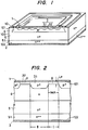
- Fig. 1 shows the overall construction and the section of a diode according to one embodiment of the present invention
- Fig. 2 is an enlarged view showing an essential portion in section.
- a semiconductor substrate 100 formed with a pair of main surfaces 101 and 102 has such a laminated structure between the paired main surfaces as is composed in succession of an n H- type layer 51, an n +- type layer 5, an n-type layer 4 and a p-type layer 3.
- This p-type layer 3 is so formed that first p-type layer portions 31 having a higher concentration and made thicker and second p-type layer portions 32 having a lower concentration and made thinner than the p-type layer portions 31 are arrayed alternately in respective stripe shapes.
- the second p-type layer portions 32 are substantially surrounded by the first p-type layer portions 31.
- Figs. 1 and 2 provide sections which are taken in directions perpendicular to the longitudinal directions of those stripe shapes.
- numerals I and 11 indicate first and second laminated structures, respectively.
- the p-type layer 3 has its terminal end exposed to the one main surface 101.
- the n +- layer 5 is exposed at the peripheral edge of the semiconductor substrate to the one main surface 101.
- the other main surface 102 of the semi-conductor substrate is formed with a cathode 2 which is made to ohmically contact with the n ++- type layer 51.
- the n +- type layer 5 has a high impurity concentration
- the n ++ -type layer 51 may be omitted, and the cathode 2 may be directly made to ohmically contact with the n +- type layer 5.
- the impurity concentration distribution of the first laminated structure in a direction normal to the main surfaces is plotted in a solid line in Fig. 3, whereas the impurity concentration distribution of the second laminated structure in the same direction as above is plotted in a broken line in the same Figure.
- the semiconductor substrate of the diode according to the present embodiment is sized to be a square having one side of about 4 mm.
- the diode of the present embodiment can be fabricated by making use of the well-known semiconductor device fabricating technique. The summary of one example will be described in the following.
- an n-n +- type silicon wafer is prepared. Phosphor is diffused selectively into one of the main surfaces of the wafer and wholly into the other main surface to form both the exposed portion of the n +- type layer 5 to the one main surface 101 and the n ++ -type layer 51.
- boron is selectively diffused into the one main surface to form the first p-type layer portion 31.
- boron ions are implanted into the one main surface, and a heat treatment is executed to form the second p-type layer portion 32.
- the paired main surfaces have their predetermined portions vacuum-evaporated with AI or a laminated film of Cr-Ni-Ag, for example, to form the anode 1 and the cathode 2.
- the Si0 2 film is either formed as a result of the oxidization of silicon during the aforementioned heat treatment such as a diffusion process or deposited by another CVD method.
- a main current flows between the paired main electrodes in a state (i.e., a forward bias state), in which a positive voltage is applied to the anode 1 relative to the cathode 2, but is blocked in a state (i.e., in a backward bias state) in which a negative voltage is applied to the anode 1 relative to the cathode 2.
- the main current passage is established mainly in the p-n-n +- n ++ diode region (i.e., the first laminated structure), including the second p-type layer portion 32.
- the second p-type layer portion 32 having a lower concentration and made thinner acts as a anode (or emitter) region to invite advantages such as a low loss and a high speed.
- the first p-type layer portion 31 made thicker bears the blocking voltage to invite advantages such as a high blocking voltage and stable characteristics.
- the depletion layer for pinching off the main current passage is formed of not the thinner second p-type layer portion 32 but the thicker first p-type layer portion 31, the design of the second p-type layer portion 32 of the main current passage can be advantageously conducted exclusively from the standpoint such as the low loss or the high speed, which is contrary to the high blocking voltage. Even if the second p-type layer portion 32 has defects such as pin holes, furthermore, there can be attained an effect that the reverse blocking voltage is not dropped. As a result, the production yield is enhanced.
- Fig. 4 plots the forward voltage drop of the p-type layer portion 32 of the diode of the present embodiment against a width Wch
- Fig. 5 plots the blocking voltage against the width Wch.
- the current density is about 60 A/cm 2
- the thickness Lp of the second p-type layer portion 32 is 2 um
- the thickness of the first p-type layer portion 31 is 5 pm
- the thickness of the n-type layer 4 between the bottom of the first p-type layer portion 31 and the n +- type layer 5 is 5 ⁇ m.
- the forward voltage drop is merely increased by about 0.02 V but the blocking voltage can be raised by about 70 V by reducing the width of the second p-type layer portion 32 from about 10 ⁇ m to about 2 um, for example, even if the second p-type layer portion 32 has the low surface impurity concentration of 5x 10 15 cm- 3 and the small thickness of 2 um.
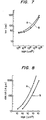
- Figs. 6, 7 and 8 plot the forward voltage drop, the backward restoration time t rr and the reduction rate di R /dt of the backward restoration current, respectively, in case the thickness Lp of the second p-type layer portion 32 is 1 to 2 ⁇ m whereas the impurity concentration Nn of the n-type layer 4 is 1 x 10 14 to 1 x10 15 cm-3.
- Those plots correspond to the case in which the forward current density is about 60 Alcm 2 and the forward current reduction rate during the backward restoration is 30 Alps.
- the thickness Lp and the impurity concentration Nn of those respective Figures take such values as are tabulated in Table 2.
- the forward voltage drop can be reduced, the backward restoration can be accelerated and the backward restoration characteristics can be made soft (in other words, the rate di R /dt can be decelerated) by reducing the surface impurity concentration.
- the second p-type layer portion 32 is made to have a thickness of 1 to 2 pm and a surface impurity concentration of 1x10 15 to 1x10 16 cm- 3 , for example, the forward voltage drop, the backward restoration time t rr and the backward restoration current reduction rate di R /dt can be reduced to 0.68 to 0.69 V, 35 to 40 ns, and 12 to 20 A/ ⁇ s, respectively, thereby to provide a high-speed rectifier diode having a high performance.
- the impurity concentration of the second p-type layer portion 32 As the impurity concentration of the second p-type layer portion 32 is lowered, the positive holes are to be injected into the n-type layer 4 from the second p-type layer portion 32 in the forward bias state so that the current through the n-type layer 4 is a flow of the electrons acting as major carriers. As a result, the backward restoration time t rr is shortened. As the impurity concentration of the second p-type layer portion 32 is lowered, on the other hand, the diffusion potential at the pn junction is accordingly lowered to reduce the forward voltage drop.
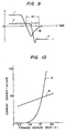
- Fig. 9 illustrates the waveforms of a current i and a voltage v when the diode is reversed from its forward state.
- a backward restoration current i R flows, too, even after the bias has been reversed.
- the backward restoration current i R itself be small, it is important for the low power loss that the power loss (vxi) during the period, as indicated at t d , be low. Especially large consideration should be taken into that power loss because this loss grows higher than any other loss during a high-frequency operation higher than about 50 Hz.
- the reduction rate di R /dt be low (in other words, to have soft recovery characteristics). Since the reduction rate di R /dt is low according to the present embodiment, the aforementioned power loss is so low that the present embodiment finds its suitable application in a switching regulator.
- Fig. 10 plots the relationship in the forward voltage drop and the forward current between the present embodiment (A) and the Shottky barrier diode (B).
- the sample B has its base layer thickness adjusted to have a blocking voltage of 150 V.
- the sample A exhibits a lower forward voltage drop than the sample B in the range where the current density in the forward direction is equal to or higher than about 50 A/cm 2 . Within the range of the practically used current density (equal to or higher than 100 A/cm 2 ), therefore, the diode of the present embodiment has a lower loss than the Shottky barrier diode.
- the diode of the present embodiment is far superior in the backward leakage current characteristics to the Schottky barrier diode.
Landscapes
- Electrodes Of Semiconductors (AREA)
- Bipolar Transistors (AREA)
Claims (2)
Applications Claiming Priority (2)
| Application Number | Priority Date | Filing Date | Title |
|---|---|---|---|
| JP158758/81 | 1981-10-07 | ||
| JP56158758A JPS5860577A (ja) | 1981-10-07 | 1981-10-07 | 半導体装置 |
Publications (3)
| Publication Number | Publication Date |
|---|---|
| EP0077004A2 EP0077004A2 (fr) | 1983-04-20 |
| EP0077004A3 EP0077004A3 (en) | 1985-09-18 |
| EP0077004B1 true EP0077004B1 (fr) | 1990-02-07 |
Family
ID=15678695
Family Applications (1)
| Application Number | Title | Priority Date | Filing Date |
|---|---|---|---|
| EP82109195A Expired EP0077004B1 (fr) | 1981-10-07 | 1982-10-05 | Diode redresseuse à semi-conducteur |
Country Status (3)
| Country | Link |
|---|---|
| EP (1) | EP0077004B1 (fr) |
| JP (1) | JPS5860577A (fr) |
| DE (1) | DE3280111D1 (fr) |
Cited By (1)
| Publication number | Priority date | Publication date | Assignee | Title |
|---|---|---|---|---|
| DE3631136A1 (de) * | 1986-09-12 | 1988-03-24 | Siemens Ag | Diode mit weichem abrissverhalten |
Families Citing this family (16)
| Publication number | Priority date | Publication date | Assignee | Title |
|---|---|---|---|---|
| JPS5929469A (ja) * | 1982-08-11 | 1984-02-16 | Hitachi Ltd | 半導体装置 |
| JPS60140768A (ja) * | 1983-12-28 | 1985-07-25 | Toyo Electric Mfg Co Ltd | 整流素子 |
| FR2578101B1 (fr) * | 1985-02-26 | 1987-10-09 | Thomson Csf | Diode hyperfrequence de type pin a transitions abruptes |
| JPS62115880A (ja) * | 1985-11-15 | 1987-05-27 | Shindengen Electric Mfg Co Ltd | Pn接合素子 |
| JP2590284B2 (ja) * | 1990-02-28 | 1997-03-12 | 株式会社日立製作所 | 半導体装置及びその製造方法 |
| US5278443A (en) * | 1990-02-28 | 1994-01-11 | Hitachi, Ltd. | Composite semiconductor device with Schottky and pn junctions |
| US5166760A (en) * | 1990-02-28 | 1992-11-24 | Hitachi, Ltd. | Semiconductor Schottky barrier device with pn junctions |
| DE4201183A1 (de) * | 1992-01-17 | 1993-07-22 | Eupec Gmbh & Co Kg | Leistungsdiode |
| JP2719295B2 (ja) * | 1993-04-09 | 1998-02-25 | リコー応用電子研究所株式会社 | 半導体整流装置 |
| JP4857484B2 (ja) * | 2001-04-20 | 2012-01-18 | 富士電機株式会社 | 半導体装置およびその製造方法 |
| JP2003338620A (ja) * | 2002-05-22 | 2003-11-28 | Mitsubishi Electric Corp | 半導体装置およびその製造方法 |
| JP2005191227A (ja) * | 2003-12-25 | 2005-07-14 | Sanyo Electric Co Ltd | 半導体装置 |
| JP5306392B2 (ja) | 2011-03-03 | 2013-10-02 | 株式会社東芝 | 半導体整流装置 |
| JP2013243186A (ja) * | 2012-05-18 | 2013-12-05 | Origin Electric Co Ltd | 半導体素子 |
| JP5865860B2 (ja) * | 2013-03-25 | 2016-02-17 | 株式会社東芝 | 半導体装置 |
| CN110534583B (zh) * | 2019-08-01 | 2023-03-28 | 山东天岳电子科技有限公司 | 一种肖特基二极管及其制备方法 |
Family Cites Families (5)
| Publication number | Priority date | Publication date | Assignee | Title |
|---|---|---|---|---|
| DE2457106A1 (de) * | 1974-12-03 | 1976-06-10 | Siemens Ag | Thyristor |
| JPS5935183B2 (ja) * | 1975-08-20 | 1984-08-27 | サンケイ電気 (株) | シヨツトキバリア半導体装置 |
| DE2807785A1 (de) * | 1978-02-23 | 1979-08-30 | Siemens Ag | Digitales nachrichtenuebertragungssystem |
| GB2050694B (en) * | 1979-05-07 | 1983-09-28 | Nippon Telegraph & Telephone | Electrode structure for a semiconductor device |
| US4278476A (en) * | 1979-12-05 | 1981-07-14 | Westinghouse Electric Corp. | Method of making ion implanted reverse-conducting thyristor |
-
1981
- 1981-10-07 JP JP56158758A patent/JPS5860577A/ja active Pending
-
1982
- 1982-10-05 EP EP82109195A patent/EP0077004B1/fr not_active Expired
- 1982-10-05 DE DE8282109195T patent/DE3280111D1/de not_active Expired - Lifetime
Cited By (1)
| Publication number | Priority date | Publication date | Assignee | Title |
|---|---|---|---|---|
| DE3631136A1 (de) * | 1986-09-12 | 1988-03-24 | Siemens Ag | Diode mit weichem abrissverhalten |
Also Published As
| Publication number | Publication date |
|---|---|
| DE3280111D1 (de) | 1990-03-15 |
| EP0077004A3 (en) | 1985-09-18 |
| EP0077004A2 (fr) | 1983-04-20 |
| JPS5860577A (ja) | 1983-04-11 |
Similar Documents
| Publication | Publication Date | Title |
|---|---|---|
| US7276771B2 (en) | Diode and method for manufacturing the same | |
| KR920010677B1 (ko) | 반도체장치 | |
| CN108074924B (zh) | 半导体装置 | |
| EP0707744B1 (fr) | Diode de redressement de schottky a tranchee mos | |
| EP0077004A2 (fr) | Diode redresseuse à semi-conducteur | |
| EP0205217A2 (fr) | Dispositifs semi-conducteurs | |
| EP0634796B1 (fr) | Transistor bipolaire à grille isolée | |
| JP2000323488A (ja) | ダイオードおよびその製造方法 | |
| JPH0642542B2 (ja) | 高耐圧半導体装置の製造方法 | |
| US5414290A (en) | IGBT with self-aligning cathode pattern and method for producing it | |
| US6734520B2 (en) | Semiconductor component and method of producing it | |
| US4901120A (en) | Structure for fast-recovery bipolar devices | |
| EP0103138B1 (fr) | Diode redresseuse semi-conductrice | |
| JPH07226521A (ja) | 整流用半導体装置 | |
| EP1376703A2 (fr) | Dispositif semi-conducteur à grille isolée et sa méthode de fabrication | |
| US6160306A (en) | Diode of semiconductor device and method for manufacturing the same | |
| GB2082836A (en) | Corrugated semiconductor devices | |
| JPH0266977A (ja) | 半導体ダイオード | |
| JPH033954B2 (fr) | ||
| JPH0286173A (ja) | 半導体ダイオード | |
| GB2306046A (en) | Semiconductor device with a concave junction | |
| KR102783636B1 (ko) | SiC 쇼트키 다이오드 소자 및 그 제조 방법 | |
| KR20190127323A (ko) | 반도체 소자 및 그 제조 방법 | |
| KR830001930B1 (ko) | 반도체장치의 전극구조 | |
| JP2002118115A (ja) | 半導体装置およびその製造方法 |
Legal Events
| Date | Code | Title | Description |
|---|---|---|---|
| PUAI | Public reference made under article 153(3) epc to a published international application that has entered the european phase |
Free format text: ORIGINAL CODE: 0009012 |
|
| AK | Designated contracting states |
Designated state(s): DE FR GB NL |
|
| PUAL | Search report despatched |
Free format text: ORIGINAL CODE: 0009013 |
|
| AK | Designated contracting states |
Designated state(s): DE FR GB NL |
|
| 17P | Request for examination filed |
Effective date: 19850919 |
|
| 17Q | First examination report despatched |
Effective date: 19861027 |
|
| R17C | First examination report despatched (corrected) |
Effective date: 19870706 |
|
| GRAA | (expected) grant |
Free format text: ORIGINAL CODE: 0009210 |
|
| AK | Designated contracting states |
Kind code of ref document: B1 Designated state(s): DE NL |
|
| REF | Corresponds to: |
Ref document number: 3280111 Country of ref document: DE Date of ref document: 19900315 |
|
| EN | Fr: translation not filed | ||
| PLBE | No opposition filed within time limit |
Free format text: ORIGINAL CODE: 0009261 |
|
| STAA | Information on the status of an ep patent application or granted ep patent |
Free format text: STATUS: NO OPPOSITION FILED WITHIN TIME LIMIT |
|
| 26N | No opposition filed | ||
| PGFP | Annual fee paid to national office [announced via postgrant information from national office to epo] |
Ref country code: NL Payment date: 19971031 Year of fee payment: 16 |
|
| PGFP | Annual fee paid to national office [announced via postgrant information from national office to epo] |
Ref country code: DE Payment date: 19981231 Year of fee payment: 17 |
|
| PG25 | Lapsed in a contracting state [announced via postgrant information from national office to epo] |
Ref country code: NL Free format text: LAPSE BECAUSE OF NON-PAYMENT OF DUE FEES Effective date: 19990501 |
|
| NLV4 | Nl: lapsed or anulled due to non-payment of the annual fee |
Effective date: 19990501 |
|
| PG25 | Lapsed in a contracting state [announced via postgrant information from national office to epo] |
Ref country code: DE Free format text: LAPSE BECAUSE OF NON-PAYMENT OF DUE FEES Effective date: 20000801 |