EP0077200A2 - Procédé pour la formation de couches isolantes dans des dispositifs semiconducteurs - Google Patents
Procédé pour la formation de couches isolantes dans des dispositifs semiconducteurs Download PDFInfo
- Publication number
- EP0077200A2 EP0077200A2 EP82305379A EP82305379A EP0077200A2 EP 0077200 A2 EP0077200 A2 EP 0077200A2 EP 82305379 A EP82305379 A EP 82305379A EP 82305379 A EP82305379 A EP 82305379A EP 0077200 A2 EP0077200 A2 EP 0077200A2
- Authority
- EP
- European Patent Office
- Prior art keywords
- layer
- silicon
- oxide
- substrate
- tantalum
- Prior art date
- Legal status (The legal status is an assumption and is not a legal conclusion. Google has not performed a legal analysis and makes no representation as to the accuracy of the status listed.)
- Granted
Links
Images


Classifications
-
- H—ELECTRICITY
- H10—SEMICONDUCTOR DEVICES; ELECTRIC SOLID-STATE DEVICES NOT OTHERWISE PROVIDED FOR
- H10P—GENERIC PROCESSES OR APPARATUS FOR THE MANUFACTURE OR TREATMENT OF DEVICES COVERED BY CLASS H10
- H10P14/00—Formation of materials, e.g. in the shape of layers or pillars
- H10P14/60—Formation of materials, e.g. in the shape of layers or pillars of insulating materials
- H10P14/69—Inorganic materials
- H10P14/692—Inorganic materials composed of oxides, glassy oxides or oxide-based glasses
- H10P14/6938—Inorganic materials composed of oxides, glassy oxides or oxide-based glasses the material containing at least one metal element, e.g. metal oxides, metal oxynitrides or metal oxycarbides
- H10P14/6939—Inorganic materials composed of oxides, glassy oxides or oxide-based glasses the material containing at least one metal element, e.g. metal oxides, metal oxynitrides or metal oxycarbides characterised by the metal
- H10P14/69393—Inorganic materials composed of oxides, glassy oxides or oxide-based glasses the material containing at least one metal element, e.g. metal oxides, metal oxynitrides or metal oxycarbides characterised by the metal the material containing tantalum, e.g. Ta2O5
-
- H—ELECTRICITY
- H10—SEMICONDUCTOR DEVICES; ELECTRIC SOLID-STATE DEVICES NOT OTHERWISE PROVIDED FOR
- H10P—GENERIC PROCESSES OR APPARATUS FOR THE MANUFACTURE OR TREATMENT OF DEVICES COVERED BY CLASS H10
- H10P14/00—Formation of materials, e.g. in the shape of layers or pillars
- H10P14/60—Formation of materials, e.g. in the shape of layers or pillars of insulating materials
- H10P14/63—Formation of materials, e.g. in the shape of layers or pillars of insulating materials characterised by the formation processes
- H10P14/6302—Non-deposition formation processes
- H10P14/6304—Formation by oxidation, e.g. oxidation of the substrate
- H10P14/6306—Formation by oxidation, e.g. oxidation of the substrate of the semiconductor materials
- H10P14/6308—Formation by oxidation, e.g. oxidation of the substrate of the semiconductor materials of Group IV semiconductors
- H10P14/6309—Formation by oxidation, e.g. oxidation of the substrate of the semiconductor materials of Group IV semiconductors of silicon in uncombined form, i.e. pure silicon
-
- H—ELECTRICITY
- H10—SEMICONDUCTOR DEVICES; ELECTRIC SOLID-STATE DEVICES NOT OTHERWISE PROVIDED FOR
- H10P—GENERIC PROCESSES OR APPARATUS FOR THE MANUFACTURE OR TREATMENT OF DEVICES COVERED BY CLASS H10
- H10P14/00—Formation of materials, e.g. in the shape of layers or pillars
- H10P14/60—Formation of materials, e.g. in the shape of layers or pillars of insulating materials
- H10P14/63—Formation of materials, e.g. in the shape of layers or pillars of insulating materials characterised by the formation processes
- H10P14/6302—Non-deposition formation processes
- H10P14/6304—Formation by oxidation, e.g. oxidation of the substrate
- H10P14/6314—Formation by oxidation, e.g. oxidation of the substrate of a metallic layer
-
- H—ELECTRICITY
- H10—SEMICONDUCTOR DEVICES; ELECTRIC SOLID-STATE DEVICES NOT OTHERWISE PROVIDED FOR
- H10P—GENERIC PROCESSES OR APPARATUS FOR THE MANUFACTURE OR TREATMENT OF DEVICES COVERED BY CLASS H10
- H10P14/00—Formation of materials, e.g. in the shape of layers or pillars
- H10P14/60—Formation of materials, e.g. in the shape of layers or pillars of insulating materials
- H10P14/63—Formation of materials, e.g. in the shape of layers or pillars of insulating materials characterised by the formation processes
- H10P14/6302—Non-deposition formation processes
- H10P14/6322—Formation by thermal treatments
-
- H—ELECTRICITY
- H10—SEMICONDUCTOR DEVICES; ELECTRIC SOLID-STATE DEVICES NOT OTHERWISE PROVIDED FOR
- H10P—GENERIC PROCESSES OR APPARATUS FOR THE MANUFACTURE OR TREATMENT OF DEVICES COVERED BY CLASS H10
- H10P14/00—Formation of materials, e.g. in the shape of layers or pillars
- H10P14/60—Formation of materials, e.g. in the shape of layers or pillars of insulating materials
- H10P14/65—Formation of materials, e.g. in the shape of layers or pillars of insulating materials characterised by treatments performed before or after the formation of the materials
- H10P14/6516—Formation of materials, e.g. in the shape of layers or pillars of insulating materials characterised by treatments performed before or after the formation of the materials of treatments performed after formation of the materials
- H10P14/6529—Formation of materials, e.g. in the shape of layers or pillars of insulating materials characterised by treatments performed before or after the formation of the materials of treatments performed after formation of the materials by exposure to a gas or vapour
-
- H—ELECTRICITY
- H10—SEMICONDUCTOR DEVICES; ELECTRIC SOLID-STATE DEVICES NOT OTHERWISE PROVIDED FOR
- H10P—GENERIC PROCESSES OR APPARATUS FOR THE MANUFACTURE OR TREATMENT OF DEVICES COVERED BY CLASS H10
- H10P14/00—Formation of materials, e.g. in the shape of layers or pillars
- H10P14/60—Formation of materials, e.g. in the shape of layers or pillars of insulating materials
- H10P14/66—Formation of materials, e.g. in the shape of layers or pillars of insulating materials characterised by the type of materials
- H10P14/662—Laminate layers, e.g. stacks of alternating high-k metal oxides
Definitions
- the present invention relates to the production of insulating layers in semiconductor devices.
- Dieletric layers are essential features of some semiconductor devices, for example, gate insulating layers in field effect transistors and dielectric layers of capacitors. Such devices may be included in components comprising transistor-diode logic, transistor- transistor logic, read only memory, or dynamic random access memory.
- the capacitance of capacitors is proportional to the relative dielectric constant of the dielectric material inserted between electrodes and inversely proportional to the distance between the electrodes.
- the trans conductance gm of field effect transistors is also proportional to the relative dielectric constant of the gate--insulating dielectric layer and inversely proportional to the thickness of the layer.
- Silicon dioxide (Si0 2 ) layers have been mainly used as dielectric layers, the functions of which are set forth above, based on the fact that silicon dioxide has a relative dielectric constant of 3.8 and a dielectric breakdown voltage of 10 MV/cm. However, it has been found difficult to form a silicon dioxide layer the thickness of which is less than 10nm without pinholes which will inevitably lead to an increased leakage of current, and, consequently, a lower breakdown voltage.
- tantalum oxide exhibits a relative dielectric constant of from 20 to 28.
- each of these dielectric oxides has disadvantages in tnat the breakdown voltage is low and the leakage of current is large.
- these disadvantages may be reduced by thickening the dielectric layer, but this leads to unfavorable lowering of the capacitance.
- a Ta 2 O 5 /SiO 2 double layer may be used in which a silicon dioxide layer is first formed on a substrate and then a tantalum oxide (Ta 2 O 5 ) layer is formed thereon so as to form the Ta 2 O 5 /SiO 2 double layer.
- such a Ta 2 O 5 /SiO 2 double structure exhibits a disadvantage in that the capacitance is low due to the thickness of the oxidized silicon, which thickness cannot be reduced owing to the occurrence of pin holes, as mentioned above. Furthermore, the electrical properties of the previously formed silicon dioxide layer deteriorate during the formation of tantalum oxide thereon, thereby lowering the breakdown voltage. In addition, such a double structure exhibits an unfavorable hysteresis in respect to the capacitance-voltage characteristic of a diode due to the abrupt heterojunction thereof.
- a method-of manufacturing a semiconductor device wherein a layer of an oxide of an element selected from the group made up of tantalum, titanium, niobium, hafnium, yttrium, zirconium, and vanadium is formed on a semi- conductor substrate characterized in that the said semiconductor substrate having said layer of oxide thereon is heated in an oxidizing atmosphere so as to oxidize semiconductor material of the said substrate thereby to form an insulating layer made of an oxide of said semi- conductor material, sandwiched between said layer of oxide and remaining semiconductor material of the said substrate.
- the oxide layer comprises a tantalum oxide layer
- the semiconductor layer may advantageously be made of silicon.
- said oxidizing atmosphere comprises wet oxygen and the oxidization is carried out at at a temperature in a range from 700°C to 1200°C.
- a preferred embodiment of the present invention provides a process for producing a dielectric layer on a silicon semiconductor layer, characterized by the steps of:
- said silicon semiconductor layer is of a one-conductivity type.
- said process can further comprise the step of forming an electrically conductive layer on said tantalum oxide layer.
- An embodiment of the present invention can provide a process for producing a dielectric layer having a desirably high relative dielectric constant, a relatively high dielectric breakdown voltage, and desirably small current leakage.
- a dielectric layer can be made to exhibit very low hysteresis in respect to the capacitance-voltage characteristic of a diode.
- a high dielectric layer (2 1 ), e.g., tantalum oxide (Ta205), may be formed on a semiconductor substrate (1) either by an indirect process, e.g., first depositing tantalum (2) by vacuum vapor deposition or sputtering (Fig. la) and then oxidizing tantalum into tantalum oxide (2'), or by a direct process, e.g., chemical vapor deposition or oxide sputtering (Fig. lb).
- the thus--obtained oxide may be further subjected to a thermal treatment, whereby the oxide may be crystallized and improved in respect to thermal stability.
- the low breakdown voltage of the tantalum oxide (2') is compensated for by heating the substrate (1) in an oxidizing atmosphere so as to form a layer of oxide of the semiconductor material (3), e.g., silicon oxide, mainly at the interface between the semiconductor substrate (1) and the tantalum oxide (2') (Fig. lc).
- a layer of oxide of the semiconductor material (3) e.g., silicon oxide
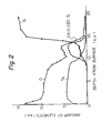
- the thus-formed composite oxide layer is better illustrated in Fig. 2.
- the composition was determined by the Auger sputtering method. At the end of the tantalum region, the silicon shifted in a combined state with the oxygen (Fig. 2).
- the total thickness of the oxide layer was determined by the Talystep method before and after oxidation and then the difference in thickness was assumed to be the thickness of oxidized silicon.
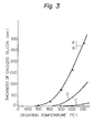
- a silicon substrate coated with tantalum oxide 45 nm thick (A) and a bare silicon substrate B were oxidized.in wet oxygen (Fig. 3).
- a silicon substrate coated with tantalum oxide 24 nm thick (C) and a bare silicon substrate (D) were oxidized in dry oxygen (Fig. 3). These thermal treatments were continued for 30 minutes at various temperatures.
- the substrates (A, B) were oxidized quickly in wet oxygen without regarding the coating of tantalum oxide and were effective at a temperature higher than 700°C. Contrary to this, the substrates (C, D) were oxidized slowly in dry oxygen, particularly in the case coated with tantalum oxide, and were oxidized only at a temperature higher than 900°C. An oxidation temperature higher than 1200°C exhibited no advantages in respect to the consumption of energy in relation to either wet or dry oxidation.
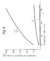
- the thickness of the oxidized silicon gradually increased as heating of the silicon semiconductor substrates A, B, C, and D used in the experiment of Fig. 3 was continued (Fig. 4). These substrates A, B, C, and D were heated at 1000°C. Wet oxidation (A, B) was superior to dry oxidation (C, D) in respect to their growth.
- oxygen in a wet oxygen atmosphere diffuses freely through the tantalum oxide layer. Contrary to this, oxygen in a dry oxygen atmosphere scarcely diffuses therethrough. Furthermore, it was confirmed that oxygen in a wet oxygen atmosphere diffuses several ⁇ m laterally through a tantalum layer 45 nm thick.
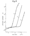
- a silicon substrate coated with tantalum oxide 45 nm thick was heated in wet oxygen at 800°C. Oxidation was continued for 10 minutes (F), 20 minutes (G) and 30 minutes (H) (Fig. 5). Thus, the silicon at the interface was oxidized so as to produce a dielectric layer according to the present invention.
- double oxide layer produced in a method embodying the present invention can exhibit a high dielectric constant and a high breakdown voltage.
- a layer of tantalum 15 nm thick (2) was deposited on a silicon substrate (1) by RF sputtering in argon at 4 x 10 -2 Torr (Fig. la).
- the substrate (1) was heated in dry oxygen at 525°C for 40 minutes. As a result, a tantalum oxide (2') layer 33 nm thick was formed (Fig. lb).
- the substrate (1) having a tantalum oxide layer (2') thereon was heated in wet oxygen at 800°C for 13 minutes.
- Oxide layers (3) comprising silicon oxide were produced mainly under the tantalum oxide layer, i.e., the thickness of the silicon oxide was 0.3 nm on the surface and 5 nm at the interface between the tantalum oxide layer (2') and the silicon substrate (1), respectively (Fig. lc).
- a very thin silicon oxide layer (not shown) was formed on the surface of the tantalum oxide layer (2') during oxidation in a wet oxygen atmosphere.
- the substrate was annealed in nitrogen containing 5% by volume of hydrogen at 1050°C for 30 minutes and then electrodes were produced (not shown).
- the thus-obtained dielectric layer composite having silicon oxide in addition to tantalum oxide . exhibited a relative dielectric constant of 15, a dielectric breakdown voltage of 4 MV/cm, and a leakage current on the order of 10 -10 A at 5 V.
- the relative dielectric constant was more than three times greater than that of silicon oxide, and the breakdown voltage was several times greater than that of tantalum oxide.
- this composite exhibited no hysteresis in respect to the capacitance-voltage characteristic of a diode.
- the amount of silicon contained in an electrode of silicide of a high melting point metal, e.g., molybdenum silicide, which is formed on the tantalum oxide layer not exceed the stoichiometry ratio.
- MoSi 2 satisfies the stoichiometry ratio, i.e., it does not discharge silicon atoms.
- Molybdenum atoms which pile up from a MoSi layer do not react with Ta 2 0 5 , which is thermodynamically stable in the Mo - Ta 2 O 5 system.
- the upper electrode 4 of the molybdenum silicide layer formed on the tantalum oxide layer 3 must not contain silicon in an amount in excess of the stoichiometry ratio.
- silicide-oxide systems which comprises silicide, e.g., of tungsten, tantalum, or platinum and oxide of a metal in the group 3A, 4A, or 5A of the periodic table of elements.
- Figures 6 through 12 are diagrams showing the steps for producing a dynamic random access memory device by a - method embodying the present invention.
- Field oxide layers (12) 1 ⁇ m thick were produced on a p type silicon semiconductor substrate (11) in a usual manner.
- a tantalum layer (13) 20 nm thick was produced on the substrate by RF sputtering in argon at 4 x 10 -2 Torr with an accerelating voltage of 2.3 KV (Fig. 6).
- the tantalum layer (13) was converted to a tantalum oxide layer (13') 44 nm thick by heating it at 500°C and then heating the substrate (11) at 800°C in wet oxygen, and thereby a silicon oxide layer (14) 6 nm thick was produced at the interface between the silicon substrate (11) and the tantalum oxide layer (13') (Fig. 7).
- a molybdenum (Mo) or molybdenum silicide electrode (15) for capacitor electrode was sputtered on the tantalum oxide layer (13') and then an insulating layer (16) of silicon oxide was deposited by chemical vapor deposition (Fig. 8).
- the insulating layer (16), the capacitor electrode (15), and the tantalum oxide layer (13') were partly removed by dry etching with a CHF 3 etchant, thus partially exposing the silicon oxide layer (14) at the interface (Fig. 9).
- a silicon oxide layer (17) was further deposited by chemical vapor deposition (Fig. 10).
- the silicon oxide layer (17) was removed, except for the portion coating the side surface (side wall) of the capacitor electrode (15), by dry etching.
- a transfer gate insulating layer (18) 40 nm thick was formed on the silicon substrate (11) by thermal oxidation (Fig. ll).
- a transfer gate electrode (19) was formed by depositing and patterning polycrystalline silicon. Then, a n type bit line contact region (20) was formed by arsenic (As) ion implantation, whereby arsenic was implanted into the transfer gate electrode (19). An electrode contact window was opened by forming and patterning the silicon oxide layer (21). A bit line (22) was formed by depositing and patterning an aluminum layer (Fig. 12).
- the thus-obtained dynamic random access memory device exhibited a significantly small leakage current and a higher integration.
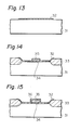
- Figures 13 through 16 are diagrams showing the steps for producing a MOS field effect transistor by a method embodying the present invention.
- a tantalum oxide layer (32) 50 nm thick was produced on a p type silicon semiconductor substrate (31) in a manner similar to that of Example 2 (Fig. 13) and was removed, except for the portion coating the positive regions, by a conventional process.
- Field oxide layers (33) were produced on the field region in a usual manner.
- a silicon oxide layer (34) was formed by thermal oxidation in wet oxygen at 800°C for 50 minutes at the interface between the tantalum oxide layer (32) and the silicon substrate (31).
- a line silicon gate electrode (35) was formed by chemical vapor deposition and dry etching with a CC1 4 etchant (Fig. 14).
- An oxide layer (36) was formed on the gate electrode (35) by heating the substrate in dry oxygen (Fig. 15).
- Source and drain electrodes were formed by self-alignment patterning of the insulating layer (36) and by depositing and patterning aluminum by means of conventional photolithography technique (Fig. 16).
- a tantalum oxide layer is used as a mask for selective oxidation, and, consequently, the occurrence of so-called bird beak, white ribbon, and strain in the substrate is prevented.
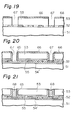
- FIGs 17 through 21 are diagrams showing the steps for producing lateral isolation of integrated circuits.
- a tantalum oxide layer (52) ca. 100 nm thick was deposited on a single crystalline silicon substrate (51) by reactive sputtering (Fig. 17) and was cut open in the desired region by means of photolithography and dry etching with a CHF 3 etchant so as to form lattice-like openings (52') (Fig. 18).
- a polycrystalline silicon layer (53) ca. 3 ⁇ m thick was deposited on the substrate (51) by chemical vapor deposition and was transformed by laser annealing into a single crystalline layer, since the surface of substrate .(51) contacting the polycrystalline silicon layer (53) acted as crystallizing nuclei.
- a silicon nitride layer (66) 100 nm thick was formed on the single crystalline silicon layer (53) by chemical vapor deposition. Windows 67 were opened through the silicon nitride layer (66) and the single crystalline silicon layer (53) by reactive ion etching with a CCl4 etchant (Fig. 19).
- the substrate was treated in wet oxygen at 1000°C for 80 minutes, and oxygen flowed through the windows (67) and diffused through the tantalum oxide layer (52) since the tantalum oxide acted as an oxygen passage. Consequently, not only the side wall (65) of the windows (67) but also the surface (54 1 ) of the silicon substrate (51) and the lower portion (55) of the transformed single crystalline silicon layer (53) were oxidized so as to form a silicon oxide insulating layer (Fig. 20).
- Silicon oxide layers (68) were deposited into the windows (67) by chemical vapor deposition so as to separate the single crystalline silicon islands (53), on which circuit elements could be produced.
- the silicon nitride layer (66) was removed with hot phosphoric acid.
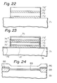
- Figures 22 and 23 are diagrams showing the steps for producing multilayered isolation of integrated circuits.
- a tantalum oxide layer (72) 50 nm thick and a polycrystalline silicon layer (73) were sequentially formed on a silicon substrate (71) in a manner similar to that of Example 4.
- Another tantalum oxide layer (72') and another polycrystalline silicon layer (73 1 ) were further formed thereon. Then these layers (72, 73, 72', 73') were patterned so as to expose the side surfaces of the tantalum oxide layers (72, 72 1 ) (Fig. 22).
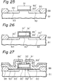
- Figures 24 through 29 are diagrams showing the steps for producing a 1(one)-transistor type nonvolatile memory device.
- Field oxide layers (88) and a tantalum oxide layer (89) 44 nm thick were produced on a p type silicon substrate (81) in a manner similar to that of Example 2. Then a polycrystalline silicon layer (86) 500 nm thick was formed on the tantalum oxide layer (89) by chemical vapor deposition (Fig. 24).
- N type source and drain regions (82, 83) were produced by masking with these layer (86', 89') and implanting arsenic as a donor type impurity into the substrate (81) (Fig. 25).
- the substrate was subjected to thermal oxidation in wet oxygen at 800°C for 10 minutes.
- the exposed silicon surfaces (90, 91) of the substrate and the gate electrode were oxidized.
- oxygen diffused through the tantalum oxide layer (89') so as to form the first and the third insulating layers of silicon oxide .(91', 90') under the gate electrode (86') (Fig. 26).
- the substrate was annealed in a mixture of nitrogen and 5% by volume of hydrogen at 1000°C for 20 minutes so as to reduce the tantalum oxide layer (89'). Consequently, a number of traps were produced due to the vacancy of oxygen in the reduced oxide layer (89"), which traps could accumulate electric charge (Fig. 27).
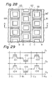
- Figure 28 is a plan of a 1-transistor type nonvolatile semiconductor random access memory device and indicates the following elements: field insulating oxide layers (88), gate electrodes (86'), contact holes (93) opened on the gate electrodes (86 1 ), an n type region (83) constituting bit lines defined by the adjacent dot-dash lines B, and an n type region (82) constituting earth lines defined by the adjacent broken lines C.
- field insulating oxide layers (88' in Fig. 27) and aluminum word lines (92 in Fig. 27) are not shown (Fig. 28).
- Fig. 29 shows an equivalent circuit of the random access memory shown in Fig. 28.
- Figure 29 illustrates bit lines B 1 , B2 and earth lines C 1 , C 2 connected to-drains and sources of each transistor, respectively, and word lines D 1 , D , D 3 connected to gates of each transistor. These constitute the memories 101 through 106.
- bit lines B 2 of cell 103 is maintained at an open potential so as to inhibit writing in cell 103 connected to the same word line as cell 101, and earth lines C 1 , C 2 are also maintained at an open potential so as to inhibit electron injection from the earth lines into cells 101 and 103.
- potentials +3 V and +5 V are applied to word line D 1 and bit line B 1 , respectively, and, then, it is determined whether the cell is ON or OFF, i.e., the absence of and the accumulation of electrons in the gate result in a current and no current between the source and drain, respectively.
- Bit line B 1 is connected to other cells 102, 104, 105.
- a potential +5 V is applied to word lines D 2 , D 3 .
- the effective electron discharge voltage is 5 V, which does not cause the tunnel effect.
- earth lines C 1 , C 2 on both sides of bit line B 1 are maintained at an open potential, thereby inhibiting current flow into the adjacent cells.
Landscapes
- Semiconductor Memories (AREA)
- Semiconductor Integrated Circuits (AREA)
- Formation Of Insulating Films (AREA)
Applications Claiming Priority (2)
| Application Number | Priority Date | Filing Date | Title |
|---|---|---|---|
| JP161281/81 | 1981-10-09 | ||
| JP56161281A JPH0722183B2 (ja) | 1981-10-09 | 1981-10-09 | 半導体装置用誘電体層の製造方法 |
Publications (3)
| Publication Number | Publication Date |
|---|---|
| EP0077200A2 true EP0077200A2 (fr) | 1983-04-20 |
| EP0077200A3 EP0077200A3 (en) | 1985-09-18 |
| EP0077200B1 EP0077200B1 (fr) | 1989-08-09 |
Family
ID=15732118
Family Applications (1)
| Application Number | Title | Priority Date | Filing Date |
|---|---|---|---|
| EP82305379A Expired EP0077200B1 (fr) | 1981-10-09 | 1982-10-08 | Procédé pour la formation de couches isolantes dans des dispositifs semiconducteurs |
Country Status (3)
| Country | Link |
|---|---|
| EP (1) | EP0077200B1 (fr) |
| JP (1) | JPH0722183B2 (fr) |
| DE (1) | DE3279873D1 (fr) |
Cited By (6)
| Publication number | Priority date | Publication date | Assignee | Title |
|---|---|---|---|---|
| FR2555365A1 (fr) * | 1983-11-22 | 1985-05-24 | Efcis | Procede de fabrication de circuit integre avec connexions de siliciure de tantale et circuit integre realise selon ce procede |
| EP0161619A3 (en) * | 1984-05-15 | 1989-05-31 | International Business Machines Corporation | Catalytic oxidation of solid materials |
| WO2002009167A3 (fr) * | 2000-07-20 | 2002-06-27 | Univ North Carolina State | Silicates metalliques a constante dielectrique elevee formes par reactions metal-surface maitrisees |
| US6642131B2 (en) * | 2001-06-21 | 2003-11-04 | Matsushita Electric Industrial Co., Ltd. | Method of forming a silicon-containing metal-oxide gate dielectric by depositing a high dielectric constant film on a silicon substrate and diffusing silicon from the substrate into the high dielectric constant film |
| WO2005010973A1 (fr) * | 2003-07-18 | 2005-02-03 | Forschungszentrum Jülich GmbH | Procede de reduction auto-ajustee de la taille de structures |
| CN111640866A (zh) * | 2020-07-16 | 2020-09-08 | 上海华力微电子有限公司 | 阻变存储器及其制备方法 |
Families Citing this family (7)
| Publication number | Priority date | Publication date | Assignee | Title |
|---|---|---|---|---|
| US5079191A (en) * | 1985-11-29 | 1992-01-07 | Hitachi, Ltd. | Process for producing a semiconductor device |
| JPS632363A (ja) * | 1986-06-20 | 1988-01-07 | Nec Corp | 容量膜 |
| JP2770856B2 (ja) * | 1987-08-20 | 1998-07-02 | 東京農工大学長 | 高誘電率酸化物薄膜の形成方法 |
| KR100319571B1 (ko) * | 1998-03-12 | 2002-01-09 | 루센트 테크놀러지스 인크 | 도프된 금속 산화물 유전물질들을 가진 전자 소자들과 도프된 금속 산화물 유전물질들을 가진 전자 소자들을 만드는 과정 |
| JP4590556B2 (ja) * | 2005-03-11 | 2010-12-01 | 国立大学法人 奈良先端科学技術大学院大学 | 半導体装置の製造方法 |
| JP4181195B2 (ja) * | 2006-09-14 | 2008-11-12 | 株式会社東芝 | 絶縁膜、およびそれを用いた半導体装置 |
| CN107424923A (zh) * | 2017-07-06 | 2017-12-01 | 鲁汶仪器有限公司(比利时) | 一种自限制精确刻蚀硅的方法 |
Family Cites Families (2)
| Publication number | Priority date | Publication date | Assignee | Title |
|---|---|---|---|---|
| DE1923279A1 (de) * | 1969-05-07 | 1970-12-23 | Licentia Gmbh | Transistor mit isolierter Steuerelektrode |
| JPS5745968A (en) * | 1980-08-29 | 1982-03-16 | Ibm | Capacitor with double dielectric unit |
-
1981
- 1981-10-09 JP JP56161281A patent/JPH0722183B2/ja not_active Expired - Lifetime
-
1982
- 1982-10-08 EP EP82305379A patent/EP0077200B1/fr not_active Expired
- 1982-10-08 DE DE8282305379T patent/DE3279873D1/de not_active Expired
Cited By (10)
| Publication number | Priority date | Publication date | Assignee | Title |
|---|---|---|---|---|
| FR2555365A1 (fr) * | 1983-11-22 | 1985-05-24 | Efcis | Procede de fabrication de circuit integre avec connexions de siliciure de tantale et circuit integre realise selon ce procede |
| EP0143700A3 (en) * | 1983-11-22 | 1985-09-18 | Societe Pour L'etude Et La Fabrication De Circuits Integres Speciaux - E.F.C.I.S. | Process for making integrated circuits having connectors comprising tantalum silicides, and integrated circuits made by this process |
| US4593454A (en) * | 1983-11-22 | 1986-06-10 | Societe pour d'Etude et la Fabrication de Circuits Integres Speciaux EFCS | Process for manufacturing an integrated circuit with tantalum silicide connections utilizing self-aligned oxidation |
| EP0161619A3 (en) * | 1984-05-15 | 1989-05-31 | International Business Machines Corporation | Catalytic oxidation of solid materials |
| WO2002009167A3 (fr) * | 2000-07-20 | 2002-06-27 | Univ North Carolina State | Silicates metalliques a constante dielectrique elevee formes par reactions metal-surface maitrisees |
| US6521911B2 (en) | 2000-07-20 | 2003-02-18 | North Carolina State University | High dielectric constant metal silicates formed by controlled metal-surface reactions |
| US6642131B2 (en) * | 2001-06-21 | 2003-11-04 | Matsushita Electric Industrial Co., Ltd. | Method of forming a silicon-containing metal-oxide gate dielectric by depositing a high dielectric constant film on a silicon substrate and diffusing silicon from the substrate into the high dielectric constant film |
| US7157780B2 (en) | 2001-06-21 | 2007-01-02 | Matsushita Electric Industrial Co., Ltd. | Semiconductor device and method for producing the same |
| WO2005010973A1 (fr) * | 2003-07-18 | 2005-02-03 | Forschungszentrum Jülich GmbH | Procede de reduction auto-ajustee de la taille de structures |
| CN111640866A (zh) * | 2020-07-16 | 2020-09-08 | 上海华力微电子有限公司 | 阻变存储器及其制备方法 |
Also Published As
| Publication number | Publication date |
|---|---|
| EP0077200A3 (en) | 1985-09-18 |
| EP0077200B1 (fr) | 1989-08-09 |
| JPH0722183B2 (ja) | 1995-03-08 |
| JPS5861634A (ja) | 1983-04-12 |
| DE3279873D1 (en) | 1989-09-14 |
Similar Documents
| Publication | Publication Date | Title |
|---|---|---|
| US4495219A (en) | Process for producing dielectric layers for semiconductor devices | |
| KR930001736B1 (ko) | 반도체장치의 제조방법 | |
| JPS6010773A (ja) | 1素子型fet−記憶キヤパシタ回路の形成方法 | |
| US7262101B2 (en) | Method of manufacturing a semiconductor integrated circuit device | |
| EP0077200A2 (fr) | Procédé pour la formation de couches isolantes dans des dispositifs semiconducteurs | |
| KR20000029395A (ko) | 양호한 전기적 특성과 높은 신뢰성을 갖는 반도체기억장치의 제조방법 | |
| US5518960A (en) | Method of manufacturing a wiring layer including amorphous silicon and refractory metal silicide | |
| JP2003168749A (ja) | 不揮発性半導体記憶装置及びその製造方法 | |
| CA1232365A (fr) | Structure double d'injection electronique a couche d'oxyde a auto-limitation | |
| EP0685883B1 (fr) | Procédé pour former un diélectrique amélioré pour un circuit intégré | |
| US4250206A (en) | Method of making non-volatile semiconductor memory elements | |
| US4288470A (en) | Method of making non-volatile semiconductor memory elements having multiple dielectric layers of silicon nitride, silicon dioxide, and rutile titanium dioxide | |
| US4735919A (en) | Method of making a floating gate memory cell | |
| JPH0311552B2 (fr) | ||
| EP0274390B1 (fr) | Dispositif de mémoire à semi-conducteur et son procédé de fabrication | |
| US5149666A (en) | Method of manufacturing a semiconductor memory device having a floating gate electrode composed of 2-10 silicon grains | |
| US4683640A (en) | Method of making a floating gate memory cell | |
| JPS63237456A (ja) | 半導体装置 | |
| JP2632839B2 (ja) | 集積回路の製造方法 | |
| KR100279052B1 (ko) | 강유전체게이트를가지는전계효과트랜지스터를이용한불휘발성기억소자및그제조방법 | |
| JPH0736438B2 (ja) | 半導体装置 | |
| JPS62219659A (ja) | Mos型半導体記憶装置 | |
| JPH0381297B2 (fr) | ||
| KR950003225B1 (ko) | 절연막의 제조 방법 | |
| US6730607B2 (en) | Method for fabricating a barrier layer |
Legal Events
| Date | Code | Title | Description |
|---|---|---|---|
| PUAI | Public reference made under article 153(3) epc to a published international application that has entered the european phase |
Free format text: ORIGINAL CODE: 0009012 |
|
| AK | Designated contracting states |
Designated state(s): DE FR GB |
|
| PUAL | Search report despatched |
Free format text: ORIGINAL CODE: 0009013 |
|
| AK | Designated contracting states |
Designated state(s): DE FR GB |
|
| 17P | Request for examination filed |
Effective date: 19851118 |
|
| 17Q | First examination report despatched |
Effective date: 19870924 |
|
| GRAA | (expected) grant |
Free format text: ORIGINAL CODE: 0009210 |
|
| AK | Designated contracting states |
Kind code of ref document: B1 Designated state(s): DE FR GB |
|
| REF | Corresponds to: |
Ref document number: 3279873 Country of ref document: DE Date of ref document: 19890914 |
|
| ET | Fr: translation filed | ||
| PLBE | No opposition filed within time limit |
Free format text: ORIGINAL CODE: 0009261 |
|
| STAA | Information on the status of an ep patent application or granted ep patent |
Free format text: STATUS: NO OPPOSITION FILED WITHIN TIME LIMIT |
|
| 26N | No opposition filed | ||
| PGFP | Annual fee paid to national office [announced via postgrant information from national office to epo] |
Ref country code: FR Payment date: 19931028 Year of fee payment: 12 |
|
| PG25 | Lapsed in a contracting state [announced via postgrant information from national office to epo] |
Ref country code: FR Effective date: 19950630 |
|
| REG | Reference to a national code |
Ref country code: FR Ref legal event code: ST |
|
| PGFP | Annual fee paid to national office [announced via postgrant information from national office to epo] |
Ref country code: GB Payment date: 19950929 Year of fee payment: 14 |
|
| PGFP | Annual fee paid to national office [announced via postgrant information from national office to epo] |
Ref country code: DE Payment date: 19951012 Year of fee payment: 14 |
|
| PG25 | Lapsed in a contracting state [announced via postgrant information from national office to epo] |
Ref country code: GB Effective date: 19961008 |
|
| GBPC | Gb: european patent ceased through non-payment of renewal fee |
Effective date: 19961008 |
|
| PG25 | Lapsed in a contracting state [announced via postgrant information from national office to epo] |
Ref country code: DE Effective date: 19970701 |