EP0078220A2 - Interférences de silicium polycristallin pour transistors bipolaires en circuit flip-flop - Google Patents
Interférences de silicium polycristallin pour transistors bipolaires en circuit flip-flop Download PDFInfo
- Publication number
- EP0078220A2 EP0078220A2 EP82401970A EP82401970A EP0078220A2 EP 0078220 A2 EP0078220 A2 EP 0078220A2 EP 82401970 A EP82401970 A EP 82401970A EP 82401970 A EP82401970 A EP 82401970A EP 0078220 A2 EP0078220 A2 EP 0078220A2
- Authority
- EP
- European Patent Office
- Prior art keywords
- layer
- conductivity type
- substrate
- polycrystalline silicon
- region
- Prior art date
- Legal status (The legal status is an assumption and is not a legal conclusion. Google has not performed a legal analysis and makes no representation as to the accuracy of the status listed.)
- Granted
Links
Images


Classifications
-
- H—ELECTRICITY
- H10—SEMICONDUCTOR DEVICES; ELECTRIC SOLID-STATE DEVICES NOT OTHERWISE PROVIDED FOR
- H10W—GENERIC PACKAGES, INTERCONNECTIONS, CONNECTORS OR OTHER CONSTRUCTIONAL DETAILS OF DEVICES COVERED BY CLASS H10
- H10W20/00—Interconnections in chips, wafers or substrates
- H10W20/40—Interconnections external to wafers or substrates, e.g. back-end-of-line [BEOL] metallisations or vias connecting to gate electrodes
- H10W20/41—Interconnections external to wafers or substrates, e.g. back-end-of-line [BEOL] metallisations or vias connecting to gate electrodes characterised by their conductive parts
- H10W20/44—Conductive materials thereof
- H10W20/4451—Semiconductor materials, e.g. polysilicon
-
- H—ELECTRICITY
- H10—SEMICONDUCTOR DEVICES; ELECTRIC SOLID-STATE DEVICES NOT OTHERWISE PROVIDED FOR
- H10P—GENERIC PROCESSES OR APPARATUS FOR THE MANUFACTURE OR TREATMENT OF DEVICES COVERED BY CLASS H10
- H10P32/00—Diffusion of dopants within, into or out of wafers, substrates or parts of devices
- H10P32/10—Diffusion of dopants within, into or out of semiconductor bodies or layers
- H10P32/14—Diffusion of dopants within, into or out of semiconductor bodies or layers within a single semiconductor body or layer in a solid phase; between different semiconductor bodies or layers, both in a solid phase
- H10P32/1408—Diffusion of dopants within, into or out of semiconductor bodies or layers within a single semiconductor body or layer in a solid phase; between different semiconductor bodies or layers, both in a solid phase from or through or into an external applied layer, e.g. photoresist or nitride layers
- H10P32/1414—Diffusion of dopants within, into or out of semiconductor bodies or layers within a single semiconductor body or layer in a solid phase; between different semiconductor bodies or layers, both in a solid phase from or through or into an external applied layer, e.g. photoresist or nitride layers the applied layer being silicon, silicide or SIPOS, e.g. polysilicon or porous silicon
-
- H—ELECTRICITY
- H10—SEMICONDUCTOR DEVICES; ELECTRIC SOLID-STATE DEVICES NOT OTHERWISE PROVIDED FOR
- H10P—GENERIC PROCESSES OR APPARATUS FOR THE MANUFACTURE OR TREATMENT OF DEVICES COVERED BY CLASS H10
- H10P32/00—Diffusion of dopants within, into or out of wafers, substrates or parts of devices
- H10P32/10—Diffusion of dopants within, into or out of semiconductor bodies or layers
- H10P32/17—Diffusion of dopants within, into or out of semiconductor bodies or layers characterised by the semiconductor material
- H10P32/171—Diffusion of dopants within, into or out of semiconductor bodies or layers characterised by the semiconductor material being group IV material
-
- H—ELECTRICITY
- H10—SEMICONDUCTOR DEVICES; ELECTRIC SOLID-STATE DEVICES NOT OTHERWISE PROVIDED FOR
- H10W—GENERIC PACKAGES, INTERCONNECTIONS, CONNECTORS OR OTHER CONSTRUCTIONAL DETAILS OF DEVICES COVERED BY CLASS H10
- H10W20/00—Interconnections in chips, wafers or substrates
- H10W20/01—Manufacture or treatment
- H10W20/031—Manufacture or treatment of conductive parts of the interconnections
- H10W20/064—Manufacture or treatment of conductive parts of the interconnections by modifying the conductivity of conductive parts, e.g. by alloying
- H10W20/066—Manufacture or treatment of conductive parts of the interconnections by modifying the conductivity of conductive parts, e.g. by alloying by forming silicides of refractory metals
Definitions
- This invention relates to integrated circuits and methods of manufacturing them, and in particular to an unusually compact bipolar transistor flip-flop structure having polycrystalline silicon interconnections, and a method of fabricating it.
- a method of fabricating electrically connected regions of opposite conductivity in a substrate comprising: depositing a layer of semiconductor material on the substrate, a first portion of the layer being first conductivity type, and a second portion of the layer being opposite conductivity type; depositing a layer of electrically conductive material over the layer of semiconductor material: and transferring some of the first conductivity type impurity and some of the opposite conductivity type impurity from the layer of semiconductor material into the substrate to thereby create electrically connected regions of opposite conductivity in the substrate.
- Another aspect of the invention includes an integrated circuit structure comprising: a semiconductor substrate having a surface; first and second transistor structures, each having a first region of first conductivity type and a second region of opposite conductivity type adjacent the surface of the substrate; first and second connections of semiconductor material disposed on the surface of the substrate, each extending between a first conductivity type region in one of the first and second transistors and an opposite conductivity type region in the other of the first and second transistors, separate portions of each of the first and second connections being of conductivity type to correspond to the conductivity type of the first or second region beneath the connection; and a layer of electrically conductive material disposed on each of the first and second connections to electrically connect the separate portions of the connection.
- substrate refers to an underlying structure of arbitrary complexity. Used in this manner a substrate may contain numerous passive and/or active electronic components. For example, used in this sense, in Figure 2 layer 21 is disposed on a "substrate.” Another sense in which substrate is used in this application is to refer only to the monocrystallin: undoped silicon wafer used as a starting point for the fabrication of an integrated circuit. In this manner in Figure 2 region 10 is termed a "substrate.” The context in which the word appears will indicate the intended meaning.
- Figure 1 illustrates a cross-sectional view of a semiconductor structure including a P conductivity type silicon substrate 10, an N conductivity type buried layer 12, intrinsic epitaxial silicon layer 15, and silicon dioxide insulation 16.
- substrate 10 will have a resistivity of 2 ohm- centimeters while buried layer 12 will be doped with N conductivity type impurities to a concentration of 10 19 atoms per cubic centimeter.
- the structure shown in Figure 1 may be fabricated using well-known semiconductor fabrication techniques, for example, as taught by Douglas Peltzer in United states Patent Nc. 3,648,125 entitled "Method of Fabricating Integrated circuits With Oxidized Isolation and the Resulting Structure.”
- epitaxial layer 15 is then doped with a suitable P conductivity type impurity, such as boron, to a concentration of 5x10 16 atoms per cubic centimeter.
- a suitable P conductivity type impurity such as boron
- the lightly doped P type region 15 will serve as the intrinsic base for subsequently formed NPN transistors.
- Layer 15 may be most readily doped by implanting boron ions into the epitaxial layer using a dose of 10 13 atoms per square centimeter and an implant energy of 150 kev.
- a layer of polycrystalline silicon 21 approximately 5000 Angstroms thick is deposited across the upper surface of the structure, for example, using chemical vapor deposition.
- the polycrystalline silicon 21 is then masked using well-known techniques and N and P conductivity type impurities introduced as depicted in Figure 2.
- the N type portion 23 of layer 21 will be doped to a concentration of approximately 10 20 atoms per cubic centimeter of arsenic, while the P type portion 25 of layer 21 will be doped with approximately 10 19 atoms per cubic centimeter of boron.
- the precise location of the junction 26 between regions 23 and 25 is not critical because this junction is later removed (see Figure 3).
- only those portions of layer 21 which are not subsequently removed need be doped.
- only two portions 32 and 34 of layer 21 remain after subsequent process steps and these are the only portions of layer 21 which need be doped.
- regions 23 and 25 are doped, other portions of layer 21 in front of the cross-section shown in Figure 2 are also doped. These regions 32' and 34' are shown most clearly in Figure 6. As shown there, region 32' will be doped with an opposite conductivity type to region 32 and region 34' will be doped with opposite conductivity to region 34. The function of opposite conductivity type regions 32' and 34' is discussed in conjunction with Figure 5.
- silicide layer 29 comprises a refractory metal silicide, such as tantalum silicide or tungsten silicide, approximately 1000 Angstroms thick which is fabricated by chemical vapor deposition
- a layer of silicon dioxide 30 approximately 3000 Angstroms thick is fabricated by heating silicide 29 to a temperature of 800°C for 3 hours in a steam ambient.
- silicide 29 will be used to "short" P-N junctions created in polycrystalline silicon 25.
- Oxide 30 will protect silicide 29 from subsequent processing steps which are described in conjunction with Figures 3 and 4.
- the structure in Figure 2 is then masked and etched using known photolithographic and chemical or plasma etching techniques to define strips (extending into and out of the illustration) of polycrystalline silicon 23 and 25 together with overlying silicide 29 and 29' and silicon dioxide 30.
- the strips 32 and 34 may be etched using any desired technique, for example with a plasma which comprises carbon tetrafluoride to etch oxide 30, and carbon tetrachloride to etch silicide 29 and polycrystalline silicon 23 and 25.
- the resulting integrated circuit structure is heated to a temperature of 1000° C for 60 minutes in steam.
- a layer of silicon dioxide 36 will be formed across the surface of epitaxial layer 15 and on the sides of strips 32 and 34.
- the silicon dioxide 30 on the upper surface of the strips 32 and 34 will become thicker.
- a thicker layer of silicon dioxide 36b will form on the sides of strips 32 and 34 than layer 36a on the surface of epitaxial layer 15.
- layer 36b will be approximately 1500 Angstroms thick while layer 36a will be approximately 500 Angstroms thick.
- the structure shown in Figure 3 is then etched in a well-known manner, for example, with a plasma containing carbon tetrafluoride and hydrogen to remove the thin oxide 36a on the surface of epitaxial layer 15. Because of the different thicknesses of layers 36a and 36b some of layer 36b will remain on the sides of polycrystalline silicon regions 23 and 25 after all of layer 36a is removed. The oxide 36b which remains on the sides of the polycrystalline silicon regions 23 and 25 and oxide 30 on top silicide 29 and 29' will electrically isolate these regions from subsequently formed layers overlying the strips 32 and 34.
- a relatively thick layer of polycrystalline silicon 39 is then deposited across the upper surface of the structure.
- layer 39 is doped with P conductivity type impurity, for example, boron, to an impurity concentration of 10 19 atoms per cubic centimeter.
- Polycrystalline silicon layer 39 may be fabricated using chemical vapor deposition and doped at the same time it is deposited. Using well-known photolithographic techniques, polycrystalline slicon 39 is masked and defined, for example, by plasma etching. In the preferred embodiment polycrystalline silicon 39 completely covers all of epitaxial silicon 15 except where polycrystalline silicon regions 23 and 25 and silicon dioxide 36 overlie layer 15.
- N type region 42 comprises the collector of an inverted NPN transistor having emitter 12 and base 15. The P conductivity type dopant in the upper portions of epitaxial silicon 15 outside of collector 42 lowers the resistance of the P type base 15.
- Figure 5 is a cross-section taken at right angles with respect to Figure 4.
- Figure 6 a top view of the completed structure, shows the relationship of Figures 4 and 5.
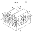
- Figure 7 shows the completed structure prior to formation of any desired passivating layers or electrical connections.
- dashed line 60 designates the outer boundary of a first epitaxial silicon pocket surrounded by silicon dioxide 16.
- dashed line 62 designates the boundary of a second such pocket.
- a first transistor is formed in region 60 (and shown in Figure 4), while a similar second transistor structure is formed within region 62.
- the strips are designated 32 and 34 at the end shown in cross-section in Figure 4, and 32' and 34' at the opposite end.
- the polycrystalline silicon 23 or 25 underlying the silicide 29 or 29' at that end 32' and 34' of each strip is of opposite conductivity to the polycrystalline silicon 23 or 25 at the other end 32 or 34 of the strip.
- the opposite conductivity type polycrystalline silicon 25' is shown more clearly in Figure 5.
- Metal silicide 29 short circuits P-N junction 63 by electrically connecting N type region 23 to P type region 23'; and silicide 29' short circuits P-N junction 64 by electrically connecting P type region 25 toN type region 25'.
- Polycrystalline silicon 25' is electrically connected to, and was the source of dopant for, the collector 42' of the transistor formed in region 62 of epitaxial layer 15, while buried layer 12 and epitaxial layer 15 function as emitter and base, respectively.
- Polycrystalline silicon 25 is electrically connected to the base 15 via the P type region 45 in the first transistor, which is formed within region 60 of the epitaxial layer 15.
- region 23 connects to the N type collector 42 of the first transistor, while P type polycrystalline silicon 23' (not shown) connects to the base of the second transistor.
- Polycrystalline layers 39 and 50 reduce the base resistances of the respective two transistors.
- Figure 8 is an electrical schematic showing the equivalent discrete circuit fabricated by the integrated circuit structure shown in Figures 4-7.
- Figure 8 illustrates the electrical paths between various components. shown in Figures 4-7.
- the N type collector 42 of the first transistor Q1 is connected to N type polycrystalline silicon region 23, which is connected by metal silicide layer 29 to P type polycrystalline silicon region 23', and in turn to the base 15' of the second transistor Q2.
- collector 42' of the second transistor Q2 is connected to N type polycrystalline silicon 25', metal silicide layer 29', P type polycrystalline silicon 25, base contact 45, and finally to base 15 of the first transistor Ql.
- Buried layer 12 provides the commonly coupled emitters of both the first and second transistors Ql and Q2.
- the structure of the bipolar transistor flip-flop of this invention together with the method of manufacturing it, enable the creation of a very compact flip-flop.
- the flip-flop may be fabricated in about 100 square micrometers, thereby enabling fabrication of more than a quarter million such flip-flops on a die 200 mils square.
Landscapes
- Bipolar Transistors (AREA)
- Bipolar Integrated Circuits (AREA)
Applications Claiming Priority (2)
| Application Number | Priority Date | Filing Date | Title |
|---|---|---|---|
| US315553 | 1981-10-27 | ||
| US06/315,553 US4617071A (en) | 1981-10-27 | 1981-10-27 | Method of fabricating electrically connected regions of opposite conductivity type in a semiconductor structure |
Publications (3)
| Publication Number | Publication Date |
|---|---|
| EP0078220A2 true EP0078220A2 (fr) | 1983-05-04 |
| EP0078220A3 EP0078220A3 (en) | 1984-12-27 |
| EP0078220B1 EP0078220B1 (fr) | 1987-09-09 |
Family
ID=23224958
Family Applications (1)
| Application Number | Title | Priority Date | Filing Date |
|---|---|---|---|
| EP82401970A Expired EP0078220B1 (fr) | 1981-10-27 | 1982-10-26 | Interférences de silicium polycristallin pour transistors bipolaires en circuit flip-flop |
Country Status (5)
| Country | Link |
|---|---|
| US (1) | US4617071A (fr) |
| EP (1) | EP0078220B1 (fr) |
| JP (2) | JPS5886761A (fr) |
| CA (1) | CA1203920A (fr) |
| DE (1) | DE3277266D1 (fr) |
Cited By (4)
| Publication number | Priority date | Publication date | Assignee | Title |
|---|---|---|---|---|
| EP0145036A1 (fr) * | 1983-09-15 | 1985-06-19 | Koninklijke Philips Electronics N.V. | Dispositif semi-conducteur ayant une structure d'interconnexion |
| GB2153146A (en) * | 1984-01-10 | 1985-08-14 | Ates Componenti Elettron | Improvements in or relating to manufacture of cmos transistors |
| DE19825612A1 (de) * | 1998-06-08 | 1999-12-16 | Siemens Ag | Halbleiterbauelement mit einer Polysiliziumverdrahtung und Verfahren zu dessen Herstellung |
| US7375086B2 (en) | 2000-10-30 | 2008-05-20 | The Regents Of The University Of Michigan | Modulators of Nod2 signaling |
Families Citing this family (8)
| Publication number | Priority date | Publication date | Assignee | Title |
|---|---|---|---|---|
| NL8105920A (nl) * | 1981-12-31 | 1983-07-18 | Philips Nv | Halfgeleiderinrichting en werkwijze voor het vervaardigen van een dergelijke halfgeleiderinrichting. |
| JPS60137061A (ja) * | 1983-12-26 | 1985-07-20 | Matsushita Electric Ind Co Ltd | 半導体集積回路装置及びその製造方法 |
| US5151387A (en) * | 1990-04-30 | 1992-09-29 | Sgs-Thomson Microelectronics, Inc. | Polycrystalline silicon contact structure |
| US5289024A (en) * | 1990-08-07 | 1994-02-22 | National Semiconductor Corporation | Bipolar transistor with diffusion compensation |
| US5539233A (en) * | 1993-07-22 | 1996-07-23 | Texas Instruments Incorporated | Controlled low collector breakdown voltage vertical transistor for ESD protection circuits |
| US6087214A (en) * | 1998-04-29 | 2000-07-11 | Vlsi Technology, Inc. | Arrangement and method for DRAM cell using shallow trench isolation |
| US7745301B2 (en) | 2005-08-22 | 2010-06-29 | Terapede, Llc | Methods and apparatus for high-density chip connectivity |
| US8957511B2 (en) | 2005-08-22 | 2015-02-17 | Madhukar B. Vora | Apparatus and methods for high-density chip connectivity |
Family Cites Families (10)
| Publication number | Priority date | Publication date | Assignee | Title |
|---|---|---|---|---|
| US3648125A (en) * | 1971-02-02 | 1972-03-07 | Fairchild Camera Instr Co | Method of fabricating integrated circuits with oxidized isolation and the resulting structure |
| JPS5147592B2 (fr) * | 1972-12-19 | 1976-12-15 | ||
| JPS554965A (en) * | 1978-06-27 | 1980-01-14 | Toshiba Corp | Semiconductor |
| CA1142261A (fr) * | 1979-06-29 | 1983-03-01 | Siegfried K. Wiedmann | Methode d'interconnexion de regions semiconductrices de types opposes |
| JPS5662339A (en) * | 1979-10-26 | 1981-05-28 | Chiyou Lsi Gijutsu Kenkyu Kumiai | Production of semiconductor device |
| US4322882A (en) * | 1980-02-04 | 1982-04-06 | Fairchild Camera & Instrument Corp. | Method for making an integrated injection logic structure including a self-aligned base contact |
| US4512075A (en) * | 1980-08-04 | 1985-04-23 | Fairchild Camera & Instrument Corporation | Method of making an integrated injection logic cell having self-aligned collector and base reduced resistance utilizing selective diffusion from polycrystalline regions |
| US4398338A (en) * | 1980-12-24 | 1983-08-16 | Fairchild Camera & Instrument Corp. | Fabrication of high speed, nonvolatile, electrically erasable memory cell and system utilizing selective masking, deposition and etching techniques |
| US4418468A (en) * | 1981-05-08 | 1983-12-06 | Fairchild Camera & Instrument Corporation | Process for fabricating a logic structure utilizing polycrystalline silicon Schottky diodes |
| US4488350A (en) * | 1981-10-27 | 1984-12-18 | Fairchild Camera & Instrument Corp. | Method of making an integrated circuit bipolar memory cell |
-
1981
- 1981-10-27 US US06/315,553 patent/US4617071A/en not_active Expired - Lifetime
-
1982
- 1982-10-26 DE DE8282401970T patent/DE3277266D1/de not_active Expired
- 1982-10-26 CA CA000414200A patent/CA1203920A/fr not_active Expired
- 1982-10-26 EP EP82401970A patent/EP0078220B1/fr not_active Expired
- 1982-10-27 JP JP57187638A patent/JPS5886761A/ja active Pending
-
1992
- 1992-09-21 JP JP4251456A patent/JPH0645537A/ja active Pending
Cited By (6)
| Publication number | Priority date | Publication date | Assignee | Title |
|---|---|---|---|---|
| EP0145036A1 (fr) * | 1983-09-15 | 1985-06-19 | Koninklijke Philips Electronics N.V. | Dispositif semi-conducteur ayant une structure d'interconnexion |
| GB2153146A (en) * | 1984-01-10 | 1985-08-14 | Ates Componenti Elettron | Improvements in or relating to manufacture of cmos transistors |
| DE19825612A1 (de) * | 1998-06-08 | 1999-12-16 | Siemens Ag | Halbleiterbauelement mit einer Polysiliziumverdrahtung und Verfahren zu dessen Herstellung |
| US6429520B1 (en) | 1998-06-08 | 2002-08-06 | Siemens Aktiengesellschaft | Semiconductor component with silicon wiring and method of fabricating the component |
| DE19825612C2 (de) * | 1998-06-08 | 2002-10-31 | Infineon Technologies Ag | Halbleiterbauelement mit einer Polysiliziumverdrahtung und Verfahren zu dessen Herstellung |
| US7375086B2 (en) | 2000-10-30 | 2008-05-20 | The Regents Of The University Of Michigan | Modulators of Nod2 signaling |
Also Published As
| Publication number | Publication date |
|---|---|
| EP0078220A3 (en) | 1984-12-27 |
| JPH0645537A (ja) | 1994-02-18 |
| CA1203920A (fr) | 1986-04-29 |
| DE3277266D1 (en) | 1987-10-15 |
| US4617071A (en) | 1986-10-14 |
| EP0078220B1 (fr) | 1987-09-09 |
| JPS5886761A (ja) | 1983-05-24 |
Similar Documents
| Publication | Publication Date | Title |
|---|---|---|
| US4543595A (en) | Bipolar memory cell | |
| CA1241770A (fr) | Methode de fabrication de regions auto-alignees en siliciure de metal pour circuits integres a electrodes auto-alignees en silicium polycristallin | |
| US4299024A (en) | Fabrication of complementary bipolar transistors and CMOS devices with poly gates | |
| US4418468A (en) | Process for fabricating a logic structure utilizing polycrystalline silicon Schottky diodes | |
| EP0083816B1 (fr) | Dispositif semi-conducteur comprenant une configuration d'interconnexion | |
| EP0021403B1 (fr) | Circuits semiconducteurs autoalignés | |
| US5670820A (en) | Semiconductor element incorporating a resistive device | |
| JPS62588B2 (fr) | ||
| US4425379A (en) | Polycrystalline silicon Schottky diode array | |
| EP0084500B1 (fr) | Cellules mémoire pour RAM de haute densité réalisées par implantation ionique | |
| EP0080730B1 (fr) | Dispositif semi-conducteur comprenant des couches conductrices et procédé pour le fabriquer | |
| EP0078220B1 (fr) | Interférences de silicium polycristallin pour transistors bipolaires en circuit flip-flop | |
| US5019532A (en) | Method for forming a fuse and fuse made thereby | |
| US4673969A (en) | Semiconductor device having multiple conductive layers and the method of manufacturing the semiconductor device | |
| CA1148667A (fr) | Methode de fabrication de circuits logiques integres a injection comprenant un contact de base auto-aligne | |
| EP0030147B1 (fr) | Procédé de fabrication d'un circuit intégré à semi-conducteur | |
| US4584594A (en) | Logic structure utilizing polycrystalline silicon Schottky diodes | |
| US4628339A (en) | Polycrystalline silicon Schottky diode array | |
| US4883772A (en) | Process for making a self-aligned silicide shunt | |
| US5146307A (en) | Fuse having a dielectric layer between sloped insulator sidewalls | |
| US4624863A (en) | Method of fabricating Schottky diodes and electrical interconnections in semiconductor structures | |
| US7101750B2 (en) | Semiconductor device for integrated injection logic cell and process for fabricating the same | |
| EP0264309B1 (fr) | Shunt de base auto-aligné pour un transistor | |
| EP0078221A2 (fr) | Diode en silicium polycristallin à contact en siliciure métallique | |
| EP0145036B1 (fr) | Dispositif semi-conducteur ayant une structure d'interconnexion |
Legal Events
| Date | Code | Title | Description |
|---|---|---|---|
| PUAI | Public reference made under article 153(3) epc to a published international application that has entered the european phase |
Free format text: ORIGINAL CODE: 0009012 |
|
| AK | Designated contracting states |
Designated state(s): DE FR GB IT NL |
|
| PUAL | Search report despatched |
Free format text: ORIGINAL CODE: 0009013 |
|
| AK | Designated contracting states |
Designated state(s): DE FR GB IT NL |
|
| 17P | Request for examination filed |
Effective date: 19850524 |
|
| 17Q | First examination report despatched |
Effective date: 19861202 |
|
| GRAA | (expected) grant |
Free format text: ORIGINAL CODE: 0009210 |
|
| ITF | It: translation for a ep patent filed | ||
| AK | Designated contracting states |
Kind code of ref document: B1 Designated state(s): DE FR GB IT NL |
|
| REF | Corresponds to: |
Ref document number: 3277266 Country of ref document: DE Date of ref document: 19871015 |
|
| ET | Fr: translation filed | ||
| PLBE | No opposition filed within time limit |
Free format text: ORIGINAL CODE: 0009261 |
|
| STAA | Information on the status of an ep patent application or granted ep patent |
Free format text: STATUS: NO OPPOSITION FILED WITHIN TIME LIMIT |
|
| 26N | No opposition filed | ||
| ITTA | It: last paid annual fee | ||
| PGFP | Annual fee paid to national office [announced via postgrant information from national office to epo] |
Ref country code: GB Payment date: 19940927 Year of fee payment: 13 |
|
| PGFP | Annual fee paid to national office [announced via postgrant information from national office to epo] |
Ref country code: FR Payment date: 19941012 Year of fee payment: 13 |
|
| PGFP | Annual fee paid to national office [announced via postgrant information from national office to epo] |
Ref country code: NL Payment date: 19941031 Year of fee payment: 13 |
|
| PG25 | Lapsed in a contracting state [announced via postgrant information from national office to epo] |
Ref country code: GB Effective date: 19951026 |
|
| PG25 | Lapsed in a contracting state [announced via postgrant information from national office to epo] |
Ref country code: NL Effective date: 19960501 |
|
| GBPC | Gb: european patent ceased through non-payment of renewal fee |
Effective date: 19951026 |
|
| PG25 | Lapsed in a contracting state [announced via postgrant information from national office to epo] |
Ref country code: FR Effective date: 19960628 |
|
| NLV4 | Nl: lapsed or anulled due to non-payment of the annual fee |
Effective date: 19960501 |
|
| REG | Reference to a national code |
Ref country code: FR Ref legal event code: ST |
|
| PGFP | Annual fee paid to national office [announced via postgrant information from national office to epo] |
Ref country code: DE Payment date: 20011004 Year of fee payment: 20 |