EP0080652A2 - Phototransistor MOS en technologie à film mince, son procédé de fabrication et sa méthode d'utilisation - Google Patents
Phototransistor MOS en technologie à film mince, son procédé de fabrication et sa méthode d'utilisation Download PDFInfo
- Publication number
- EP0080652A2 EP0080652A2 EP82110602A EP82110602A EP0080652A2 EP 0080652 A2 EP0080652 A2 EP 0080652A2 EP 82110602 A EP82110602 A EP 82110602A EP 82110602 A EP82110602 A EP 82110602A EP 0080652 A2 EP0080652 A2 EP 0080652A2
- Authority
- EP
- European Patent Office
- Prior art keywords
- layer
- polycrystalline silicon
- source
- silicon
- semiconductor body
- Prior art date
- Legal status (The legal status is an assumption and is not a legal conclusion. Google has not performed a legal analysis and makes no representation as to the accuracy of the status listed.)
- Granted
Links
- 238000004519 manufacturing process Methods 0.000 title claims abstract description 8
- 239000010409 thin film Substances 0.000 title claims abstract description 7
- 238000005516 engineering process Methods 0.000 title claims abstract description 6
- 238000000034 method Methods 0.000 title claims description 7
- 229910021420 polycrystalline silicon Inorganic materials 0.000 claims abstract description 25
- 239000004065 semiconductor Substances 0.000 claims abstract description 19
- 230000003647 oxidation Effects 0.000 claims abstract description 11
- 238000007254 oxidation reaction Methods 0.000 claims abstract description 11
- 238000000151 deposition Methods 0.000 claims description 10
- 239000000758 substrate Substances 0.000 claims description 10
- 238000002161 passivation Methods 0.000 claims description 9
- 229910004298 SiO 2 Inorganic materials 0.000 claims description 8
- XUIMIQQOPSSXEZ-UHFFFAOYSA-N Silicon Chemical compound [Si] XUIMIQQOPSSXEZ-UHFFFAOYSA-N 0.000 claims description 8
- 230000008021 deposition Effects 0.000 claims description 8
- 229910052710 silicon Inorganic materials 0.000 claims description 8
- 229910021417 amorphous silicon Inorganic materials 0.000 claims description 7
- 229910052581 Si3N4 Inorganic materials 0.000 claims description 6
- 239000010703 silicon Substances 0.000 claims description 6
- HQVNEWCFYHHQES-UHFFFAOYSA-N silicon nitride Chemical compound N12[Si]34N5[Si]62N3[Si]51N64 HQVNEWCFYHHQES-UHFFFAOYSA-N 0.000 claims description 6
- 239000012808 vapor phase Substances 0.000 claims description 6
- 229910052785 arsenic Inorganic materials 0.000 claims description 5
- 238000009792 diffusion process Methods 0.000 claims description 5
- 238000005468 ion implantation Methods 0.000 claims description 5
- 239000000463 material Substances 0.000 claims description 4
- UFHFLCQGNIYNRP-UHFFFAOYSA-N Hydrogen Chemical compound [H][H] UFHFLCQGNIYNRP-UHFFFAOYSA-N 0.000 claims description 3
- BLRPTPMANUNPDV-UHFFFAOYSA-N Silane Chemical group [SiH4] BLRPTPMANUNPDV-UHFFFAOYSA-N 0.000 claims description 3
- -1 arsenic ions Chemical class 0.000 claims description 3
- 229910052739 hydrogen Inorganic materials 0.000 claims description 3
- 239000001257 hydrogen Substances 0.000 claims description 3
- 229910000077 silane Inorganic materials 0.000 claims description 3
- 238000005979 thermal decomposition reaction Methods 0.000 claims description 3
- RQNWIZPPADIBDY-UHFFFAOYSA-N arsenic atom Chemical compound [As] RQNWIZPPADIBDY-UHFFFAOYSA-N 0.000 claims description 2
- 239000010410 layer Substances 0.000 claims 23
- 229910021419 crystalline silicon Inorganic materials 0.000 claims 2
- 239000011241 protective layer Substances 0.000 claims 2
- 239000002019 doping agent Substances 0.000 claims 1
- 229910052751 metal Inorganic materials 0.000 claims 1
- 239000002184 metal Substances 0.000 claims 1
- 238000007740 vapor deposition Methods 0.000 claims 1
- 230000007547 defect Effects 0.000 description 6
- WUPHOULIZUERAE-UHFFFAOYSA-N 3-(oxolan-2-yl)propanoic acid Chemical compound OC(=O)CCC1CCCO1 WUPHOULIZUERAE-UHFFFAOYSA-N 0.000 description 3
- 229910052980 cadmium sulfide Inorganic materials 0.000 description 3
- 230000000694 effects Effects 0.000 description 2
- 238000009413 insulation Methods 0.000 description 2
- LIVNPJMFVYWSIS-UHFFFAOYSA-N silicon monoxide Chemical compound [Si-]#[O+] LIVNPJMFVYWSIS-UHFFFAOYSA-N 0.000 description 2
- 238000000137 annealing Methods 0.000 description 1
- 230000004888 barrier function Effects 0.000 description 1
- WUKWITHWXAAZEY-UHFFFAOYSA-L calcium difluoride Chemical compound [F-].[F-].[Ca+2] WUKWITHWXAAZEY-UHFFFAOYSA-L 0.000 description 1
- 229910001634 calcium fluoride Inorganic materials 0.000 description 1
- 239000000969 carrier Substances 0.000 description 1
- 238000006243 chemical reaction Methods 0.000 description 1
- 238000005229 chemical vapour deposition Methods 0.000 description 1
- 238000010276 construction Methods 0.000 description 1
- 238000002347 injection Methods 0.000 description 1
- 239000007924 injection Substances 0.000 description 1
- 229910021421 monocrystalline silicon Inorganic materials 0.000 description 1
- 238000011017 operating method Methods 0.000 description 1
- 231100000289 photo-effect Toxicity 0.000 description 1
- 230000001681 protective effect Effects 0.000 description 1
Images
Classifications
-
- H—ELECTRICITY
- H10—SEMICONDUCTOR DEVICES; ELECTRIC SOLID-STATE DEVICES NOT OTHERWISE PROVIDED FOR
- H10D—INORGANIC ELECTRIC SEMICONDUCTOR DEVICES
- H10D62/00—Semiconductor bodies, or regions thereof, of devices having potential barriers
- H10D62/40—Crystalline structures
-
- H—ELECTRICITY
- H10—SEMICONDUCTOR DEVICES; ELECTRIC SOLID-STATE DEVICES NOT OTHERWISE PROVIDED FOR
- H10F—INORGANIC SEMICONDUCTOR DEVICES SENSITIVE TO INFRARED RADIATION, LIGHT, ELECTROMAGNETIC RADIATION OF SHORTER WAVELENGTH OR CORPUSCULAR RADIATION
- H10F30/00—Individual radiation-sensitive semiconductor devices in which radiation controls the flow of current through the devices, e.g. photodetectors
- H10F30/20—Individual radiation-sensitive semiconductor devices in which radiation controls the flow of current through the devices, e.g. photodetectors the devices having potential barriers, e.g. phototransistors
- H10F30/21—Individual radiation-sensitive semiconductor devices in which radiation controls the flow of current through the devices, e.g. photodetectors the devices having potential barriers, e.g. phototransistors the devices being sensitive to infrared, visible or ultraviolet radiation
- H10F30/28—Individual radiation-sensitive semiconductor devices in which radiation controls the flow of current through the devices, e.g. photodetectors the devices having potential barriers, e.g. phototransistors the devices being sensitive to infrared, visible or ultraviolet radiation the devices being characterised by field-effect operation, e.g. junction field-effect phototransistors
- H10F30/282—Insulated-gate field-effect transistors [IGFET], e.g. MISFET [metal-insulator-semiconductor field-effect transistor] phototransistors
Definitions
- the invention relates to a phototransistor using MOS thin-film technology, a method for its production and a method for its operation.
- Phototransistors are mainly bipolar transistors in which the emitter-collector current is increased by photo-injection of minority carriers into the base.
- a big disadvantage of these phototransistors is the upper frequency limit at a few kHz.
- the structure of such a transistor can be found, for example, in volume 2, semiconductor electronics, R. Müller “Components of semiconductor electronics", 2nd edition, on page 124.
- a photo transistor in MOS thin-film technology is from "Physics of thin films” Vo. 2, G.-Hass and RE Thun, Academic Press (1964) from an essay by PK Weimer "The Insulated-Gate Thin Film Transistor” on page 187.
- the light-sensitive transistor described here consists of photoconductive cadmium sulfide (CdS) and contains an insulation layer made of silicon monoxide or calcium fluoride, which is additionally vapor-deposited onto the cadmium sulfide layer. Deep and flat volume traps serve to explain the photo effect. The flat traps under the conduction band are additionally occupied by light and then emptied by field ionization. This increases the drain current through the photo current.
- This transistor is already conducting in the dark and has poor transistor properties (distorted characteristics). Since the semiconductor body consists of a connection and the insulation layer too must also be applied, its production is difficult to reproduce.
- the object on which the invention is based is to create a phototransistor which is not only easy to manufacture and can be arranged in a space-saving manner in a second semiconductor plane, but also has the property of only conducting when exposed as a function of light intensity and operating frequency to change.
- the transistor should also be applicable at high frequencies (f >> 10 kHz) and small operating voltages of 5 - 10 V.
- the interface between the polycrystalline silicon and the oxide generated by thermal oxidation has a high defect density in the vicinity of the conduction band.
- defects in the volume of the polycrystalline silicon or grain boundaries mean that in the unexposed state when an AC voltage (1 kHz) is applied to the gate, no electron current flows from the source to the drain.
- the surface potential can follow the gate voltage very slowly. Many interface defects or grain boundaries have to be reloaded. This effect affects the transistor properties such as high threshold voltage and small mobility. During exposure, the interfaces and volume defects are now partially filled, and with increasing exposure intensity, more and more defects are already occupied or the grain boundary barriers are broken down and the surface potential and thus the drain current follow the gate voltage more quickly. For the transistor properties, this means that the threshold voltage drops, while the mobility of the electrons increases. An electron current can now flow from source to drain as a function of the gate voltage. The conductance of the transistor increases with the light intensity. At high light intensities, frequencies of> 10 kHz can be achieved. This is a new type of photo transistor effect.
- the polycrystalline silicon semiconductor body is produced by deposition from the vapor phase on a low-resistance, single-crystal silicon substrate which acts as a gate electrode and is provided by oxidation with an SiO 2 layer, or by deposition from the vapor phase on an insulating substrate and that the source and drain zones in polycrystalline silicon semiconductor bodies with a concentration of greater than 10 19 arsenic cm -3 are doped by masked diffusion or ion implantation.
- the phototransistor with a passivation layer made of a material containing silicon and hydrogen in order to reduce the density of the fast surface states. This measure ensures that the free valences at the Si / Si02 interface are offset with hydrogen be satisfied.
- Suitable material is silicon nitride or amorphous silicon, which is generated by an electrical low-pressure glow discharge.
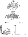
- Figures 1 and 2 show schematically in the sectional view two special embodiments, Figures 3a and 3b the transistor characteristics (100-1000 Hz) without exposure (3b) and with exposure (3a).
- an SiO 2 layer 2 of 30 to 50 nm thickness is produced on a single-crystalline, low-resistance ( ⁇ 0.1 ohm / cm) silicon substrate 1 by thermal oxidation and then at 625 ° C by thermal decomposition of silane (SiH 4 ) an undoped polycrystalline silicon layer 3 of 500 to 1000 nm in thickness. Subsequently, masked diffusion or ion implantation of arsenic ions in a concentration of greater than 1018 cm -3 strongly n + -doped regions 4 and 5, the source (4) and drain zone (5), are produced in the polycrystalline silicon layer 3.
- the arrangement is then provided, in particular in the region of the undoped channel 13 of the polycrystalline layer 3, with a protective oxide 6 made of SiO 2 in a layer thickness of 100 to 200 nm and covered with a passivation layer 7 consisting of silicon nitride or amorphous silicon in a layer thickness of at least 500 nm .
- a protective oxide 6 made of SiO 2 in a layer thickness of 100 to 200 nm and covered with a passivation layer 7 consisting of silicon nitride or amorphous silicon in a layer thickness of at least 500 nm .
- a CVD reaction chemical vapor deposition
- the source (14) and drain connections (15) and the gate connection 8 are attached to the low-resistance substrate 1.
- the substrate 9 is made of amorphous material (e.g. SiO 2 ) and, as described in FIG. 1, is provided with the undoped polycrystalline silicon layer 3 from the vapor phase . Then, as already described in FIG. 1, the source and drain zones 4 and 5 are produced and the surface of the polycrystalline silicon body 3 is converted into a thermally grown oxide layer 2 (SiO 2 layer, layer thickness 30 to 50 nm).
- amorphous material e.g. SiO 2
- the passivation layer 7 consisting of silicon nitride or amorphous silicon is deposited in the glow discharge plasma in a layer thickness of at least 500 nm and the arrangement, as described in FIG Provide corresponding areas of the passivation layer 7 with the source / drain (14, 15) and gate connections (8).
- the threshold voltage drops from ⁇ 20 V to ⁇ 2 V and the mobility increases from ⁇ 0 to ⁇ 10 cm2 / Vs.
Landscapes
- Thin Film Transistor (AREA)
- Light Receiving Elements (AREA)
Applications Claiming Priority (2)
| Application Number | Priority Date | Filing Date | Title |
|---|---|---|---|
| DE19813146981 DE3146981A1 (de) | 1981-11-26 | 1981-11-26 | Fototransistor in mos-duennschichttechnik, verfahren zu seiner herstellung und verfahren zu seinem betrieb. |
| DE3146981 | 1981-11-26 |
Publications (3)
| Publication Number | Publication Date |
|---|---|
| EP0080652A2 true EP0080652A2 (fr) | 1983-06-08 |
| EP0080652A3 EP0080652A3 (en) | 1985-10-23 |
| EP0080652B1 EP0080652B1 (fr) | 1988-08-10 |
Family
ID=6147297
Family Applications (1)
| Application Number | Title | Priority Date | Filing Date |
|---|---|---|---|
| EP82110602A Expired EP0080652B1 (fr) | 1981-11-26 | 1982-11-16 | Phototransistor MOS en technologie à film mince, son procédé de fabrication et sa méthode d'utilisation |
Country Status (4)
| Country | Link |
|---|---|
| US (1) | US4823180A (fr) |
| EP (1) | EP0080652B1 (fr) |
| JP (1) | JPS5897877A (fr) |
| DE (2) | DE3146981A1 (fr) |
Cited By (2)
| Publication number | Priority date | Publication date | Assignee | Title |
|---|---|---|---|---|
| EP0165764A3 (en) * | 1984-06-18 | 1987-03-11 | Xerox Corporation | Depletion mode thin film semiconductor photodetectors |
| GB2192487B (en) * | 1986-07-11 | 1990-09-05 | Canon Kk | Photoelectric conversion device |
Families Citing this family (29)
| Publication number | Priority date | Publication date | Assignee | Title |
|---|---|---|---|---|
| US4727044A (en) | 1984-05-18 | 1988-02-23 | Semiconductor Energy Laboratory Co., Ltd. | Method of making a thin film transistor with laser recrystallized source and drain |
| US4960719A (en) * | 1988-02-04 | 1990-10-02 | Seikosha Co., Ltd. | Method for producing amorphous silicon thin film transistor array substrate |
| GB2215126B (en) * | 1988-02-19 | 1990-11-14 | Gen Electric Co Plc | Process for manufacturing a thin film transistor |
| JPH01217421A (ja) * | 1988-02-26 | 1989-08-31 | Seikosha Co Ltd | 非晶質シリコン薄膜トランジスタアレイ基板およびその製造方法 |
| US5289027A (en) * | 1988-12-09 | 1994-02-22 | Hughes Aircraft Company | Ultrathin submicron MOSFET with intrinsic channel |
| US5012314A (en) * | 1989-03-31 | 1991-04-30 | Mitsubishi Denki Kabushiki Kaisha | Liquid crystal display restoring apparatus |
| US5027177A (en) * | 1989-07-24 | 1991-06-25 | Hughes Aircraft Company | Floating base lateral bipolar phototransistor with field effect gate voltage control |
| US5196911A (en) * | 1990-07-26 | 1993-03-23 | Industrial Technology Research Institute | High photosensitive depletion-gate thin film transistor |
| US5689428A (en) * | 1990-09-28 | 1997-11-18 | Texas Instruments Incorporated | Integrated circuits, transistors, data processing systems, printed wiring boards, digital computers, smart power devices, and processes of manufacture |
| JPH04299578A (ja) * | 1991-03-27 | 1992-10-22 | Canon Inc | 光電変換素子及び薄膜半導体装置 |
| US5567550A (en) * | 1993-03-25 | 1996-10-22 | Texas Instruments Incorporated | Method of making a mask for making integrated circuits |
| US5719065A (en) | 1993-10-01 | 1998-02-17 | Semiconductor Energy Laboratory Co., Ltd. | Method for manufacturing semiconductor device with removable spacers |
| JPH07130974A (ja) * | 1993-11-02 | 1995-05-19 | Semiconductor Energy Lab Co Ltd | 半導体装置およびその動作方法 |
| US5387068A (en) * | 1993-12-06 | 1995-02-07 | Ford Motor Company | Method and system for loading rigid sheet material into shipping containers at a work station and end effector for use therein |
| US5814529A (en) | 1995-01-17 | 1998-09-29 | Semiconductor Energy Laboratory Co., Ltd. | Method for producing a semiconductor integrated circuit including a thin film transistor and a capacitor |
| JP2655126B2 (ja) * | 1995-03-31 | 1997-09-17 | 日本電気株式会社 | 薄膜トランジスタの製造方法 |
| US6420725B1 (en) * | 1995-06-07 | 2002-07-16 | Micron Technology, Inc. | Method and apparatus for forming an integrated circuit electrode having a reduced contact area |
| TW334581B (en) * | 1996-06-04 | 1998-06-21 | Handotai Energy Kenkyusho Kk | Semiconductor integrated circuit and fabrication method thereof |
| EP1020920B1 (fr) | 1999-01-11 | 2010-06-02 | Sel Semiconductor Energy Laboratory Co., Ltd. | Dispositif semiconducteur à transistor à couches minces ayant des transistors de commande et des transistors de pixel sur un substrat commun |
| US6590229B1 (en) * | 1999-01-21 | 2003-07-08 | Semiconductor Energy Laboratory Co., Ltd. | Semiconductor device and process for production thereof |
| US6593592B1 (en) | 1999-01-29 | 2003-07-15 | Semiconductor Energy Laboratory Co., Ltd. | Semiconductor device having thin film transistors |
| US7122835B1 (en) * | 1999-04-07 | 2006-10-17 | Semiconductor Energy Laboratory Co., Ltd. | Electrooptical device and a method of manufacturing the same |
| JP3989761B2 (ja) | 2002-04-09 | 2007-10-10 | 株式会社半導体エネルギー研究所 | 半導体表示装置 |
| US7038239B2 (en) | 2002-04-09 | 2006-05-02 | Semiconductor Energy Laboratory Co., Ltd. | Semiconductor element and display device using the same |
| JP3989763B2 (ja) | 2002-04-15 | 2007-10-10 | 株式会社半導体エネルギー研究所 | 半導体表示装置 |
| TWI270919B (en) | 2002-04-15 | 2007-01-11 | Semiconductor Energy Lab | Display device and method of fabricating the same |
| US7256421B2 (en) | 2002-05-17 | 2007-08-14 | Semiconductor Energy Laboratory, Co., Ltd. | Display device having a structure for preventing the deterioration of a light emitting device |
| WO2011077629A1 (fr) * | 2009-12-25 | 2011-06-30 | シャープ株式会社 | Élément photocapteur, circuit photocapteur, substrat de transistor à couche mince, panneau d'affichage et procédé de fabrication d'élément photocapteur |
| KR101672344B1 (ko) * | 2010-05-20 | 2016-11-04 | 삼성전자주식회사 | 광센싱 회로, 상기 광센싱 회로의 구동 방법, 및 상기 광센싱 회로를 채용한 광센싱 장치 |
Family Cites Families (17)
| Publication number | Priority date | Publication date | Assignee | Title |
|---|---|---|---|---|
| NL6407445A (fr) * | 1964-07-01 | 1966-01-03 | ||
| US3459944A (en) * | 1966-01-04 | 1969-08-05 | Ibm | Photosensitive insulated gate field effect transistor |
| US3514676A (en) * | 1967-10-25 | 1970-05-26 | North American Rockwell | Insulated gate complementary field effect transistors gate structure |
| US3840888A (en) * | 1969-12-30 | 1974-10-08 | Ibm | Complementary mosfet device structure |
| US3704376A (en) * | 1971-05-24 | 1972-11-28 | Inventors & Investors Inc | Photo-electric junction field-effect sensors |
| US3749987A (en) * | 1971-08-09 | 1973-07-31 | Ibm | Semiconductor device embodying field effect transistors and schottky barrier diodes |
| DE2440325A1 (de) * | 1974-08-22 | 1976-03-11 | Siemens Ag | Lichtempfindlicher transistor |
| US4143266A (en) * | 1974-09-13 | 1979-03-06 | Commissariat A L'energie Atomique | Method and device for detecting radiatons |
| JPS5214381A (en) * | 1975-07-25 | 1977-02-03 | Hitachi Ltd | Mis-type semiconductor device |
| JPS52120785A (en) * | 1976-04-05 | 1977-10-11 | Agency Of Ind Science & Technol | Light detection semiconductor device |
| JPS5449082A (en) * | 1977-09-26 | 1979-04-18 | Mitsubishi Electric Corp | Semiconductor device |
| JPS5519850A (en) * | 1978-07-31 | 1980-02-12 | Hitachi Ltd | Semiconductor |
| DE2836911C2 (de) * | 1978-08-23 | 1986-11-06 | Siemens AG, 1000 Berlin und 8000 München | Passivierungsschicht für Halbleiterbauelemente |
| US4272880A (en) * | 1979-04-20 | 1981-06-16 | Intel Corporation | MOS/SOS Process |
| JPS5617083A (en) * | 1979-07-20 | 1981-02-18 | Hitachi Ltd | Semiconductor device and its manufacture |
| JPS5626467A (en) * | 1979-08-10 | 1981-03-14 | Toshiba Corp | Semiconductor device and the manufacturing process |
| JPS5688354A (en) * | 1979-12-20 | 1981-07-17 | Toshiba Corp | Semiconductor integrated circuit device |
-
1981
- 1981-11-26 DE DE19813146981 patent/DE3146981A1/de not_active Withdrawn
-
1982
- 1982-10-28 US US06/437,302 patent/US4823180A/en not_active Expired - Fee Related
- 1982-11-16 DE DE8282110602T patent/DE3278897D1/de not_active Expired
- 1982-11-16 EP EP82110602A patent/EP0080652B1/fr not_active Expired
- 1982-11-25 JP JP57206831A patent/JPS5897877A/ja active Pending
Cited By (3)
| Publication number | Priority date | Publication date | Assignee | Title |
|---|---|---|---|---|
| EP0165764A3 (en) * | 1984-06-18 | 1987-03-11 | Xerox Corporation | Depletion mode thin film semiconductor photodetectors |
| GB2192487B (en) * | 1986-07-11 | 1990-09-05 | Canon Kk | Photoelectric conversion device |
| US5086326A (en) * | 1986-07-11 | 1992-02-04 | Canon Kabushiki Kaisha | Photoelectric conversion device |
Also Published As
| Publication number | Publication date |
|---|---|
| EP0080652B1 (fr) | 1988-08-10 |
| EP0080652A3 (en) | 1985-10-23 |
| DE3146981A1 (de) | 1983-06-01 |
| US4823180A (en) | 1989-04-18 |
| JPS5897877A (ja) | 1983-06-10 |
| DE3278897D1 (en) | 1988-09-15 |
Similar Documents
| Publication | Publication Date | Title |
|---|---|---|
| EP0080652B1 (fr) | Phototransistor MOS en technologie à film mince, son procédé de fabrication et sa méthode d'utilisation | |
| DE69209678T2 (de) | Halbleiteranordnung für Hochspannungsverwendung und Verfahren zur Herstellung | |
| DE69111929T2 (de) | Halbleiteranordnung auf einem dielektrischen isolierten Substrat. | |
| DE2654482C2 (fr) | ||
| DE4226888C2 (de) | Diamant-Feldeffekt-Transistor und Verfahren zu dessen Herstellung | |
| DE19739547A1 (de) | Leistungs-Mosfet mit Heteroübergang und Verfahren für dessen Herstellung | |
| DE102010062721A1 (de) | Halbleiterbauelement mit verbessertem Einschaltwiderstand | |
| DE2845460A1 (de) | Verfahren zur herstellung einer halbleitervorrichtung | |
| DE1614356B2 (de) | Verfahren zur Herstellung einer integrierten Halbleiterbaugruppe mit komplementären Feldeffekttransistoren und Material zur Durchführung des Verfahrens | |
| DE4042163A1 (de) | Verfahren zur herstellung einer halbleitervorrichtung | |
| DE3129539A1 (de) | Bipolartransistor | |
| DE69525558T2 (de) | Methode zur Herstellung eines Dünnfilm-Transistors mit invertierter Struktur | |
| DE112012001612T5 (de) | Bipolartransistor in Siliziumkarbid mit verbesserter Durchbruchsspannung | |
| DE102017201550B4 (de) | Siliciumcarbid-halbleitervorrichtung und verfahren zum herstellen einer siliciumcarbid-halbleitervorrichtung | |
| DE2160462A1 (de) | Halbleiteranordnung und verfahren zur herstellung dieser halbleiteranordnung. | |
| EP0159617B1 (fr) | Procédé pour fabriquer des transistors à effet de champ du type MOS à haute intégration | |
| DE1946302A1 (de) | Integrierte Halbleiterschaltung | |
| DE4445346C2 (de) | Verfahren zur Herstellung eines Heteroübergang-Bipolartransistors | |
| DE2460682A1 (de) | Halbleitervorrichtung | |
| DE1297236B (de) | Verfahren zum Einstellen der Steilheit von Feldeffekttransistoren | |
| DE2541651A1 (de) | Ladungsuebertragungsvorrichtung | |
| DE3119137A1 (de) | Halbleiter und verfahren zu deren herstellung | |
| DE4327132C2 (de) | Dünnfilmtransistor und Verfahren zu dessen Herstellung | |
| EP0075892A2 (fr) | Circuit semi-conducteur intégré ayant une couche semi-conductrice semi-isolante | |
| DE2316118C3 (de) | Verfahren zur Herstellung von Feldeffekttransistoren durch Anwendung einer selektiven Getterung |
Legal Events
| Date | Code | Title | Description |
|---|---|---|---|
| PUAI | Public reference made under article 153(3) epc to a published international application that has entered the european phase |
Free format text: ORIGINAL CODE: 0009012 |
|
| AK | Designated contracting states |
Designated state(s): DE FR GB NL |
|
| 17P | Request for examination filed |
Effective date: 19841119 |
|
| PUAL | Search report despatched |
Free format text: ORIGINAL CODE: 0009013 |
|
| AK | Designated contracting states |
Designated state(s): DE FR GB NL |
|
| 17Q | First examination report despatched |
Effective date: 19870527 |
|
| GRAA | (expected) grant |
Free format text: ORIGINAL CODE: 0009210 |
|
| AK | Designated contracting states |
Kind code of ref document: B1 Designated state(s): DE FR GB NL |
|
| GBT | Gb: translation of ep patent filed (gb section 77(6)(a)/1977) | ||
| REF | Corresponds to: |
Ref document number: 3278897 Country of ref document: DE Date of ref document: 19880915 |
|
| ET | Fr: translation filed | ||
| PLBE | No opposition filed within time limit |
Free format text: ORIGINAL CODE: 0009261 |
|
| STAA | Information on the status of an ep patent application or granted ep patent |
Free format text: STATUS: NO OPPOSITION FILED WITHIN TIME LIMIT |
|
| 26N | No opposition filed | ||
| PGFP | Annual fee paid to national office [announced via postgrant information from national office to epo] |
Ref country code: FR Payment date: 19891124 Year of fee payment: 8 |
|
| PGFP | Annual fee paid to national office [announced via postgrant information from national office to epo] |
Ref country code: NL Payment date: 19891130 Year of fee payment: 8 |
|
| PGFP | Annual fee paid to national office [announced via postgrant information from national office to epo] |
Ref country code: DE Payment date: 19900126 Year of fee payment: 8 |
|
| PGFP | Annual fee paid to national office [announced via postgrant information from national office to epo] |
Ref country code: GB Payment date: 19901018 Year of fee payment: 9 |
|
| PG25 | Lapsed in a contracting state [announced via postgrant information from national office to epo] |
Ref country code: NL Effective date: 19910601 |
|
| NLV4 | Nl: lapsed or anulled due to non-payment of the annual fee | ||
| PG25 | Lapsed in a contracting state [announced via postgrant information from national office to epo] |
Ref country code: FR Effective date: 19910731 |
|
| PG25 | Lapsed in a contracting state [announced via postgrant information from national office to epo] |
Ref country code: DE Effective date: 19910801 |
|
| REG | Reference to a national code |
Ref country code: FR Ref legal event code: ST |
|
| PG25 | Lapsed in a contracting state [announced via postgrant information from national office to epo] |
Ref country code: GB Effective date: 19911116 |
|
| GBPC | Gb: european patent ceased through non-payment of renewal fee |