EP0083387B1 - Speicheranordnung - Google Patents
Speicheranordnung Download PDFInfo
- Publication number
- EP0083387B1 EP0083387B1 EP82105768A EP82105768A EP0083387B1 EP 0083387 B1 EP0083387 B1 EP 0083387B1 EP 82105768 A EP82105768 A EP 82105768A EP 82105768 A EP82105768 A EP 82105768A EP 0083387 B1 EP0083387 B1 EP 0083387B1
- Authority
- EP
- European Patent Office
- Prior art keywords
- floating gate
- fet
- gate
- control gate
- volatile
- Prior art date
- Legal status (The legal status is an assumption and is not a legal conclusion. Google has not performed a legal analysis and makes no representation as to the accuracy of the status listed.)
- Expired
Links
- 230000015654 memory Effects 0.000 claims description 18
- 230000009977 dual effect Effects 0.000 claims description 7
- 239000000758 substrate Substances 0.000 claims description 6
- 239000003990 capacitor Substances 0.000 claims description 5
- 239000004065 semiconductor Substances 0.000 claims description 5
- 238000007599 discharging Methods 0.000 claims 1
- VYPSYNLAJGMNEJ-UHFFFAOYSA-N silicon dioxide Inorganic materials O=[Si]=O VYPSYNLAJGMNEJ-UHFFFAOYSA-N 0.000 description 13
- 238000009792 diffusion process Methods 0.000 description 11
- 229910052681 coesite Inorganic materials 0.000 description 10
- 229910052906 cristobalite Inorganic materials 0.000 description 10
- 229910052682 stishovite Inorganic materials 0.000 description 10
- 229910052905 tridymite Inorganic materials 0.000 description 10
- 239000012212 insulator Substances 0.000 description 9
- 229910021420 polycrystalline silicon Inorganic materials 0.000 description 4
- 229910052581 Si3N4 Inorganic materials 0.000 description 3
- 230000005684 electric field Effects 0.000 description 3
- 230000005669 field effect Effects 0.000 description 3
- 238000004519 manufacturing process Methods 0.000 description 3
- 229920005591 polysilicon Polymers 0.000 description 3
- HQVNEWCFYHHQES-UHFFFAOYSA-N silicon nitride Chemical compound N12[Si]34N5[Si]62N3[Si]51N64 HQVNEWCFYHHQES-UHFFFAOYSA-N 0.000 description 3
- 230000003068 static effect Effects 0.000 description 3
- XUIMIQQOPSSXEZ-UHFFFAOYSA-N Silicon Chemical compound [Si] XUIMIQQOPSSXEZ-UHFFFAOYSA-N 0.000 description 2
- 229910052710 silicon Inorganic materials 0.000 description 2
- 239000010703 silicon Substances 0.000 description 2
- 239000000377 silicon dioxide Substances 0.000 description 2
- QVGXLLKOCUKJST-UHFFFAOYSA-N atomic oxygen Chemical compound [O] QVGXLLKOCUKJST-UHFFFAOYSA-N 0.000 description 1
- 230000015572 biosynthetic process Effects 0.000 description 1
- 239000011195 cermet Substances 0.000 description 1
- 230000000694 effects Effects 0.000 description 1
- 238000005530 etching Methods 0.000 description 1
- 230000006870 function Effects 0.000 description 1
- 239000012535 impurity Substances 0.000 description 1
- 238000002347 injection Methods 0.000 description 1
- 239000007924 injection Substances 0.000 description 1
- 239000000463 material Substances 0.000 description 1
- 238000001465 metallisation Methods 0.000 description 1
- 238000000034 method Methods 0.000 description 1
- 230000003647 oxidation Effects 0.000 description 1
- 238000007254 oxidation reaction Methods 0.000 description 1
- 229910052760 oxygen Inorganic materials 0.000 description 1
- 239000001301 oxygen Substances 0.000 description 1
- 230000000717 retained effect Effects 0.000 description 1
- 235000012239 silicon dioxide Nutrition 0.000 description 1
Images


Classifications
-
- G—PHYSICS
- G11—INFORMATION STORAGE
- G11C—STATIC STORES
- G11C14/00—Digital stores characterised by arrangements of cells having volatile and non-volatile storage properties for back-up when the power is down
-
- H—ELECTRICITY
- H10—SEMICONDUCTOR DEVICES; ELECTRIC SOLID-STATE DEVICES NOT OTHERWISE PROVIDED FOR
- H10D—INORGANIC ELECTRIC SEMICONDUCTOR DEVICES
- H10D30/00—Field-effect transistors [FET]
- H10D30/60—Insulated-gate field-effect transistors [IGFET]
- H10D30/68—Floating-gate IGFETs
- H10D30/681—Floating-gate IGFETs having only two programming levels
- H10D30/682—Floating-gate IGFETs having only two programming levels programmed by injection of carriers through a conductive insulator, e.g. Poole-Frankel conduction
Definitions
- This invention relates to non-volatile semiconductor memory devices and more particularly to devices which utilize a device having a floating gate.
- NVRAM non-volatile random access memories
- a number of circuits have evolved which take advantage ofthe abilityoffield effect transistors to store charge and thus serve as memory cells.
- Such cells may be either dynamic or static in nature.
- the dynamic cells may employ only a single field effect transistor and the static cells may be arranged in a flip-flop configuration, as is well known.
- Each of these types of cells may be referred to as volatile cells since information stored in these cells is lost when the power supply voltage applied to the memory is lost or turned off.
- an alternate power supply such as a battery system, must be coupled to the memory for use in the event of failure of the main power supply.
- CMOS complementary metal-nitride-oxide-silicon structure
- CMOS complementary metal-nitride-oxide-silicon structure
- CMOS complementary metal-nitride-oxide-silicon structure
- non-volatile memory cells which use non-volatile MNOS transistors or devices are capable of retaining information for moderate periods of time stored volatilely in a cell but these devices require high voltage pulses for writing and erasing the information, they are slow and they require rather complex processes for their fabrication.
- An example of a non-volatile semiconductor memory cell is taught in U.S. Patent 3,676,717, filed November 2, 1970.
- Non-volatile memory cells which use conventionally arranged floating gate devices are also capable of preserving for long periods of time information stored volatilely in a cell but these devices likewise have required high voltage pulses for writing and erasing the information, they have been slow and required high currents, approximately one milliampere per device, to write.
- An example of a known non-volatile semiconductor memory cell having incorporated therein a floating gate is taught in U.S. Patent 4,207,615, filed November 17, 1978.
- non-volatile static memories which include a volatile circuit coupled to a non-volatile device, (akin to that of the present invention), having a floating gate and first and second control gates capacitively coupled to the floating gate with a charge injector structure including enhanced conduction insulators disposed between the floating gate and one of the two control gates.
- RAM random access memory
- EP-A-55799 there is provided one such improved one device dynamic volatile memory cell having the capability of storing data non-volatilely.
- the device uses a floating gate for storing information non-volatilely during power failure. To recover data after power has been restored, charge is transferred from a floating gate back to a storage node whereby the charge is partially depleted. In the most optimal case at ideal conditions the resultant charge is only 25% of the original stored charge. Therefore, in order to insure that the resultant signal is sufficiently large for sensing, the storage capacitance has to be at least 4 times larger than normal to insure a signal strong enough to be detected. Consequently large cell sizes are required.
- a floating gate memory device combines a dynamic random access memory (RAM), see reference to R. H. Dennard, with a dual electron-injector structure (DEIS) see the hereinabove cited IEEE Electron Device Letters article.
- the DEIS is associated with the FET floating gate portion of the dynamic RAM device.
- the floating gate FET is normally at a conductive state.
- the floating gate FET is charged with electrons via the DEIS according to whether data is stored in the volatile memory or not.
- the data is retrieved by sensing whether the floating gate FET is in a conductive state or in a nonconductive state, which depends on the stored non-volatile charge on the floating gate.
- the non-volatile storage can be erased independently.
- a non-volatile dynamic RAM device of the present invention generally designated 10.
- the non volatile memory portion of the device comprises control gate 12, floating gate 14 and a p type silicon substrate 16.
- DEIS stack 18 Situated between floating gate 14 and substrate 16 is DEIS stack 18.
- This DEIS stack 18 is comprised of an insulator having a first SI rich region 20 and second Si rich region 24, separated by said insulator 22.
- the structures will be thought of as being a Si rich Si0 2 region, a SiO 2 region, separating a second Si rich Si0 2 region.
- One skilled in the art would certainly know that other similar cermet type materials could also be used in place of the Si-rich Si0 2 .
- the DEIS 18 is fabricated so as to be placed on a first N + diffusion region 26 in substrate 16.
- the N + diffusion region 26 is connected to a second N + source diffusion region 28.
- Contact 37 is connected to the N + region 28.
- region 28 is a terminal region of the channel of FET 38.
- the random access memory or RAM portion of the device is comprised of storage capacitor 30 which consists of plate 32 and a third N * diffusion 34 also known as a storage node separated by insulator 36, and a FET switch 38 is formed between source diffusion 28 and storage node 34, with a control gate 12. Contact 35 is connected with plate 32 of storage capacitor 30.
- the device of FIG. 1 functions as a dynamic RAM device.
- electrons are written onto floating gate 14, normally a doped polysilicon region, by raising the voltage on control gate 12 to a higher positive voltage than used for the normal mode of dynamic RAM operation.
- This operation turns on the second or lower Si rich region 24 of the DEIS 18, which via localized enhanced electric fields at the lower Si-rich Si0 2 region-insulator interface, injects electrons into the insulator layer 22.
- These electrons due to the applied electrical field flow to floating gate 14, where they are stored.
- These stored electrons can be erased by lowering the control gate potential to ground and by raising the potential of source region 26 to a positive voltage.
- the first Si-rich Si0 2 injector 20 ejects electrons from gate 14 via localized enhanced electric fields at its interface into the intervening Si0 2 layer and which flow therefrom to the N * diffusion region 26.
- Write and erase operations can be performed with voltages in the range from 5V to 30V in times from 5 msec to 5 nsec depending on the DEIS stack configuration and device geometry as discussed in the paper entitled, "Electrically-Alterable Read-Only-Memory Using Si-Rich Si0 2 Injectors and a Floating Polycrystalline Silicon Storage Layer", by D. J. DiMaria et al, which appeared in the Journal of Applied Physics, Vol. 52, pp. 4825-4842, July 1981.
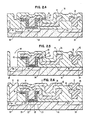
- FIGS. 2.1 to 2.6 there is shown as an example a schematic of a method of fabricating the device in FIG. 1.
- FIG. 2.1 there is provided P type substrate 16 having disposed therein N * diffusion regions 26 and 28.
- First an oxide layer 36 is grown atop substrate 16, and then it is delineated, and etched prior to diffusion and drive in of the N + diffusions 26 and 28.
- the N + diffusion 34 is formed prior to oxide growth.
- the DEIS stack 18 is deposited and covered with a silicon nitride oxidation mask 40.
- the mask 40 is delineated and etched and oxide is etched as shown in FIG. 2.3.
- the silicon nitride mask 40 is then removed by etching.
- a polysilicon film is then deposited, doped with an N * type impurity, and delineated (FIG. 2.4).
- This polysilicon film thereby forms floating gate 14 and plate 32.
- a thick oxide layer 36 is then deposited.
- the exposed portion of the DEIS stack 18 is converted to oxide during this step by the oxygen ambient.
- contact holes 42 and 44 are delineated and etched as shown in FIG. 2.5.
- metallization is effected for the formation of the control gate 12 and for contacts 37 and 35 to N + source diffusion 28 and dynamic RAM storage capacitor plate 32 as shown in FIG. 2.6.
- FIG. 3 there is shown an alternate embodiment of the present invention.
- the device shown therein is similar to that of FIG. 1, except that DEIS stack is now situated between floating gate 14 and control gate 12.
- the write or erase operations for the non-volatile memory portion of the device are performed by applying a negative or positive voltage pulse to the control gate electrode, respectively. This will either put electrons on or take electrons off the floating gate portion of the device.
- the voltage range again can be from ⁇ 5V to ⁇ 30V with the switching times in the range from 5msec to 5nsec depending on the DEIS stack configuration and electrode geometry.
Landscapes
- Semiconductor Memories (AREA)
- Static Random-Access Memory (AREA)
- Read Only Memory (AREA)
- Non-Volatile Memory (AREA)
Claims (7)
Applications Claiming Priority (2)
| Application Number | Priority Date | Filing Date | Title |
|---|---|---|---|
| US06/336,463 US4471471A (en) | 1981-12-31 | 1981-12-31 | Non-volatile RAM device |
| US336463 | 1981-12-31 |
Publications (3)
| Publication Number | Publication Date |
|---|---|
| EP0083387A2 EP0083387A2 (de) | 1983-07-13 |
| EP0083387A3 EP0083387A3 (en) | 1986-04-09 |
| EP0083387B1 true EP0083387B1 (de) | 1988-06-01 |
Family
ID=23316199
Family Applications (1)
| Application Number | Title | Priority Date | Filing Date |
|---|---|---|---|
| EP82105768A Expired EP0083387B1 (de) | 1981-12-31 | 1982-06-29 | Speicheranordnung |
Country Status (4)
| Country | Link |
|---|---|
| US (1) | US4471471A (de) |
| EP (1) | EP0083387B1 (de) |
| JP (1) | JPS602783B2 (de) |
| DE (1) | DE3278591D1 (de) |
Families Citing this family (23)
| Publication number | Priority date | Publication date | Assignee | Title |
|---|---|---|---|---|
| JPS59112657A (ja) * | 1982-09-30 | 1984-06-29 | フエアチアイルド・カメラ・アンド・インストルメント・コ−ポレ−シヨン | 書込可能なリ−ドオンリ−メモリ |
| US4688078A (en) * | 1982-09-30 | 1987-08-18 | Ning Hseih | Partially relaxable composite dielectric structure |
| US4654825A (en) * | 1984-01-06 | 1987-03-31 | Advanced Micro Devices, Inc. | E2 prom memory cell |
| US4717943A (en) * | 1984-06-25 | 1988-01-05 | International Business Machines | Charge storage structure for nonvolatile memories |
| US4656729A (en) * | 1985-03-25 | 1987-04-14 | International Business Machines Corp. | Dual electron injection structure and process with self-limiting oxidation barrier |
| JPS61245578A (ja) * | 1985-04-23 | 1986-10-31 | Seiko Instr & Electronics Ltd | 半導体不揮発性メモリ |
| JP2605082B2 (ja) * | 1988-02-26 | 1997-04-30 | 株式会社日立製作所 | 半導体集積回路装置の製造方法 |
| CA1276314C (en) * | 1988-03-24 | 1990-11-13 | Alexander Kalnitsky | Silicon ion implanted semiconductor device |
| DE3816358A1 (de) * | 1988-05-13 | 1989-11-23 | Eurosil Electronic Gmbh | Nichtfluechtige speicherzelle und verfahren zur herstellung |
| US5146431A (en) * | 1990-09-20 | 1992-09-08 | Sharp Kabushiki Kaisha | Method and apparatus for page recall of data in an nonvolatile DRAM memory device |
| US5331188A (en) * | 1992-02-25 | 1994-07-19 | International Business Machines Corporation | Non-volatile DRAM cell |
| US5399516A (en) * | 1992-03-12 | 1995-03-21 | International Business Machines Corporation | Method of making shadow RAM cell having a shallow trench EEPROM |
| US5467305A (en) * | 1992-03-12 | 1995-11-14 | International Business Machines Corporation | Three-dimensional direct-write EEPROM arrays and fabrication methods |
| US5196722A (en) * | 1992-03-12 | 1993-03-23 | International Business Machines Corporation | Shadow ram cell having a shallow trench eeprom |
| US5606177A (en) * | 1993-10-29 | 1997-02-25 | Texas Instruments Incorporated | Silicon oxide resonant tunneling diode structure |
| US5432749A (en) * | 1994-04-26 | 1995-07-11 | National Semiconductor Corporation | Non-volatile memory cell having hole confinement layer for reducing band-to-band tunneling |
| TW587251B (en) * | 1999-10-04 | 2004-05-11 | Koninkl Philips Electronics Nv | A non-volatile MOS RAM cell with capacitor-isolated nodes that are radiation accessible for rendering a non-permanent programmed information in the cell a non-volatile one |
| US6445029B1 (en) | 2000-10-24 | 2002-09-03 | International Business Machines Corporation | NVRAM array device with enhanced write and erase |
| KR100719178B1 (ko) * | 2003-08-29 | 2007-05-17 | 주식회사 하이닉스반도체 | 비휘발성 디램의 구동방법 |
| TWI254313B (en) * | 2003-12-30 | 2006-05-01 | Hynix Semiconductor Inc | Driving circuit for non-volatile dram |
| US7816722B2 (en) * | 2004-02-04 | 2010-10-19 | Hewlett-Packard Development Company, L.P. | Memory array |
| US7678662B2 (en) * | 2005-12-13 | 2010-03-16 | Applied Materials, Inc. | Memory cell having stressed layers |
| US9214465B2 (en) | 2012-07-24 | 2015-12-15 | Flashsilicon Incorporation | Structures and operational methods of non-volatile dynamic random access memory devices |
Family Cites Families (12)
| Publication number | Priority date | Publication date | Assignee | Title |
|---|---|---|---|---|
| US3387286A (en) * | 1967-07-14 | 1968-06-04 | Ibm | Field-effect transistor memory |
| US3676717A (en) * | 1970-11-02 | 1972-07-11 | Ncr Co | Nonvolatile flip-flop memory cell |
| US3811076A (en) * | 1973-01-02 | 1974-05-14 | Ibm | Field effect transistor integrated circuit and memory |
| DE2450116C2 (de) * | 1974-10-22 | 1976-09-16 | Siemens AG, 1000 Berlin und 8000 München | Dynamisches Ein-Transistor-Speicherelement für nichtflüchtige Speicher und Verfahren zu seinem Betrieb |
| US3916390A (en) * | 1974-12-31 | 1975-10-28 | Ibm | Dynamic memory with non-volatile back-up mode |
| US4175291A (en) * | 1976-08-16 | 1979-11-20 | Ncr Corporation | Non-volatile random access memory cell |
| US4207615A (en) * | 1978-11-17 | 1980-06-10 | Intel Corporation | Non-volatile ram cell |
| US4217601A (en) * | 1979-02-15 | 1980-08-12 | International Business Machines Corporation | Non-volatile memory devices fabricated from graded or stepped energy band gap insulator MIM or MIS structure |
| US4257056A (en) * | 1979-06-27 | 1981-03-17 | National Semiconductor Corporation | Electrically erasable read only memory |
| US4399522A (en) * | 1980-09-30 | 1983-08-16 | International Business Machines Corporation | Non-volatile static RAM cell with enhanced conduction insulators |
| US4388704A (en) * | 1980-09-30 | 1983-06-14 | International Business Machines Corporation | Non-volatile RAM cell with enhanced conduction insulators |
| US4363110A (en) * | 1980-12-22 | 1982-12-07 | International Business Machines Corp. | Non-volatile dynamic RAM cell |
-
1981
- 1981-12-31 US US06/336,463 patent/US4471471A/en not_active Expired - Lifetime
-
1982
- 1982-06-29 DE DE8282105768T patent/DE3278591D1/de not_active Expired
- 1982-06-29 EP EP82105768A patent/EP0083387B1/de not_active Expired
- 1982-08-05 JP JP57135809A patent/JPS602783B2/ja not_active Expired
Also Published As
| Publication number | Publication date |
|---|---|
| US4471471A (en) | 1984-09-11 |
| EP0083387A3 (en) | 1986-04-09 |
| JPS58119667A (ja) | 1983-07-16 |
| JPS602783B2 (ja) | 1985-01-23 |
| EP0083387A2 (de) | 1983-07-13 |
| DE3278591D1 (en) | 1988-07-07 |
Similar Documents
| Publication | Publication Date | Title |
|---|---|---|
| EP0083387A2 (de) | Speicheranordnung | |
| US5446299A (en) | Semiconductor random access memory cell on silicon-on-insulator with dual control gates | |
| US4274012A (en) | Substrate coupled floating gate memory cell | |
| US5892709A (en) | Single level gate nonvolatile memory device and method for accessing the same | |
| US7440310B2 (en) | Memory cell with trenched gated thyristor | |
| JP3710082B2 (ja) | メモリ・トランジスタを作成する方法 | |
| EP0253631B1 (de) | Halbleiterspeicheranordnung | |
| JP3473953B2 (ja) | 不揮発性ランダムアクセス・メモリ装置 | |
| US5506431A (en) | Double poly trenched channel accelerated tunneling electron (DPT-CATE) cell, for memory applications | |
| US5065201A (en) | Semiconductor memory device | |
| EP0557581A2 (de) | Nichtflüchtige DRAM-Zelle | |
| EP0083386B1 (de) | Speicherzelle | |
| JPH0343792B2 (de) | ||
| JPS637031B2 (de) | ||
| EP0198040B1 (de) | Nichtflüchtige speicherzelle | |
| EP0055799B1 (de) | Nichtflüchtige dynamische RAM-Speicherzelle | |
| US4257056A (en) | Electrically erasable read only memory | |
| EP0177816B1 (de) | Nichtflüchtige dynamische Schreib-/Lesespeicher mit wahlfreiem Zugriff | |
| US4665417A (en) | Non-volatile dynamic random access memory cell | |
| EP0105802A2 (de) | Programmierbarer Nurlesespeicher | |
| EP0481392B1 (de) | Nichtflüchtige Halbleiterspeicheranordnung | |
| US4622570A (en) | Semiconductor memory | |
| EP0387102A2 (de) | Nichtflüchtiger Halbleiterspeicher und Schreibverfahren dafür | |
| EP0048815A2 (de) | Statische, nichtflüchtige Halbleiterspeicherzelle | |
| EP0021777B1 (de) | Nicht-flüchtige Halbleiter-Speichervorrichtung |
Legal Events
| Date | Code | Title | Description |
|---|---|---|---|
| PUAI | Public reference made under article 153(3) epc to a published international application that has entered the european phase |
Free format text: ORIGINAL CODE: 0009012 |
|
| AK | Designated contracting states |
Designated state(s): DE FR GB NL SE |
|
| 17P | Request for examination filed |
Effective date: 19831021 |
|
| PUAL | Search report despatched |
Free format text: ORIGINAL CODE: 0009013 |
|
| AK | Designated contracting states |
Kind code of ref document: A3 Designated state(s): DE FR GB NL SE |
|
| 17Q | First examination report despatched |
Effective date: 19870319 |
|
| GRAA | (expected) grant |
Free format text: ORIGINAL CODE: 0009210 |
|
| AK | Designated contracting states |
Kind code of ref document: B1 Designated state(s): DE FR GB NL SE |
|
| REF | Corresponds to: |
Ref document number: 3278591 Country of ref document: DE Date of ref document: 19880707 |
|
| ET | Fr: translation filed | ||
| PLBE | No opposition filed within time limit |
Free format text: ORIGINAL CODE: 0009261 |
|
| STAA | Information on the status of an ep patent application or granted ep patent |
Free format text: STATUS: NO OPPOSITION FILED WITHIN TIME LIMIT |
|
| 26N | No opposition filed | ||
| PGFP | Annual fee paid to national office [announced via postgrant information from national office to epo] |
Ref country code: GB Payment date: 19920506 Year of fee payment: 11 |
|
| PGFP | Annual fee paid to national office [announced via postgrant information from national office to epo] |
Ref country code: SE Payment date: 19920525 Year of fee payment: 11 |
|
| PGFP | Annual fee paid to national office [announced via postgrant information from national office to epo] |
Ref country code: FR Payment date: 19920601 Year of fee payment: 11 |
|
| PGFP | Annual fee paid to national office [announced via postgrant information from national office to epo] |
Ref country code: DE Payment date: 19920619 Year of fee payment: 11 |
|
| PGFP | Annual fee paid to national office [announced via postgrant information from national office to epo] |
Ref country code: NL Payment date: 19920630 Year of fee payment: 11 |
|
| PG25 | Lapsed in a contracting state [announced via postgrant information from national office to epo] |
Ref country code: GB Effective date: 19930629 |
|
| PG25 | Lapsed in a contracting state [announced via postgrant information from national office to epo] |
Ref country code: SE Effective date: 19930630 |
|
| PG25 | Lapsed in a contracting state [announced via postgrant information from national office to epo] |
Ref country code: NL Effective date: 19940101 |
|
| NLV4 | Nl: lapsed or anulled due to non-payment of the annual fee | ||
| GBPC | Gb: european patent ceased through non-payment of renewal fee |
Effective date: 19930629 |
|
| PG25 | Lapsed in a contracting state [announced via postgrant information from national office to epo] |
Ref country code: FR Effective date: 19940228 |
|
| PG25 | Lapsed in a contracting state [announced via postgrant information from national office to epo] |
Ref country code: DE Effective date: 19940301 |
|
| REG | Reference to a national code |
Ref country code: FR Ref legal event code: ST |
|
| EUG | Se: european patent has lapsed |
Ref document number: 82105768.4 Effective date: 19940110 |