EP0085974A2 - Procédé de formation d'une pluralité de zones de brasure sur une plaquette semi-conductrice - Google Patents
Procédé de formation d'une pluralité de zones de brasure sur une plaquette semi-conductrice Download PDFInfo
- Publication number
- EP0085974A2 EP0085974A2 EP83101135A EP83101135A EP0085974A2 EP 0085974 A2 EP0085974 A2 EP 0085974A2 EP 83101135 A EP83101135 A EP 83101135A EP 83101135 A EP83101135 A EP 83101135A EP 0085974 A2 EP0085974 A2 EP 0085974A2
- Authority
- EP
- European Patent Office
- Prior art keywords
- solder
- semiconductor wafer
- regions
- foil
- forming
- Prior art date
- Legal status (The legal status is an assumption and is not a legal conclusion. Google has not performed a legal analysis and makes no representation as to the accuracy of the status listed.)
- Granted
Links
Images


Classifications
-
- H—ELECTRICITY
- H10—SEMICONDUCTOR DEVICES; ELECTRIC SOLID-STATE DEVICES NOT OTHERWISE PROVIDED FOR
- H10W—GENERIC PACKAGES, INTERCONNECTIONS, CONNECTORS OR OTHER CONSTRUCTIONAL DETAILS OF DEVICES COVERED BY CLASS H10
- H10W72/00—Interconnections or connectors in packages
- H10W72/01—Manufacture or treatment
- H10W72/012—Manufacture or treatment of bump connectors, dummy bumps or thermal bumps
-
- H—ELECTRICITY
- H10—SEMICONDUCTOR DEVICES; ELECTRIC SOLID-STATE DEVICES NOT OTHERWISE PROVIDED FOR
- H10W—GENERIC PACKAGES, INTERCONNECTIONS, CONNECTORS OR OTHER CONSTRUCTIONAL DETAILS OF DEVICES COVERED BY CLASS H10
- H10W72/00—Interconnections or connectors in packages
- H10W72/20—Bump connectors, e.g. solder bumps or copper pillars; Dummy bumps; Thermal bumps
- H10W72/251—Materials
Definitions
- the present invention relates to an improvement of a method of forming a number of solder layers on one or both major surfaces of a semiconductor wafer.
- a drawback to be first mentioned is seen in the fact that the amount of deposited solder is uneven among the solder layers.
- the amount of solder deposited wettingly on the ohmic contacts will vary in dependence on an angle and a speed at which the semiconductor wafer is lifted or withdrawn upwardly from the molten solder bath as well as the temperature thereof.
- it is difficult to control the amount or quantity of solder deposited through wetting so that uniform thickness be attained for all the solder layers.
- a reduced quantity of the deposited solder will naturally result in a thin solder layer.
- a semiconductor device is to be constituted by a plurality of semiconductor elements disposed between rows of leads arrayed in opposition to each other with an equal distance between the leads in each row, which leads are attached to the respective semiconductor elements
- uneveness in the thickness of the solder layers will involve uneveness among the individual semiconductor elements in respect of the contact area over which the lead is contacted to the solder layer, whereby the thermal and the electrical characteristics are made unbalanced among the semiconductor elements.
- a second drawback resides in that the surface of the molten solder mass constituting the solder layer tends to be spherical under the surface tension.
- the lead to be attached may be inclined or positionally mis-aligned relative to the ohmic contact, providing an obstacle to attaining the desired structure of lead attachment. This problem is particularly serious when a plurality of semiconductor devices disposed between rows of the leads are to be attached with the leads.
- An object of the present invention is to provide a method of forming a number of discrete solder layers on a semiconductor wafer, in which the drawbacks of the prior art methods described above are eliminated.
- Another object of the present invention is to provide a method of forming a plurality of discrete solder layers on a semiconductor wafer, which solder layers are uniform in thickness and present flat top surfaces, respectively.
- a still further object of the present invention is to provide a method which is capable of forming a number of discrete solder layers on a semiconductor wafer having a uniformed thickness and presenting flat top surfaces with an improved reproducibility.
- a first feature of the method of forming discrete solder layers on a semiconductor wafer according to the invention resides in that those portions of one major surface of the semiconductor wafer having a large area on which the discrete solder layers are to be formed are rendered easier to be wetted with solder than the remaining portions, and a solder foil is disposed on the one major surface of the wafer to be subsequently heated. More specifically, those portions of the one major surface of the semiconductor wafer on which the solder layers are to be formed are provided with metal electrodes which can be ohmic-contacted to the semiconductor wafer and are easy to be wetted with solder, while at the remaining portions the surface of the semiconductor wafer is exposed as it is or alternatively coated with an insulation film.
- the solder foil After the solder foil has been disposed on the semiconductor wafer, the stacked structure or assembly is heated. As the consequence, molten solder is gathered on each of the metal electrodes under surface tension, whereby a number of separated or discrete solder layers are formed on the semiconductor wafer.
- the solder foil should preferably be realized in a net-like structure and disposed on the semiconductor wafer in such a manner that the center of each of meshes formed in the solder foil is located essentially at the center of an area defined by the adjacent metal electrodes among them, in order to assure the melting separation of the solder foil (i.e. separation of the solder foil into the discrete solder layers through melting of the former) in a satisfactory manner.
- the solder foil thus prepared is disposed on the semiconductor wafer to be subsequently subjected to the heating process.
- the solder foil prepared so as to meet the above geometrical or positional requirement is composed of solder foil portions provided in correspondence to the metal electrodes, respectively, and interconnecting portions or bridge portions for connecting or linking the solder foil portions to one another.
- the solder foil portion should preferably be of a slightly smaller area than that of the metal electrode so that solder material constituting the interconnection or bridge is also permitted to gather on the metal electrode when it is molten, to thereby assure the beakage of the interconnecting portion without fail. Further, it is preferred that the interconnecting bridge portion has a narrowed or constricted mid portion so that the breakage thereof through melting takes place at the well defined location, because the thickness of the solder layer as formed can then be made uniform more positively for all the metal electrodes.
- the step of separating or fragmenting the solder foil disposed on the semiconductor wafer into the discrete solder layers through melting is carried out in such a situation that the discrete solder layers may have a uniformed thickness and present respective flat top surfaces.
- a plate-like jig composed of a plate having a plurality of projections or protrusions which have a height equal to the thickness of the solder layer to be formed is disposed on the solder foil placed on the semiconductor wafer.
- the stacked assembly is subsequently heated to a melting temperature.
- the plate-like jig may be made of a material which is difficult to be wetted with solder and capable of withstanding the melting temperature of the solder material.
- the discrete solder layers will be formed simultaneously on a number of semiconductor wafers at both major surfaces thereof through the melting separation process.
- a single plate-like jig provided with the projections on both surfaces may be used for both the overlying and the underlying semiconductor wafers.
- the step of separating the solder foil disposed on the semiconductor wafer into the discrete solder layers through melting is carried out in non-oxidizing atmosphere. More specifically, the melting separation step is conducted in the atmosphere of an innert gas, a reducing gas or a gas mixture thereof.
- the melting separation step is carried out in the atmosphere of a reducing gas, the wettability to solder as well as the surface tension can be enhanced to allow the melting separation process to be effected smoothly.
- the finished solder layers present pure and clear surfaces, facilitating attachment of leads, to a further advantage.
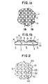
- Figs. 1 to 5 are views which illustrate steps involved in carrying out the method according to a preferred embodiment of the invention.
- a semiconductor wafer 1 of a large area in which a desired pn-juction is formed undergoes a treatment through which those portions of both major surfaces 11 and 12 of the semiconductor wafer 1 where solder layers are to be formed are rendered easy to be wetted with solder while the other portions being made difficult to be wetted with solder.
- a plurality of grooves 13 are formed in the one major surface 11 in such an array that the grooves 13 extend orthogonally in X- and Y-directions with the adjacent grooves being spaced at a substantially equal distance, whereby there are.produced a large number of mesa-like portions 14 each of a square surface in a matrix-like array, being partitioned from one another by the surrounding grooves.
- a metal electrode formed of a material exhibiting high wettability to the solder such as, for example, Ni, an alloy of Cr - Ni - Ag or the like.
- Similar metal electrodes 3 are also formed on the other major surface 12 of the semiconductor wafer 1 at locations corresponding to the mesa-like portions 14 in opposition thereto, respectively.
- the surfaces of the grooves 13 are covered with a passivation film 4 such as a glass film.
- the remaining portions of both the major surfaces are covered with a Si0 2 - film 5. Since the glass film 4 as well as the Si0 2 - film 5 is intrinsically poor in wettability to the solder, they are certainly effected in reducing the wettability to the solder at the portions covered with these films. It should however be noted that the inherent function of these films resides in passivating the active surfaces of the semiconductor surface. In other words, even when these portions of the semiconductor wafer are exposed as they are because of no passivation being required, the exposed surfaces can nevertheless be made difficult to be wetted with solder by virtue of the structure mentioned above.
- Fig. 2 illustrates a step for preparing a net-like solder foil 6 which has a uniform thickness and is provided with a number of circular or round meshes 61 formed and arrayed at the same pitch as the mesa-like portions 14 of the semiconductor wafer 1.
- the solder foil 6 may be considered to be constituted by a number of solder foil portions 62 arrayed in correspondence to the mesa-like portions 14 of the semiconductor wafer 1 and interconnecting portions or bridges 63 which connect the adjacent solder foil portions to one another.
- Each of the solder foil portions 62 is realized in an area smaller than that of the metal electrodes 2 and 3, while the interconnecting portion 63 is so formed as to present an intermediate portion of a reduced width as compared with the other portions thereof.
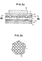
- Figs. 3a and 3b illustrate steps at which the solder foils 6 are positioned over both the major surfaces of the semiconductor wafer 1.
- a reference numeral 7 denotes a jig plate provided with a predetermined number of protrusions 71 each of a predetermined height.
- the solder foils 6 are positioned on both the major surfaces of the semiconductor wafer 1; respectively, in such a disposition that the solder foil portions 62 coincide with the metal electrodes 2 and 3, respectively, while the meshes 61 coincide, respectively, with those areas each defined among a quartet of the metal electrodes located adjacent to one another. More specifically, the solder foil 6 is positioned on the one major surface 11 of the semiconductor wafer 1 so that the meshes 61 coincide with the intersections of the grooves 13, respectively, while on the other major surface 12, the solder foil 6 is disposed so that the meshes 61 lie at locations which correspond to the projections of the said intersections on the other major surface 12, respectively.
- each of the meshes 61 is formed in such a size which allows the metal electrode (2; 3) to be partially exposed therethrough, when the solder foil 6 is disposed on the semiconductor wafer 1 in the manner described above.
- Each of the protrusions or projections 71 of the jig plate 7 has a height which is selected to be substantially equal to the thickness of the solder layer to be formed on the metal electrode (2; 3).
- the projections 71 are formed on the jig plate 7 at the positions which coincide with given ones of the metal electrodes (2; 3) or supporting studs formed previously on the semiconductor wafer 1.
- a reference numeral 8 denotes a load applying plate 8 disposed on the jig plate 7 for the purpose of preventing the semiconductor wafer 1 from being bent at a melting separation step described below.
- Figs. 4a to 4c are views for illustrating a manner in which the so-called melting separation of the solder foil 6 proceeds at the melting separation step which is carried out by heating up the laminated or stacked structure shown in Fig. 3 to a sufficiently high temperature for the solder foil 6 to be completely molten.
- the temperature in question lies in the range from 320°C to 450 o C when the solder being used is alloy of Pb - 5%Sn - 1.5%Ag.
- solder foil portions 62 being molten tend to spread over the respective underlying metal electrodes 2 due to the wettability thereof, while the interconnecting portions 63 tend to gather on the metal electrode 2 under the attraction exerted by a surface tension, as the result of which the state illustrated in Fig. 4b prevails in the solder foil 6.
- the interconnecting portions 63 are broken to be heaped on the metal electrodes, while gathered masses of the solder material spread wettingly all over the whole top surfaces of the metal electrodes 2, whereby the state illustrated in Fig. 4c is ultimately attained.
- the molten solder gathering on the metal electrode tends to become spherical under the surface tension. This tendency is however suppressed by the jig plate 7.
- a solder layer 9 having a flat top surface is obtained, as is shown in Fig. 5.
- the melting separation process described above should be carried out in a non-oxidizing atmosphere and more preferably in a reducing atmosphere such as hidrogen gas atmosphere.
- Fig. 5 shows the semiconductor wafer 1 provided with a number of the solder layers 9 formed on both the major surfaces through the steps elucidated above.
- the semiconductor wafer 1 thus finished is then cut along the grooves 13 with suitable means such as, for example, a laser beam into a number of semiconductor elements each of which is subsequently assembled to a semiconductor device after attachment of leads and air-tight sealing.
- Cince such assembling process is irrelevant to the essence of the present invention, description thereof will be unnecessary.
- a disc-like silicon wafer of 100mm in diameter was prepared. After formation of a pn-junction in this wafer, a number of the grooves each of 200 pm in width and 65 ⁇ m in depth were formed in one of the major surfaces of the wafer at a pitch of 1.9mm so that the grooves extend orthogonally in X- and Y- directions, as is shown in Fig. la, to thereby form a corresponding number of the mesa-like portions of 1.7 mm square in a juxtaposed array.
- the grooves were coated with a glass film of 5 ⁇ m in thickness.
- Metal electrodes of Cr - Ni - Ag each of 1.45 mm square and 2.2 ⁇ m thick were formed on the surface of the mesa-like portions, respectively.
- each metal electrode is coated with a Si0 2 - film in thickness of 1 pm.
- Metal electrodes of Cr - Ni - Ag each of 1.45 mm square and 2.2 pm thick were formed on the other major surface of the silicon wafer at positions corresponding to the mesa-like portions.
- the remaining portions of the other major surface was coated with a Si0 2 - film in thickness of 1 ⁇ m.
- a solder disc of Pb - Ag - Sn having a thickness of 100 ⁇ m and a diameter equal to that of the wafer was prepared.
- a number of through-holes each of 1.4 mm in diameter were formed in the solder disc in X- and Y- directions in a juxtaposed array at an inter-center pitch of 1.9 mm, to thereby form the so-called solder foil.
- Jig plates each composed of a disc having a thickness of 2.5 mm and a diameter equal to that of the wafer and a desired number (nine in this illustrated case) of projections of 100 pm in height formed on one or both surfaces of the disc were prepared.
- Five silicon war- fers were stacked with the solder foils and the jig plates being interposed in a laminated structure shown in Fig. 7.
- a load plate of 1.5 Kg was disposed on the top jig plate.
- the solder foil is molten and separated into the individual discrete solder layers formed on the metal electrodes, respectively. All the discrete solder layers formed on the metal electrodes were 100 um thick and presented flat surfaces of substantially same shape as those formed on the other major surface of the wafer.
Landscapes
- Die Bonding (AREA)
Applications Claiming Priority (2)
| Application Number | Priority Date | Filing Date | Title |
|---|---|---|---|
| JP57017558A JPS58135654A (ja) | 1982-02-08 | 1982-02-08 | 半導体装置の製造方法 |
| JP17558/82 | 1982-02-08 |
Publications (3)
| Publication Number | Publication Date |
|---|---|
| EP0085974A2 true EP0085974A2 (fr) | 1983-08-17 |
| EP0085974A3 EP0085974A3 (en) | 1985-12-27 |
| EP0085974B1 EP0085974B1 (fr) | 1989-04-26 |
Family
ID=11947237
Family Applications (1)
| Application Number | Title | Priority Date | Filing Date |
|---|---|---|---|
| EP83101135A Expired EP0085974B1 (fr) | 1982-02-08 | 1983-02-07 | Procédé de formation d'une pluralité de zones de brasure sur une plaquette semi-conductrice |
Country Status (4)
| Country | Link |
|---|---|
| US (1) | US4503597A (fr) |
| EP (1) | EP0085974B1 (fr) |
| JP (1) | JPS58135654A (fr) |
| DE (1) | DE3379762D1 (fr) |
Cited By (2)
| Publication number | Priority date | Publication date | Assignee | Title |
|---|---|---|---|---|
| EP0354114A1 (fr) * | 1988-08-02 | 1990-02-07 | Mcnc | Procédé de fabrication de sphérules de soudure et structure en résultant |
| US5289631A (en) * | 1992-03-04 | 1994-03-01 | Mcnc | Method for testing, burn-in, and/or programming of integrated circuit chips |
Families Citing this family (9)
| Publication number | Priority date | Publication date | Assignee | Title |
|---|---|---|---|---|
| US4545761A (en) * | 1984-12-10 | 1985-10-08 | At&T Technologies, Inc. | Method and apparatus for securing articles in place on a substrate |
| US5003374A (en) * | 1988-05-23 | 1991-03-26 | North American Philips Corporation | Semiconductor wafer |
| US5096855A (en) * | 1988-05-23 | 1992-03-17 | U.S. Philips Corporation | Method of dicing semiconductor wafers which produces shards less than 10 microns in size |
| US5018002A (en) * | 1989-07-03 | 1991-05-21 | General Electric Company | High current hermetic package including an internal foil and having a lead extending through the package lid and a packaged semiconductor chip |
| US5567648A (en) * | 1994-08-29 | 1996-10-22 | Motorola, Inc. | Process for providing interconnect bumps on a bonding pad by application of a sheet of conductive discs |
| US5796169A (en) * | 1996-11-19 | 1998-08-18 | International Business Machines Corporation | Structurally reinforced ball grid array semiconductor package and systems |
| DE19707887C2 (de) * | 1997-02-27 | 2002-07-11 | Micronas Semiconductor Holding | Verfahren zum Herstellen und Trennen von elektronischen Elementen mit leitfähigen Kontaktanschlüssen |
| US6472740B1 (en) * | 2001-05-30 | 2002-10-29 | International Business Machines Corporation | Self-supporting air bridge interconnect structure for integrated circuits |
| DE10312109A1 (de) * | 2003-03-19 | 2004-09-30 | Robert Bosch Gmbh | Herstellung von Lotkontakten auf einem Wafer unter Verwendung einer strukturierten Lotfolie |
Family Cites Families (5)
| Publication number | Priority date | Publication date | Assignee | Title |
|---|---|---|---|---|
| US3112388A (en) * | 1958-03-24 | 1963-11-26 | Avco Corp | Brazing fixture |
| US3106014A (en) * | 1959-02-18 | 1963-10-08 | Continental Can Co | Production of laminate composite material by roll bonding procedures |
| FR2359508A1 (fr) * | 1976-07-19 | 1978-02-17 | Silec Semi Conducteurs | Nouvelle structure de diodes glassivees et son procede de fabrication |
| DE2656019C3 (de) * | 1976-12-10 | 1980-07-17 | Brown, Boveri & Cie Ag, 6800 Mannheim | Vorrichtung zum Ausrichten und Anlöten von Podesten bzw. Ronden bezüglich der bzw. an den lötfähigen ohmschen Kontakten) von Halbleiterbauelementen |
| FR2487576A1 (fr) * | 1980-07-24 | 1982-01-29 | Thomson Csf | Procede de fabrication de diodes mesa glassivees |
-
1982
- 1982-02-08 JP JP57017558A patent/JPS58135654A/ja active Granted
-
1983
- 1983-02-07 US US06/464,379 patent/US4503597A/en not_active Expired - Lifetime
- 1983-02-07 EP EP83101135A patent/EP0085974B1/fr not_active Expired
- 1983-02-07 DE DE8383101135T patent/DE3379762D1/de not_active Expired
Cited By (5)
| Publication number | Priority date | Publication date | Assignee | Title |
|---|---|---|---|---|
| EP0354114A1 (fr) * | 1988-08-02 | 1990-02-07 | Mcnc | Procédé de fabrication de sphérules de soudure et structure en résultant |
| US4950623A (en) * | 1988-08-02 | 1990-08-21 | Microelectronics Center Of North Carolina | Method of building solder bumps |
| US5289631A (en) * | 1992-03-04 | 1994-03-01 | Mcnc | Method for testing, burn-in, and/or programming of integrated circuit chips |
| US5374893A (en) * | 1992-03-04 | 1994-12-20 | Mcnc | Apparatus for testing, burn-in, and/or programming of integrated circuit chips, and for placing solder bumps thereon |
| US5381946A (en) * | 1992-03-04 | 1995-01-17 | Mcnc | Method of forming differing volume solder bumps |
Also Published As
| Publication number | Publication date |
|---|---|
| JPS634940B2 (fr) | 1988-02-01 |
| JPS58135654A (ja) | 1983-08-12 |
| EP0085974A3 (en) | 1985-12-27 |
| DE3379762D1 (en) | 1989-06-01 |
| EP0085974B1 (fr) | 1989-04-26 |
| US4503597A (en) | 1985-03-12 |
Similar Documents
| Publication | Publication Date | Title |
|---|---|---|
| US4503597A (en) | Method of forming a number of solder layers on a semiconductor wafer | |
| EP0147576B1 (fr) | Procédé pour former des connexions allongées par brassage entre un élément semiconducteur et un substrat porteur | |
| US4549200A (en) | Repairable multi-level overlay system for semiconductor device | |
| US4818728A (en) | Method of making a hybrid semiconductor device | |
| CA2456671C (fr) | Module photoemetteur ou photorecepteur a semiconducteurs et procede de fabrication | |
| US5994637A (en) | Thermoelectric conversion module and method of manufacturing the same | |
| US6306673B1 (en) | Thermoelectric conversion module and method of manufacturing the same | |
| EP0061863A1 (fr) | Procédé pour connecter des conducteurs métalliques aux électrodes d'un dispositif semiconducteur et conducteur métallique | |
| EP1234331B1 (fr) | Pont redresseur diodes hybride et plat | |
| US4335501A (en) | Manufacture of monolithic LED arrays for electroluminescent display devices | |
| US4402450A (en) | Adapting contacts for connection thereto | |
| JPH0273648A (ja) | 電子回路及びその製造方法 | |
| JPH01238148A (ja) | 半導体装置 | |
| US5705434A (en) | Method of manufacturing thermoelectric conversion module | |
| US4760948A (en) | Leadless chip carrier assembly and method | |
| US3454774A (en) | Electrical connector for semiconductor devices | |
| JPH1174312A (ja) | 半導体装置およびはんだバンプの形成方法 | |
| US4350836A (en) | Solar array construction | |
| CA1061013A (fr) | Pastilles semiconductrices a contacts soudes | |
| US4538346A (en) | Method for manufacture of selectively coated carrier plate | |
| EP0501361A1 (fr) | Corps d'interconnexion électrique et procédé de sa fabrication | |
| EP0191434B1 (fr) | Connexion à brasure entre une puce microélectronique et un substrat et son procédé de fabrication | |
| EP0167030B1 (fr) | Procédé pour former des connexions de soudage pour dispositifs semi-conducteurs | |
| JP2992873B2 (ja) | 半導体装置 | |
| CA2254676A1 (fr) | Joints de sourdure renforces pour cartes imprimees |
Legal Events
| Date | Code | Title | Description |
|---|---|---|---|
| PUAI | Public reference made under article 153(3) epc to a published international application that has entered the european phase |
Free format text: ORIGINAL CODE: 0009012 |
|
| AK | Designated contracting states |
Designated state(s): CH DE FR GB IT LI NL SE |
|
| PUAL | Search report despatched |
Free format text: ORIGINAL CODE: 0009013 |
|
| AK | Designated contracting states |
Designated state(s): CH DE FR GB IT LI NL SE |
|
| 17P | Request for examination filed |
Effective date: 19851231 |
|
| 17Q | First examination report despatched |
Effective date: 19870903 |
|
| GRAA | (expected) grant |
Free format text: ORIGINAL CODE: 0009210 |
|
| AK | Designated contracting states |
Kind code of ref document: B1 Designated state(s): CH DE FR GB IT LI NL SE |
|
| REF | Corresponds to: |
Ref document number: 3379762 Country of ref document: DE Date of ref document: 19890601 |
|
| ET | Fr: translation filed | ||
| ITF | It: translation for a ep patent filed | ||
| PG25 | Lapsed in a contracting state [announced via postgrant information from national office to epo] |
Ref country code: GB Effective date: 19900207 |
|
| PLBE | No opposition filed within time limit |
Free format text: ORIGINAL CODE: 0009261 |
|
| STAA | Information on the status of an ep patent application or granted ep patent |
Free format text: STATUS: NO OPPOSITION FILED WITHIN TIME LIMIT |
|
| 26N | No opposition filed | ||
| PG25 | Lapsed in a contracting state [announced via postgrant information from national office to epo] |
Ref country code: NL Effective date: 19900901 |
|
| GBPC | Gb: european patent ceased through non-payment of renewal fee | ||
| NLV4 | Nl: lapsed or anulled due to non-payment of the annual fee | ||
| PGFP | Annual fee paid to national office [announced via postgrant information from national office to epo] |
Ref country code: SE Payment date: 19931208 Year of fee payment: 12 |
|
| PGFP | Annual fee paid to national office [announced via postgrant information from national office to epo] |
Ref country code: FR Payment date: 19931216 Year of fee payment: 12 |
|
| PGFP | Annual fee paid to national office [announced via postgrant information from national office to epo] |
Ref country code: DE Payment date: 19940428 Year of fee payment: 12 |
|
| PGFP | Annual fee paid to national office [announced via postgrant information from national office to epo] |
Ref country code: CH Payment date: 19940429 Year of fee payment: 12 |
|
| EAL | Se: european patent in force in sweden |
Ref document number: 83101135.8 |
|
| PG25 | Lapsed in a contracting state [announced via postgrant information from national office to epo] |
Ref country code: SE Effective date: 19950208 |
|
| PG25 | Lapsed in a contracting state [announced via postgrant information from national office to epo] |
Ref country code: LI Effective date: 19950228 Ref country code: CH Effective date: 19950228 |
|
| PG25 | Lapsed in a contracting state [announced via postgrant information from national office to epo] |
Ref country code: FR Effective date: 19951031 |
|
| PG25 | Lapsed in a contracting state [announced via postgrant information from national office to epo] |
Ref country code: DE Effective date: 19951101 |
|
| EUG | Se: european patent has lapsed |
Ref document number: 83101135.8 |
|
| REG | Reference to a national code |
Ref country code: FR Ref legal event code: ST |