EP0090987A1 - Erzeugung kohärenter optischer Bilder - Google Patents
Erzeugung kohärenter optischer Bilder Download PDFInfo
- Publication number
- EP0090987A1 EP0090987A1 EP83102712A EP83102712A EP0090987A1 EP 0090987 A1 EP0090987 A1 EP 0090987A1 EP 83102712 A EP83102712 A EP 83102712A EP 83102712 A EP83102712 A EP 83102712A EP 0090987 A1 EP0090987 A1 EP 0090987A1
- Authority
- EP
- European Patent Office
- Prior art keywords
- coherent light
- light image
- liquid crystal
- image generator
- cell
- Prior art date
- Legal status (The legal status is an assumption and is not a legal conclusion. Google has not performed a legal analysis and makes no representation as to the accuracy of the status listed.)
- Withdrawn
Links
Images



Classifications
-
- G—PHYSICS
- G06—COMPUTING OR CALCULATING; COUNTING
- G06E—OPTICAL COMPUTING DEVICES
- G06E3/00—Devices not provided for in group G06E1/00, e.g. for processing analogue or hybrid data
- G06E3/001—Analogue devices in which mathematical operations are carried out with the aid of optical or electro-optical elements
- G06E3/005—Analogue devices in which mathematical operations are carried out with the aid of optical or electro-optical elements using electro-optical or opto-electronic means
-
- G—PHYSICS
- G02—OPTICS
- G02F—OPTICAL DEVICES OR ARRANGEMENTS FOR THE CONTROL OF LIGHT BY MODIFICATION OF THE OPTICAL PROPERTIES OF THE MEDIA OF THE ELEMENTS INVOLVED THEREIN; NON-LINEAR OPTICS; FREQUENCY-CHANGING OF LIGHT; OPTICAL LOGIC ELEMENTS; OPTICAL ANALOGUE/DIGITAL CONVERTERS
- G02F1/00—Devices or arrangements for the control of the intensity, colour, phase, polarisation or direction of light arriving from an independent light source, e.g. switching, gating or modulating; Non-linear optics
- G02F1/01—Devices or arrangements for the control of the intensity, colour, phase, polarisation or direction of light arriving from an independent light source, e.g. switching, gating or modulating; Non-linear optics for the control of the intensity, phase, polarisation or colour
- G02F1/13—Devices or arrangements for the control of the intensity, colour, phase, polarisation or direction of light arriving from an independent light source, e.g. switching, gating or modulating; Non-linear optics for the control of the intensity, phase, polarisation or colour based on liquid crystals, e.g. single liquid crystal display cells
- G02F1/1313—Devices or arrangements for the control of the intensity, colour, phase, polarisation or direction of light arriving from an independent light source, e.g. switching, gating or modulating; Non-linear optics for the control of the intensity, phase, polarisation or colour based on liquid crystals, e.g. single liquid crystal display cells specially adapted for a particular application
-
- G—PHYSICS
- G02—OPTICS
- G02F—OPTICAL DEVICES OR ARRANGEMENTS FOR THE CONTROL OF LIGHT BY MODIFICATION OF THE OPTICAL PROPERTIES OF THE MEDIA OF THE ELEMENTS INVOLVED THEREIN; NON-LINEAR OPTICS; FREQUENCY-CHANGING OF LIGHT; OPTICAL LOGIC ELEMENTS; OPTICAL ANALOGUE/DIGITAL CONVERTERS
- G02F1/00—Devices or arrangements for the control of the intensity, colour, phase, polarisation or direction of light arriving from an independent light source, e.g. switching, gating or modulating; Non-linear optics
- G02F1/01—Devices or arrangements for the control of the intensity, colour, phase, polarisation or direction of light arriving from an independent light source, e.g. switching, gating or modulating; Non-linear optics for the control of the intensity, phase, polarisation or colour
- G02F1/13—Devices or arrangements for the control of the intensity, colour, phase, polarisation or direction of light arriving from an independent light source, e.g. switching, gating or modulating; Non-linear optics for the control of the intensity, phase, polarisation or colour based on liquid crystals, e.g. single liquid crystal display cells
- G02F1/133—Constructional arrangements; Operation of liquid crystal cells; Circuit arrangements
- G02F1/136—Liquid crystal cells structurally associated with a semi-conducting layer or substrate, e.g. cells forming part of an integrated circuit
- G02F1/1362—Active matrix addressed cells
- G02F1/136277—Active matrix addressed cells formed on a semiconductor substrate, e.g. of silicon
Definitions
- This invention relates to the generation of coherent light images, and finds application in electro-optic signal processing, such as radio frequency spectrum analysis, image correlation, or synthetic aperture radar.
- two or more signals are compared by a correlation process involving the superimposing of the Fourier transform of a first coherent light image upon a second, or upon a hologram that is derived from, or models, the Fourier transform of a second coherent light image.
- This may be used for instance to form an image correlator for identifying the presence and location of a particular object in the field of view of a television camera.
- a correlator of this type is described in a paper entitled "Coherent Optical Processing : Another Approach" by B.D. Guenther et al., IEEE Journal of Quantum Electronics, Vol. QE-15 No.
- a polarisation analyser then converts this polarisation modulation into intensity modulation.
- the present invention is concerned with an alternative and more direct method of producing a coherent light image by a method not requiring a liquid crystal layer to be backed by a cathode ray tube.
- the modulation produced by the liquid crystal layer may be the same kind of modulation as referred to above in which birefringence effects are employed to produce polarisation modulation, or alternatively the liquid crystal layer incorporates a pleochroic dye so that amplitude modulation may be produced directly.
- a coherent light image generator which generator includes a laser, a reflective mode liquid crystal display cell, and drive circuitry therefore, wherein the laser is adapted to direct coherent radiation on to the reflective mode liquid crystal, display cell whose liquid crystal layer is sandwiched between an upper transparent electroded plate and a lower plate formed by or carrying a semiconductor layer provided with a matrix array of semiconductor gates connected with an overlying matrix array of liquid crystal cell reflective electrodes adjacent the liquid crystal layer, and wherein the drive circuitry is connected with the gates and is adapted to process an input video signal to modulate as a function of position the optical properties of the liquid crystal layer in accordance with the information content of that video signal by means of an electric field distribution developed between the front electrode and the individual members of the matrix array of electrodes.
- the invention also provides an electro-optic signal processor incorporating an image generator as defined in the preceding paragraph, which processor is adapted to form a coherent light image of a video signal applied thereto and superimpose the Fourier transform of that image on a holographic filter, or on the Fourier transform of a second coherent light image.
- the invention further provides a coherent light optical correlator in which the presence and location of a particular 'target' object in the field of view of a television camera is identified by cross-correlation produced by using an image generator as defined above to form a coherent light image of that field of view and superimposing a Fourier transform of that image either on a hologram of that particular 'target' object or a model thereof, or on a Fourier transform of a coherent light image of that object or model.
- the replacement of the hologram with the Fourier transform of the output of a second coherent light image generator enables the non-mechanical _,substitution of one target template for another merely by changing the video signal applied to the second image generator.
- the basic components of the coherent light generator are a laser 1, a beam splitter 2, a liquid crystal display cell 3, and electronic drive circuitry 4 for processing a video signal input at 5 into a suitable form for application to the liquid crystal cell 3.
- the liquid crystal display cell operates in reflective mode and is addressed on a matrix basis via an active semiconductor backing layer.
- This layer includes at least one transistor for each matrix point.
- Suitable matrices of such transistors can be made for instance using the technology of forming thin film transistors on glass substrates (TFT), of forming silicon based transistors on sapphire substrates (SOS), or of forming silicon transistors on standard single crystal silicon wafers (SCS). Having regard to the current state of art in these technologies and to the large number of devices required for a matrix, it is preferred to use single crystal silicon (SCS) technology. Similar reasoning also lead to the choice of NMGS technology.
- the generally preferred type of liquid crystal display mode for this application is one involving the use of a dichroic dye in some form of guest-host interaction.
- An advantage of using a guest-host interaction is that it is able to produce amplitude modulation directly.
- it may be preferable to rely instead upon a birefringence mode of operation which produces polarisation modulation which is subsequently converted to amplitude modulation by means of suitable polarisation analysis such as for instance is used in the 'light valve' referred to previosuly. It is believed that in some circumstances the avoidance of a dye and the consequent need to rely instead upon birefringence effects can facilitate the accurate rendering of multi-level grey-seales.
- pleochroic dyes are possible for a display cell operating in reflective mode. These include the dyed nematic without front polariser, the dyed nematic with front polariser, and the dyed cholesteric-nematic phase change modes of operation. If the display is illuminated with unpolarised light the dyed cholesteric-nematic phase change mode of operation may be preferred to a dyed nematic mode because the former offers reasonably high brightness and reasonably good contrast, whereas a dyed nematic offers high brightness but poor contrast when used without a front, polariser, and good contrast but poor brightness when used with a front polariser.
- a typical phase-change cell has an optical transfer characteristic (optical response versus voltage curve) that exhibits a pronounced hysteresis that inhibits grey-scale representations
- Such a dyed nematic cell may contain a small amount of chiral additive provided to shorten the switching off time, and possibly also to avoid problems of reverse twist. Only in an application in which the laser illumination is not very bright and is not polarised is the dyed phase-change mode likely to be preferrable to the dyed nematic mode, in which case it is possible to reduce the hysteresis problem by reducing the concentration of chiral additive.
- the liquid crystal display cell 3 is a dyed nematic cell on NMOS processed active single crystal silicon, and is constructed by forming an envelope for a layer 11 of liquid crystal by sealing together, with an edge seal 12 a glass sheet 13 and a four inch diameter single crystal wafer of silicon 14.
- the edge seal may be a plastics seal, thereby avoiding some of the liquid crystal molecular alignment problems associated with the use of high temperatures used in the provision of fused glass frit edge seals.
- the glass sheet 13 is provided with an internal transparent electrode layer 15 which is covered with a transparent insulating layer 16 designed to prevent the passage of direct current through the cell.
- the silicon wafer 14 is provided with a matrix array of separate metal electrode pads 17, defining the individual picture elements (pels) of the display.
- the matrix array of pads 17 is similarly covered with a transparent insulating layer 18.
- the exposed surfaces of the two insulating layers 17 and 18 are treated to promote parallel homogeneous alignment of the molecules of the adjacent liquid crystal layer in the absence of any disturbing applied field. This treatment may be provided for instance by an oblique evaporation of silicon monoxide.
- the silicon wafer is held spaced a precise distance from the glass sheet 13 by means of short lengths of glass fibre (not shown) trapped between the two adjacent surfaces so as to provide the liquid crystal layer with a uniform thickness of typically 5 to 15 microns, t 1 micron.
- the silicon or the glass or both it is generally necessary for the silicon or the glass or both to be sufficiently compliant to enable the surface contour of one of the confining surfaces to conform to that of the other.
- a particular pel is driven into a partially or fully 'ON' state by applying a potential to its pad 17 that is different from the potential applied to the front electrode 15.
- Each pad 17 is connected to the output of a MOSFET switch formed in the wafer 14 so that, when the FET is conducting the pad can be charged to the appropriate potential relative to that of the front electrode to activate the liquid crystal pel to the requisite extent. All the pels of a line of the matrix are addressed at the same time, and then the FET's associated with those pels are turned off to isolate those pads while those of other lines of the array are being addressed.
- the pads of the first-mentioned line are recharged after a complete cycle, and it is necessary to ensure that the leakage of charge away from the pad in the interval between successive chargings is not excessive having regard to the capacitance associated with that pad. Part of this leakage will be through the liquid crystal layer, and part through the turned-off FET, while the capacitance is directly related to the size of the pad.
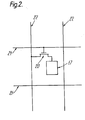
- Each pel pad 17 is connected to the drain of its associated FET 20 whose gate and source are respectively connected to the associated row and column access lines 21 and 22, appropriate to the position of that pel pad in the display matrix.
- the display is written line by line, with the data appropriate to each line being applied in turn to the column access lines (source lines) 22, while the row access lines (gate lines) 21 are strobed.
- Metal lines have the shortest risetimes (typical resistance is 0.03 ohms per square, and capacitance about 2 x 10 -5 Fm -2 ), polysilicon next (resistance 20-50 ohms per square, and capacitance about 5 x 10 5Fm 2). Diffusions have lower resistance (about 10 ohms per square), but higher capacitance (about 3.2 x 10 -4 Fm -2 ).
- the source lines generally require the shorter risetimes, particularly if the display addressing mode calls for all pels to be simultaneously blanked, and hence it is preferred to make them of metal throughout, and to make the gate lines of metal except at the crossovers, where diffusions are used.
- electrically insulating layers 16 and 18 have been provided in order to prevent the degradation of the liquid crystal layer by electrolytic effects, and therefore the pels must be driven by an alternating field.
- the voltage swing available from an NMOS silicon wafer is less than the peak-to-peak square wave voltage required to drive a conventional phase-change type liquid crystal layer in which the concentration of chiral additive is great enough to provide a cholesteric pitch significantly shorter than the liquid crystal layer thickness. This means that with this type of electro-optic effect it is necessary to apply an alternating voltage to the front electrode 15 in antiphase with that applied to the pads 17.
- Dyed nematic and dyed phase-change cells with minimal chiral additive providing a pitch equal to or greater than the liquid crystal layer thickness have the advantage that they can be driven by lower voltages permitting an addressing scheme in which the front electrode is held at a constant potential. This permits a relatively simple addressing scheme in which the pads 17 are driven positive with respect to the front electrode for one field of the input data video signal, and negative for the next. This is satisfactory provided that leakage effects do not give rise to excessive voltage droop between consecutive addressings of each pel.
- Figure 3 models a drive system in which the front electrode is held at a voltage V while the voltage applied to a fully 'ON' pad alternates between 2V and 0 volts. These voltages are applied to the pad by short duration pulses 30 that momentarily open the gate of the associated FET. The repetition frequency of these pulses is set by the video signal and is typically 50 Hz.
- Figure 3 depicts the situation where leakage provides a time constant that is short compared with the interval between consecutive pulses 30.
- the voltage waveform 31 of an ' . ON' pad is asymmetrical about the front electrode potential, and hence the integrity of the electrically insulating layers 16 and 18 is seen to be important.
- the voltage waveform 32 of an 'OFF' pad is also asymmetrical about the front electrode potential, and hence the 'OFF' pels see an unwanted residual drive waveform. If the time constant is the same for all pels across the whole display this problem can be simply resolved by choice of an appropriate offset voltage. In practice however, transistor leakage is generally found to vary significantly over the surface of a wafer, and hence this simple approach to the problem will not achieve the desired result in situations in which transistor leakage is the dominant factor determining the time constant.
- the time constant of a pel is governed by the capacitance between the pad 17 and the silicon wafer, and that between the pad and the front electrode.
- the associated leakage resistance is made up of the leakage resistance through the thickness of the liquid crystal layer and the leakage resistance of the transistor.
- the transistor leakage becomes significant in relation to the liquid crystal leakage, and at some pel size, typically below 100 microns square, the performance of the matrix starts to depend critically on the leakage resistance of the transistors. For this reason it is generally desirable to use a matrix whose pel pads 17 are at least as large as the possible consistent with the resolution requirements imposed by the particular application for which the cell is designed.
- One way of reducing the significance of variation in transistor leakage in displays with small pels is to adopt a drive scheme as depicted in Figure 4.
- the same voltages are used as have been described with reference to the Figure 3 drive scheme, but in this instance the waveform applied to the gate of the FET associated with the pad consists of a train of data pulses 40 interspersed with a succession of blanking pulses 41.
- the first blanking pulse occurs about a third of a frame period after the data pulse.
- the resulting 'ON' and 'OFF' voltage waveforms are depicted respectively by waveforms 42 and 43.
- a data pulse 50 opens the FET, and, in the case of a fully 'ON' pel causes the pad to be taken to the full voltage of 2V volts.
- a blanking pulse 51 restores the pad to 0 volts, producing the waveform 52. In this instance only one blanking pulse is required between each pair of consecutive data pulses.
- the data pulse for a fully 'OFF' pel keeps the voltage of the pad at 0 volts, and the blanking pulse leaves its voltage unchanged.
- FIG. 6 is a schematic of on-wafer circuitry used to reduce these connections to a manageable number. It will be seen that the source and gate lines of the matrix are each accessed by the circuitry from one end only, and hence it is possible to duplicate the access circuitry, using a mirror image layout around the two unused sides of the array. It will be appreciated that the display calls for the correct functioning of a very large number of active devices in the wafer, and this duplication provides a measure of redundancy that improves the manufacturing yield of acceptable wafers. A wafer with this redundancy may be tested before assembly to select which part of the access circuitry to use, and which to disable.
- the display is preferably specularly reflecting.
- the reflection is conveniently provided by the material of the pel pads 17, and it is found that conventional metallisation used in standard MOS technology provides acceptable reflecting properties, and hence in the manufacture of the wafer entirely standard MOS manufacturing processes are used right up to the provision of the molecular alignment treatment required for achieving the requisite orientation of the liquid crystal molecules at the adjacent surface of the liquid crystal layer 11.
- the cell When the cell has been assembled, it is vacumm filled via an aperture formed by a break (not shown) in the edge seal 12. Once the enclosure has been filled the aperture is sealed off with a suitable plug.
- a suitable liquid crystal filling is the nematic guest/host mixture marketed by BDH under the designation D86 (black dye) in host E63.
- D86 black dye
- CB15 cyano-biphenyl marketed by BDH under the designation CB15. Normally this will be added in a proportion that keeps the cholesteric pitch greater than "the thickness of the liquid crystal layer so as to avoid introducing excessive hysteresis in the optical transfer characteristic of the mixture.
Landscapes
- Physics & Mathematics (AREA)
- Nonlinear Science (AREA)
- Engineering & Computer Science (AREA)
- General Physics & Mathematics (AREA)
- Optics & Photonics (AREA)
- Crystallography & Structural Chemistry (AREA)
- Chemical & Material Sciences (AREA)
- Mathematical Physics (AREA)
- Theoretical Computer Science (AREA)
- Liquid Crystal (AREA)
- Microelectronics & Electronic Packaging (AREA)
- Liquid Crystal Display Device Control (AREA)
- Fax Reproducing Arrangements (AREA)
Applications Claiming Priority (2)
| Application Number | Priority Date | Filing Date | Title |
|---|---|---|---|
| GB08209710A GB2118347B (en) | 1982-04-01 | 1982-04-01 | Coherent light image generation |
| GB8209710 | 1982-04-01 |
Publications (1)
| Publication Number | Publication Date |
|---|---|
| EP0090987A1 true EP0090987A1 (de) | 1983-10-12 |
Family
ID=10529475
Family Applications (1)
| Application Number | Title | Priority Date | Filing Date |
|---|---|---|---|
| EP83102712A Withdrawn EP0090987A1 (de) | 1982-04-01 | 1983-03-18 | Erzeugung kohärenter optischer Bilder |
Country Status (3)
| Country | Link |
|---|---|
| EP (1) | EP0090987A1 (de) |
| JP (1) | JPH084308B2 (de) |
| GB (1) | GB2118347B (de) |
Cited By (1)
| Publication number | Priority date | Publication date | Assignee | Title |
|---|---|---|---|---|
| WO1999031646A1 (en) * | 1997-12-02 | 1999-06-24 | Eriksson Soeren | Display |
Families Citing this family (5)
| Publication number | Priority date | Publication date | Assignee | Title |
|---|---|---|---|---|
| GB2149554B (en) * | 1983-11-08 | 1987-04-01 | Standard Telephones Cables Ltd | Data terminals |
| JPS60120399A (ja) * | 1983-12-02 | 1985-06-27 | シチズン時計株式会社 | ダイオ−ド型表示装置の駆動方法 |
| GB2154331B (en) * | 1984-02-16 | 1987-07-01 | Standard Telephones Cables Ltd | Coherent light optical processor |
| US4772101A (en) * | 1986-11-07 | 1988-09-20 | The United States Of America As Represented By The Administrator Of The National Aeronautics And Space Administration | Remotely controllable real-time optical processor |
| JPS6410223A (en) * | 1987-07-02 | 1989-01-13 | Citizen Watch Co Ltd | Liquid crystal display panel |
Citations (6)
| Publication number | Priority date | Publication date | Assignee | Title |
|---|---|---|---|---|
| US3744879A (en) * | 1971-10-26 | 1973-07-10 | Hughes Aircraft Co | Liquid crystal optical processor |
| US4018509A (en) * | 1976-03-08 | 1977-04-19 | Hughes Aircraft Company | Optical data processing system with reflective liquid crystal light valve |
| DE2811290A1 (de) * | 1977-03-23 | 1978-09-28 | Westinghouse Electric Corp | Anzeigefeld |
| EP0014540A1 (de) * | 1979-01-24 | 1980-08-20 | Research Development Corporation National | Flüssigkristall-Anzeigevorrichtung zur Anzeige in Farbe |
| GB2042238A (en) * | 1979-02-14 | 1980-09-17 | Matsushita Electric Industrial Co Ltd | Drive circuit for a liquid crystal display panel |
| GB2066545A (en) * | 1979-12-27 | 1981-07-08 | Suwa Seikosha Kk | Liquid crystal display device |
Family Cites Families (2)
| Publication number | Priority date | Publication date | Assignee | Title |
|---|---|---|---|---|
| JPS5660494A (en) * | 1979-10-23 | 1981-05-25 | Tokyo Shibaura Electric Co | Projector type display unit |
| JPS5735924U (de) * | 1980-08-08 | 1982-02-25 |
-
1982
- 1982-04-01 GB GB08209710A patent/GB2118347B/en not_active Expired
-
1983
- 1983-03-18 EP EP83102712A patent/EP0090987A1/de not_active Withdrawn
- 1983-03-31 JP JP58056805A patent/JPH084308B2/ja not_active Expired - Lifetime
Patent Citations (6)
| Publication number | Priority date | Publication date | Assignee | Title |
|---|---|---|---|---|
| US3744879A (en) * | 1971-10-26 | 1973-07-10 | Hughes Aircraft Co | Liquid crystal optical processor |
| US4018509A (en) * | 1976-03-08 | 1977-04-19 | Hughes Aircraft Company | Optical data processing system with reflective liquid crystal light valve |
| DE2811290A1 (de) * | 1977-03-23 | 1978-09-28 | Westinghouse Electric Corp | Anzeigefeld |
| EP0014540A1 (de) * | 1979-01-24 | 1980-08-20 | Research Development Corporation National | Flüssigkristall-Anzeigevorrichtung zur Anzeige in Farbe |
| GB2042238A (en) * | 1979-02-14 | 1980-09-17 | Matsushita Electric Industrial Co Ltd | Drive circuit for a liquid crystal display panel |
| GB2066545A (en) * | 1979-12-27 | 1981-07-08 | Suwa Seikosha Kk | Liquid crystal display device |
Non-Patent Citations (2)
| Title |
|---|
| IEEE JOURNAL OF QUANTUM ELECTRONICS, vol. QE-15, no. 12, December 1979 B.D. GUENTHER et al. "Coherent Optical Processing Another Approach" pages 1348-1362 * |
| PROCEEDINGS OF THE SOCIETY OF PHOTO-OPTICAL INSTRUMENTATION ENGINEERS, vol. 231, 1980 1980 INTERNATIONAL OPTICAL COMPUTING CONFERENCE (Book I) J.G.DUTHIE et al. "Real-time optical correlation with solid--state sources" Pages 281-290 * |
Cited By (1)
| Publication number | Priority date | Publication date | Assignee | Title |
|---|---|---|---|---|
| WO1999031646A1 (en) * | 1997-12-02 | 1999-06-24 | Eriksson Soeren | Display |
Also Published As
| Publication number | Publication date |
|---|---|
| GB2118347A (en) | 1983-10-26 |
| JPH084308B2 (ja) | 1996-01-17 |
| GB2118347B (en) | 1985-06-19 |
| JPS5910928A (ja) | 1984-01-20 |
Similar Documents
| Publication | Publication Date | Title |
|---|---|---|
| EP0090988B1 (de) | Abtastung von Flüssigkristall-Anzeigeelementen | |
| US4574282A (en) | Coherent light image generation | |
| US5130830A (en) | Spatial light modulator and spatial light modulating apparatus with alignment film having particular conductance | |
| US4277145A (en) | Liquid-crystal display device | |
| GB2188471A (en) | L C D devices | |
| JPH04318514A (ja) | ポリマー分散液晶セルの動作用の成形された電圧パルス方法およびそれを使用した光バルブ | |
| US4036553A (en) | Method of controlling an optical characteristic | |
| US4807976A (en) | Light valve system and method with pulsed readout | |
| EP0090987A1 (de) | Erzeugung kohärenter optischer Bilder | |
| US5281806A (en) | Optical writing type liquid crystal light valve and writing apparatus therefor | |
| JP3165575B2 (ja) | 光情報装置の製造方法 | |
| EP0475249B1 (de) | Verfahren zur Steuerung eines lichtadressierten Flüssigkristallichtventils | |
| US4048628A (en) | Method and apparatus for erasing scattering in storage-type liquid crystals by frequency sweeping | |
| US7095405B2 (en) | Output control circuit, driving circuit, electro-optic apparatus, and electronic instrument | |
| US5040879A (en) | Variable density optical filter | |
| Flannery | Light-controlled light valves | |
| GB2113444A (en) | Matrix addressed liquid crystal displays | |
| Powles et al. | Enhancement of optically addressed liquid crystal SLM performance for specific applications by selection of input polarisation | |
| JPS6256931A (ja) | 投写型液晶表示装置 | |
| JP3289641B2 (ja) | 映像表示装置およびその駆動方法 | |
| US20240005984A1 (en) | A spatial light modulator | |
| JP2631457B2 (ja) | ライトバルブおよび投写型表示装置 | |
| JPH03200117A (ja) | 光学画像記憶装置の駆動方法 | |
| JPH04204828A (ja) | 液晶空間光変調素子および光学的画像処理装置 | |
| JPS60230637A (ja) | 液晶素子 |
Legal Events
| Date | Code | Title | Description |
|---|---|---|---|
| PUAI | Public reference made under article 153(3) epc to a published international application that has entered the european phase |
Free format text: ORIGINAL CODE: 0009012 |
|
| AK | Designated contracting states |
Designated state(s): CH DE FR IT LI NL |
|
| 17P | Request for examination filed |
Effective date: 19840321 |
|
| RAP1 | Party data changed (applicant data changed or rights of an application transferred) |
Owner name: STC PLC |
|
| 18D | Application deemed to be withdrawn |
Effective date: 19931001 |
|
| STAA | Information on the status of an ep patent application or granted ep patent |
Free format text: STATUS: THE APPLICATION IS DEEMED TO BE WITHDRAWN |
|
| R18D | Application deemed to be withdrawn (corrected) |
Effective date: 19870401 |
|
| APAF | Appeal reference modified |
Free format text: ORIGINAL CODE: EPIDOSCREFNE |
|
| RIN1 | Information on inventor provided before grant (corrected) |
Inventor name: ROSS, PETER WILLIAM Inventor name: CROSSLAND, WILLIAM ALDEN Inventor name: PETERS, JACK ROWLAND Inventor name: AYLIFFE, PETER JOHN |