EP0093868A2 - Elektronenstrahlröhre - Google Patents
Elektronenstrahlröhre Download PDFInfo
- Publication number
- EP0093868A2 EP0093868A2 EP83102957A EP83102957A EP0093868A2 EP 0093868 A2 EP0093868 A2 EP 0093868A2 EP 83102957 A EP83102957 A EP 83102957A EP 83102957 A EP83102957 A EP 83102957A EP 0093868 A2 EP0093868 A2 EP 0093868A2
- Authority
- EP
- European Patent Office
- Prior art keywords
- electron
- electron beam
- potential
- electrode
- generating
- Prior art date
- Legal status (The legal status is an assumption and is not a legal conclusion. Google has not performed a legal analysis and makes no representation as to the accuracy of the status listed.)
- Granted
Links
- 238000010894 electron beam technology Methods 0.000 title claims abstract description 83
- 230000003287 optical effect Effects 0.000 claims abstract description 26
- 230000000903 blocking effect Effects 0.000 claims 1
- 230000001133 acceleration Effects 0.000 description 14
- 238000012360 testing method Methods 0.000 description 4
- 239000000919 ceramic Substances 0.000 description 2
- 238000010276 construction Methods 0.000 description 1
- 230000000694 effects Effects 0.000 description 1
- 238000007689 inspection Methods 0.000 description 1
- 238000004519 manufacturing process Methods 0.000 description 1
- 238000000034 method Methods 0.000 description 1
- 238000004806 packaging method and process Methods 0.000 description 1
Images

Classifications
-
- H—ELECTRICITY
- H01—ELECTRIC ELEMENTS
- H01J—ELECTRIC DISCHARGE TUBES OR DISCHARGE LAMPS
- H01J37/00—Discharge tubes with provision for introducing objects or material to be exposed to the discharge, e.g. for the purpose of examination or processing thereof
- H01J37/02—Details
- H01J37/04—Arrangements of electrodes and associated parts for generating or controlling the discharge, e.g. electron-optical arrangement or ion-optical arrangement
-
- H—ELECTRICITY
- H01—ELECTRIC ELEMENTS
- H01J—ELECTRIC DISCHARGE TUBES OR DISCHARGE LAMPS
- H01J37/00—Discharge tubes with provision for introducing objects or material to be exposed to the discharge, e.g. for the purpose of examination or processing thereof
- H01J37/30—Electron-beam or ion-beam tubes for localised treatment of objects
- H01J37/3002—Details
- H01J37/3007—Electron or ion-optical systems
Definitions
- the invention relates to electron beam apparatus and is more particularly concerned with apparatus for producing in a common image plane an image alternatively from one or other of two electron beams having different electron potentials.
- IBM Technical Disclosure Bulletin article “Tri-Potential Method for Testing Electrical Opens and Shorts in Multilayer Ceramic Packaging Modules” (Vol.24, No.llA, April 1982 at pages 538890) describes a method of making a functional electrical test of a multilayer ceramic chip carrier using a scanning electron beam to address test points at two different electron potentials, one for charging and one for inspection. In order for this testing method to be practical, the electron beam potential must be switched between the two different electron potential values as quickly as possible.
- the field strengths of associated electron optical elements also must be increased at the same time so that the final focal plane of the electron beam does not move.
- all the variables necessary to switch an electron beam potential could be simultaneously changed by a control system.
- the field strengths of electron optical lenses can be changed only slowly in comparison with conventional electronic switching speeds.
- the field strength of a magnetic lens can be changed only by changing the current level in a coil having a large inductance. Accordingly, the speed at which the electron potential of an electron beam can be changed is ordinarily limited by the speed at which the field strengths of electron optical elements in the electron optical column can be changed.
- Still another object is to provide apparatus for switching the electron potential of an electron beam between different values without moving the final focal plane and without changing the field strengths of associated magnetic lenses in the electron optical column.
- this invention in which the electron potential of an electron beam is switched between different values without moving the focal plane by effectively changing the axial position of the electron source at the same time that the electron potential is changed.
- the effective change in axial position of the electron source exactly compensates for the altered effectiveness which magnetic lenses have upon an electron beam of altered electron potential such that the final focal plane remains at the same position without adjusting the field strength of any magnetic lens.
- the electron source is effectively moved by providing two or more sources of electrons at effectively different axial locations with respect to the electron optical column lenses.
- the electron potential of the electron beam is then changed by switching between the different sources of electrons.
- the electron source is provided with an acceleration electrode for quickly switching the electron potential between different values.
- the electron source also has a focusing electrode which acts to simultaneously change the virtual position of the electron source.
- the invention provides electron beam apparatus comprising means for generating alternatively two electron beams having different energies (electron potentials) and common means for focusing the two beams, characterised by the provision of means effective in operation of increasing the actual or apparent electron source (object) to image (focus) plane distance so that both beams are focussed by the common means in the same image plane.
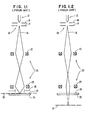
- FIG. 1.1 shows conventional electron beam apparatus, which includes an electron beam source 10 comprising a cathode or filament 12 for emitting electrons, an anode 14 for forming an electron beam 16 from emitted electrons, and a Wehnelt electrode 18 for limiting to a small area the region of cathode 12 from which electrons are extracted by anode 14 to form the electron beam 16.
- the electron beam 16 is focused upon a final focal plane 18' by an electron optical column 20 comprising magnetic lenses 22, 24 and deflection plates or coils 26.
- the velocity or energy (electron potential) of electrons within the beam is determined by the voltage potential through which the electrons are accelerated, which is the voltage difference between the anode and cathode (assuming the anode and target are at the same potential).
- the final focal plane 18' may be caused to coincide axially with the top surface 28 of a sample 30, as shown.
- FIG. 1.2 illustrates what happens in the prior art electron beam apparatus of FIG. 1.1 when the electron potential (energy of the electrons) of the beam is increased without changing the strengths of the magnetic lenses 22, 24.
- the electrons in beam 16 now have a higher velocity and are focused less by the magnetic lenses 22, 24.
- the focal plane 18 is axially displaced and no longer coincides with surface 28 of sample 30.
- the field strengths of lenses 22,24 also must be increased appropriately.
- To increase the strengths of magnetic lenses 22, 24 requires that the current levels in the associated coils be increased. These coils ordinarily have very high inductance so that the current cannot be changed very quickly in comparison with ordinary electronic switching speeds. This forms a limitation in the speed at which the electron beam potential can be switched.
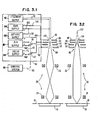
- FIG. 2 illustrates electron beam potential switching apparatus which avoids this limitation because the field strengths of lenses 22, 24 are not changed when the electron beam potential is switched to another value.
- the electron beam potential switching apparatus of this embodiment has more than one electron beam source.
- Two sources 32, 34 are illustrated but a higher number could be used instead to switch among a correspondingly larger number of beam potentials.
- Electron beam sources 32, 34 have cathodes 36, 38, Wehnelt electrodes 40, 42 and anodes 44, 46, all of which function in a conventional manner.
- Sources 32, 34 also have lenses 48, 50 for independently focusing the sources and deflection plates or coils 52, 54, for independently aligning the sources.
- focusing adjustment usually is done instead with one of the principle lenses 22, 24 of the associated electron optical column.
- Alignment adjustment is done by biasing additional alignment deflection plates (not shown) at the top of the electron optical column.
- beam selection apparatus 56 comprising deflection plates 58 and shield 60 having an aperture 62. Electron beam sources 32, 34 are oriented such that a first potential v 1 applied by switch 63 to plates 58 will deflect beam 64 from source 32 through aperture 62 and down column 20. At the same time, beam 66 from source 34 is deflected such that it does not pass through aperture 62. When a different second potential V 2 is applied to plates 58 by switch 63, beam 66 instead is deflected through aperture 62 and down column 20, while beam 64 is deflected such that it does not pass through aperture 62.
- beams 64, 66 have different beam potentials but are still focused at the same final focal plane 18 (when deflected down column 20 by selector 56). This is possible because the sources 32, 34 may be positioned physically at different axial distances from the electron optical column and/or because they may be independently focused by lenses 48, 50.
- beams 64, 66 may have a different number of cross- overs or intermediate focal points above the final focal plane 18.
- beam 64 has only one intermediate focal point 68 in addition to the electron gun cross-over 70, while beam 66 has two intermediate focal points 72, 74 in addition to the electron gun cross-over 76. It should be apparent from the much lesser deflection effect that lenses 22, 24 have upon beam 64 in comparison to beam 66 that beam 64 has a substantially higher beam potential.
- FIG. 3.1 Another electron beam switching apparatus in accordance with this invention is illustrated in FIG. 3.1 and comprises a pentode electron gun 80, a conventional electron optical column 20, a voltage switching circuit 82 for driving the pentode electron gun, and a control system 84, such as a computer for controlling the voltage switching circuit.
- the pentode electron gun 80 comprises a conventional filament or cathode 86, a conventional Wehnelt electrode 88, a conventional anode 90, an acceleration electrode 92, and a focusing electrode 94.
- Cathode 86, Wehnelt electrode 88 and anode 90 function just as in a conventional triode electron gun.
- Floating filament supply 96 powers a filament via lines 98 sufficiently that either the filament itself or a cathode heated by the filament emits electrons.
- Floating cathode supply 100 maintains a constant voltage V between the cathode 86 and anode 90 via lines 102.
- Floating bias supply 104 maintains a constant voltage difference between Wehnelt electrode 88 and cathode 86 via lines 106 and resistor 108.
- the voltages of the conventional parts of the pentode gun are adjustable, the relative voltages once adjusted are not switched to other values in this embodiment when the beam potential is switched, though the absolute voltages of these parts are floated and will change.
- the beam potential is changed by changing the voltage applied between accelerating electrode 92, and anode 90.
- the acceleration electrode 92 is maintained at the same potential as anode 90 for a first beam potential and the anode 90 is switched to a more negative potential than acceleration electrode 92 for a second (higher) beam potential. This is done by lowering the absolute potentials of the cathode, Wehnelt and anode with respect to the acceleration electrode 92.
- anode 90 is grounded through switch 110.
- the acceleration electrode 92 is always grounded so that it will remain at the same potential as the target. Otherwise there would be an additional electron acceleration or deceleration between the last pentode electrode 92 and the target (specimen 30).
- the focus electrode 94 is also grounded at the first beam potential via switch 112.
- switches 110 and 112 are simultaneously thrown by control system 84 via line 85 to the position not illustrated.
- the potential of anode 90 is thereby changed to a negative potential WV by supply 114.
- Cathode 86 and Wehnelt 88 are also floated automatically to lower absolute potentials by cathode supply 100 and bias supply 104.
- the voltage difference between anode 90 and the acceleration electrode 92 (WV) acts to increase the energy of electrons within the electron beam by a corresponding amount.
- focus supply 116 lowers the potential of focus electrode 94 via switch 112 and lines 118 to a value such that the focal plane 18 of the electron beam does not move.
- the beam configuration at the second (higher) beam potential is illustrated in FIG. 3.2. While the actual cross-over 120 of the electron beam source has not been moved very much (if any) by the acceleration and focusing electrodes, the trajectories of electrons emerging from the acceleration electrode at the second beam potential has been altered so that the electron beam at the higher second potential appears to have a virtual cross-over 122 farther away than at the first beam potential.
- the voltage switching circuit could be easily modified so that the acceleration and focusing electrodes may be switched each to any one of more than two voltage potentials in order to switch the beam potential among more than two values.
- the simultaneous aim of changing the total acceleration voltage and changing the focal characteristic such that the focal plane does not move could be implement with either more or less electrodes in an electron gun than the number illustrated.
- the electron beams at the two different beam potentials illustrated in FIGS. 3.1 and 3.2 also have a different number of cross-overs, just as in FIG. 2.
- the beams of different electron potential it is also possible for the beams of different electron potential to have the same number of cross-overs or intermediate focal points.
- a change in the number of cross-overs might be exactly compensated for by an appropriate change in beam potential, so that in such a limited case a change in actual position of the electron source would not be needed for the final focal plane to remain at the same position.
- This type of compensation (a change in the number of cross-overs) is optically equivalent to a large but fixed change in the effective axial location of the source and is regarded as such an equivalent by applicants.
- the difference in beam potentials usually desired will be sufficiently large that a change or switch in the number of beam cross-overs will be employed generally to make a large fixed switchable change in the effective source position and that other means for switchably adjusting the effective source position by a smaller amount will be used in combination therewith.
Landscapes
- Chemical & Material Sciences (AREA)
- Analytical Chemistry (AREA)
- Electron Sources, Ion Sources (AREA)
- Tests Of Electronic Circuits (AREA)
- Testing Or Measuring Of Semiconductors Or The Like (AREA)
- Testing Of Short-Circuits, Discontinuities, Leakage, Or Incorrect Line Connections (AREA)
Applications Claiming Priority (2)
| Application Number | Priority Date | Filing Date | Title |
|---|---|---|---|
| US376350 | 1982-05-10 | ||
| US06/376,350 US4426583A (en) | 1982-05-10 | 1982-05-10 | Electron beam potential switching apparatus |
Publications (3)
| Publication Number | Publication Date |
|---|---|
| EP0093868A2 true EP0093868A2 (de) | 1983-11-16 |
| EP0093868A3 EP0093868A3 (en) | 1986-07-16 |
| EP0093868B1 EP0093868B1 (de) | 1989-08-30 |
Family
ID=23484672
Family Applications (1)
| Application Number | Title | Priority Date | Filing Date |
|---|---|---|---|
| EP83102957A Expired EP0093868B1 (de) | 1982-05-10 | 1983-03-25 | Elektronenstrahlröhre |
Country Status (4)
| Country | Link |
|---|---|
| US (1) | US4426583A (de) |
| EP (1) | EP0093868B1 (de) |
| JP (1) | JPH0654640B2 (de) |
| DE (1) | DE3380504D1 (de) |
Cited By (2)
| Publication number | Priority date | Publication date | Assignee | Title |
|---|---|---|---|---|
| EP0150089A1 (de) * | 1984-01-19 | 1985-07-31 | Dubilier Plc | Optische System für geladene Teilchen |
| EP0161612A1 (de) * | 1984-05-18 | 1985-11-21 | Hitachi, Ltd. | Ionen-Mikrostrahl-Vorrichtung |
Families Citing this family (10)
| Publication number | Priority date | Publication date | Assignee | Title |
|---|---|---|---|---|
| JPS6196643A (ja) * | 1984-10-18 | 1986-05-15 | Fuji Photo Film Co Ltd | 透過型電子顕微鏡 |
| JPS61125126A (ja) * | 1984-11-22 | 1986-06-12 | Toshiba Mach Co Ltd | 電子ビ−ム露光装置 |
| JPH0654648B2 (ja) * | 1985-06-24 | 1994-07-20 | 日本電信電話株式会社 | パタン寸法測定方法 |
| US4855602A (en) * | 1986-06-20 | 1989-08-08 | Sharma Devendra N | Beam deflector |
| US4847502A (en) * | 1987-08-11 | 1989-07-11 | The United States Of America As Represented By The Administrator Of The National Aeronautics And Space Administration | Dual cathode system for electron beam instruments |
| EP1280180A3 (de) * | 2001-07-25 | 2005-02-09 | Lg.Philips Displays Korea Co., Ltd. | Elektronenkanone für Kathodenstrahlröhre |
| KR101376935B1 (ko) * | 2012-10-31 | 2014-03-20 | 삼성전기주식회사 | 비접촉식 전기검사장치 및 전기검사방법 |
| US10096447B1 (en) * | 2017-08-02 | 2018-10-09 | Kla-Tencor Corporation | Electron beam apparatus with high resolutions |
| CN114175206A (zh) * | 2019-07-26 | 2022-03-11 | Asml荷兰有限公司 | 多着陆能量扫描电子显微镜系统和方法 |
| CA3115634A1 (en) * | 2021-04-20 | 2022-10-20 | Rodney HERRING | Charged particle imaging system and use thereof |
Family Cites Families (7)
| Publication number | Priority date | Publication date | Assignee | Title |
|---|---|---|---|---|
| US3634645A (en) | 1970-04-21 | 1972-01-11 | Westinghouse Electric Corp | Work treating with electron beam |
| US3835327A (en) | 1972-05-08 | 1974-09-10 | United Aircraft Corp | Triode electron gun for electron beam machines |
| DE2234381C3 (de) * | 1972-07-10 | 1975-10-16 | Siemens Ag, 1000 Berlin Und 8000 Muenchen | Elektronenstrahl-Beleuchtungssystem |
| DE2338452A1 (de) * | 1973-07-28 | 1975-02-06 | Viktor Dr Ing Winkler | Verfahren und vorrichtung zur anregung und/oder bearbeitung von oberflaechen mit mehreren arten von korpuskularstrahlen in einem arbeitsgang sowie zur erzeugung und konzentration von korpuskularstrahlen |
| JPS5516321A (en) | 1978-07-21 | 1980-02-05 | Hitachi Ltd | Electrostatic radiant type electronic gun |
| JPS6057526B2 (ja) * | 1978-08-30 | 1985-12-16 | 大和製衡株式会社 | 体重計 |
| GB2081003B (en) * | 1980-07-28 | 1984-03-07 | Smith Kenneth C A | Microcircuit fabrication |
-
1982
- 1982-05-10 US US06/376,350 patent/US4426583A/en not_active Expired - Lifetime
-
1983
- 1983-03-18 JP JP58044615A patent/JPH0654640B2/ja not_active Expired - Lifetime
- 1983-03-25 EP EP83102957A patent/EP0093868B1/de not_active Expired
- 1983-03-25 DE DE8383102957T patent/DE3380504D1/de not_active Expired
Cited By (3)
| Publication number | Priority date | Publication date | Assignee | Title |
|---|---|---|---|---|
| EP0150089A1 (de) * | 1984-01-19 | 1985-07-31 | Dubilier Plc | Optische System für geladene Teilchen |
| EP0161612A1 (de) * | 1984-05-18 | 1985-11-21 | Hitachi, Ltd. | Ionen-Mikrostrahl-Vorrichtung |
| US4710632A (en) * | 1984-05-18 | 1987-12-01 | Hitachi, Ltd. | Ion microbeam apparatus |
Also Published As
| Publication number | Publication date |
|---|---|
| DE3380504D1 (en) | 1989-10-05 |
| JPH0654640B2 (ja) | 1994-07-20 |
| EP0093868A3 (en) | 1986-07-16 |
| JPS58201240A (ja) | 1983-11-24 |
| US4426583A (en) | 1984-01-17 |
| EP0093868B1 (de) | 1989-08-30 |
Similar Documents
| Publication | Publication Date | Title |
|---|---|---|
| US6444981B1 (en) | Scanning electron microscope | |
| US4426583A (en) | Electron beam potential switching apparatus | |
| US6194729B1 (en) | Particle beam apparatus | |
| US20150213998A1 (en) | Charged particle beam device with dynamic focus and method of operating thereof | |
| US8455838B2 (en) | Multiple-column electron beam apparatus and methods | |
| US5670782A (en) | Scanning electron microscope and speciman observation method thereby | |
| US5998795A (en) | Electron beam pattern-writing column | |
| EP0762468B1 (de) | Rasterelektronenmikroskop | |
| US4710639A (en) | Ion beam lithography system | |
| US4710632A (en) | Ion microbeam apparatus | |
| US4423305A (en) | Method and apparatus for controlling alignment of an electron beam of a variable shape | |
| US4868395A (en) | Electron beam lithography system for delineating a desired pattern on a target by means of electron beams | |
| US5668372A (en) | Scanning electron microscope and its analogous device | |
| US4893009A (en) | Scanning electron microscope and the like apparatus | |
| KR101010338B1 (ko) | 전자칼럼의 전자빔 에너지 변환 방법 | |
| EP0213664A1 (de) | In dünne Teilstrahlen aufgeteilter Strahl geladener Teilchen | |
| Thomson et al. | The EBES4 electron‐beam column | |
| EP0150941A1 (de) | Optische Systeme für geladene Teilchen | |
| Thomson | The electrostatic moving objective lens and optimized deflection systems for microcolumns | |
| JP3649008B2 (ja) | 電子線装置 | |
| US2274215A (en) | Electronic microscope | |
| JP3915812B2 (ja) | 電子線装置 | |
| JP3218467B2 (ja) | 荷電粒子線描画装置 | |
| JPS6264037A (ja) | 集束イオンビ−ム装置 | |
| JPS58129729A (ja) | テレビジヨン撮像管 |
Legal Events
| Date | Code | Title | Description |
|---|---|---|---|
| PUAI | Public reference made under article 153(3) epc to a published international application that has entered the european phase |
Free format text: ORIGINAL CODE: 0009012 |
|
| AK | Designated contracting states |
Designated state(s): DE FR GB IT |
|
| 17P | Request for examination filed |
Effective date: 19840320 |
|
| PUAL | Search report despatched |
Free format text: ORIGINAL CODE: 0009013 |
|
| AK | Designated contracting states |
Kind code of ref document: A3 Designated state(s): DE FR GB IT |
|
| 17Q | First examination report despatched |
Effective date: 19880728 |
|
| GRAA | (expected) grant |
Free format text: ORIGINAL CODE: 0009210 |
|
| AK | Designated contracting states |
Kind code of ref document: B1 Designated state(s): DE FR GB IT |
|
| REF | Corresponds to: |
Ref document number: 3380504 Country of ref document: DE Date of ref document: 19891005 |
|
| ITF | It: translation for a ep patent filed | ||
| ET | Fr: translation filed | ||
| PLBE | No opposition filed within time limit |
Free format text: ORIGINAL CODE: 0009261 |
|
| STAA | Information on the status of an ep patent application or granted ep patent |
Free format text: STATUS: NO OPPOSITION FILED WITHIN TIME LIMIT |
|
| 26N | No opposition filed | ||
| ITTA | It: last paid annual fee | ||
| PGFP | Annual fee paid to national office [announced via postgrant information from national office to epo] |
Ref country code: FR Payment date: 19950228 Year of fee payment: 13 |
|
| PGFP | Annual fee paid to national office [announced via postgrant information from national office to epo] |
Ref country code: DE Payment date: 19950330 Year of fee payment: 13 |
|
| PG25 | Lapsed in a contracting state [announced via postgrant information from national office to epo] |
Ref country code: FR Effective date: 19961129 |
|
| PG25 | Lapsed in a contracting state [announced via postgrant information from national office to epo] |
Ref country code: DE Effective date: 19961203 |
|
| REG | Reference to a national code |
Ref country code: FR Ref legal event code: ST |
|
| PGFP | Annual fee paid to national office [announced via postgrant information from national office to epo] |
Ref country code: GB Payment date: 19970224 Year of fee payment: 15 |
|
| PG25 | Lapsed in a contracting state [announced via postgrant information from national office to epo] |
Ref country code: GB Free format text: LAPSE BECAUSE OF NON-PAYMENT OF DUE FEES Effective date: 19980325 |
|
| GBPC | Gb: european patent ceased through non-payment of renewal fee |
Effective date: 19980325 |