EP0094224A1 - Photorécepteur - Google Patents
Photorécepteur Download PDFInfo
- Publication number
- EP0094224A1 EP0094224A1 EP83302579A EP83302579A EP0094224A1 EP 0094224 A1 EP0094224 A1 EP 0094224A1 EP 83302579 A EP83302579 A EP 83302579A EP 83302579 A EP83302579 A EP 83302579A EP 0094224 A1 EP0094224 A1 EP 0094224A1
- Authority
- EP
- European Patent Office
- Prior art keywords
- layer
- photoreceptor
- sic
- atomic percent
- hydrogen
- Prior art date
- Legal status (The legal status is an assumption and is not a legal conclusion. Google has not performed a legal analysis and makes no representation as to the accuracy of the status listed.)
- Granted
Links
Images


Classifications
-
- G—PHYSICS
- G03—PHOTOGRAPHY; CINEMATOGRAPHY; ANALOGOUS TECHNIQUES USING WAVES OTHER THAN OPTICAL WAVES; ELECTROGRAPHY; HOLOGRAPHY
- G03G—ELECTROGRAPHY; ELECTROPHOTOGRAPHY; MAGNETOGRAPHY
- G03G5/00—Recording-members for original recording by exposure, e.g. to light, to heat or to electrons; Manufacture thereof; Selection of materials therefor
- G03G5/02—Charge-receiving layers
- G03G5/04—Photoconductive layers; Charge-generation layers or charge-transporting layers; Additives therefor; Binders therefor
- G03G5/08—Photoconductive layers; Charge-generation layers or charge-transporting layers; Additives therefor; Binders therefor characterised by the photoconductive material being inorganic
- G03G5/082—Photoconductive layers; Charge-generation layers or charge-transporting layers; Additives therefor; Binders therefor characterised by the photoconductive material being inorganic and not being incorporated in a bonding material, e.g. vacuum deposited
- G03G5/08214—Silicon-based
- G03G5/08278—Depositing methods
-
- G—PHYSICS
- G03—PHOTOGRAPHY; CINEMATOGRAPHY; ANALOGOUS TECHNIQUES USING WAVES OTHER THAN OPTICAL WAVES; ELECTROGRAPHY; HOLOGRAPHY
- G03G—ELECTROGRAPHY; ELECTROPHOTOGRAPHY; MAGNETOGRAPHY
- G03G5/00—Recording-members for original recording by exposure, e.g. to light, to heat or to electrons; Manufacture thereof; Selection of materials therefor
- G03G5/02—Charge-receiving layers
- G03G5/04—Photoconductive layers; Charge-generation layers or charge-transporting layers; Additives therefor; Binders therefor
- G03G5/08—Photoconductive layers; Charge-generation layers or charge-transporting layers; Additives therefor; Binders therefor characterised by the photoconductive material being inorganic
- G03G5/082—Photoconductive layers; Charge-generation layers or charge-transporting layers; Additives therefor; Binders therefor characterised by the photoconductive material being inorganic and not being incorporated in a bonding material, e.g. vacuum deposited
- G03G5/08214—Silicon-based
- G03G5/08235—Silicon-based comprising three or four silicon-based layers
-
- H—ELECTRICITY
- H10—SEMICONDUCTOR DEVICES; ELECTRIC SOLID-STATE DEVICES NOT OTHERWISE PROVIDED FOR
- H10F—INORGANIC SEMICONDUCTOR DEVICES SENSITIVE TO INFRARED RADIATION, LIGHT, ELECTROMAGNETIC RADIATION OF SHORTER WAVELENGTH OR CORPUSCULAR RADIATION
- H10F71/00—Manufacture or treatment of devices covered by this subclass
- H10F71/10—Manufacture or treatment of devices covered by this subclass the devices comprising amorphous semiconductor material
- H10F71/103—Manufacture or treatment of devices covered by this subclass the devices comprising amorphous semiconductor material including only Group IV materials
- H10F71/1035—Manufacture or treatment of devices covered by this subclass the devices comprising amorphous semiconductor material including only Group IV materials having multiple Group IV elements, e.g. SiGe or SiC
-
- H—ELECTRICITY
- H10—SEMICONDUCTOR DEVICES; ELECTRIC SOLID-STATE DEVICES NOT OTHERWISE PROVIDED FOR
- H10F—INORGANIC SEMICONDUCTOR DEVICES SENSITIVE TO INFRARED RADIATION, LIGHT, ELECTROMAGNETIC RADIATION OF SHORTER WAVELENGTH OR CORPUSCULAR RADIATION
- H10F77/00—Constructional details of devices covered by this subclass
- H10F77/10—Semiconductor bodies
- H10F77/16—Material structures, e.g. crystalline structures, film structures or crystal plane orientations
- H10F77/162—Non-monocrystalline materials, e.g. semiconductor particles embedded in insulating materials
- H10F77/166—Amorphous semiconductors
- H10F77/1662—Amorphous semiconductors including only Group IV materials
- H10F77/1665—Amorphous semiconductors including only Group IV materials including Group IV-IV materials, e.g. SiGe or SiC
-
- Y—GENERAL TAGGING OF NEW TECHNOLOGICAL DEVELOPMENTS; GENERAL TAGGING OF CROSS-SECTIONAL TECHNOLOGIES SPANNING OVER SEVERAL SECTIONS OF THE IPC; TECHNICAL SUBJECTS COVERED BY FORMER USPC CROSS-REFERENCE ART COLLECTIONS [XRACs] AND DIGESTS
- Y02—TECHNOLOGIES OR APPLICATIONS FOR MITIGATION OR ADAPTATION AGAINST CLIMATE CHANGE
- Y02E—REDUCTION OF GREENHOUSE GAS [GHG] EMISSIONS, RELATED TO ENERGY GENERATION, TRANSMISSION OR DISTRIBUTION
- Y02E10/00—Energy generation through renewable energy sources
- Y02E10/50—Photovoltaic [PV] energy
- Y02E10/548—Amorphous silicon PV cells
-
- Y—GENERAL TAGGING OF NEW TECHNOLOGICAL DEVELOPMENTS; GENERAL TAGGING OF CROSS-SECTIONAL TECHNOLOGIES SPANNING OVER SEVERAL SECTIONS OF THE IPC; TECHNICAL SUBJECTS COVERED BY FORMER USPC CROSS-REFERENCE ART COLLECTIONS [XRACs] AND DIGESTS
- Y02—TECHNOLOGIES OR APPLICATIONS FOR MITIGATION OR ADAPTATION AGAINST CLIMATE CHANGE
- Y02P—CLIMATE CHANGE MITIGATION TECHNOLOGIES IN THE PRODUCTION OR PROCESSING OF GOODS
- Y02P70/00—Climate change mitigation technologies in the production process for final industrial or consumer products
- Y02P70/50—Manufacturing or production processes characterised by the final manufactured product
Definitions
- a photoreceptor A photoreceptor.
- the present invention relates to a photoreceptor, for example, an electrophotographic photoreceptor.
- the electrophotographic photoreceptor for example, the selenium photoreceptor or selenium photoreceptor doped with arsenic, tellurium, antimony, etc., or a photoreceptor with zinc oxide or cadmium sulfide dispersed in binder resin have so far been known.
- these photoreceptor pose problems of environmental pollution, thermal instability and insufficient mechanical strength.
- amorphous silicon (hereinafter abbreviated "a-Si") based electrophotographic photoreceptor has been proposed in recent years.
- the a-Si has so-called dangling bonds where the Si-Si bond is broken.
- This type of defects generate many localized energy levels in the energy gap. Therefore, there occurs hopping conduction of thermally excited carriers to lower the dark resistance while trapping of photo excited carriers by the localized energy levels results in poor photoconductivity. It is thus a practice to compensate these defects with hydrogen atoms, namely, to bond hydrogen atoms to silicon atoms to fill the dangling bonds.
- a-Si:H The above hydrogenated amorphous silicon (hereinafter called "a-Si:H”) exhibits a resistivity of 10 to 10 9 ohm-cm in the dark, which is about ten thousandth as low as the estimate with amorphous selenium. Therefore, the photoreceptor comprising a single layer of a-Si:H has such a problem that its surface potential decays in the dark at a high rate and its initial charging potential is low. On the other hand, for the sensitive layer of photoreceptor, this material has a very favorable characteristic that its resistivity decreases much when it is exposed to light of the visible or infra-red spectral region.
- a-Si:H With the potential retention, it can be doped with boron to increase its resistivity as high as 10 12 ohm-cm. However, it is not easy to control the boron doping level in a satisfactory accuracy. Further, a resistivity as high as 10 13 ohm-cm can be attained by introducing a trace of oxygen with boron. When used for the photoreceptor, however, this kind of material exhibits an inferior photosensitivity causing problems, such as unsharp potential drop at edge and nonnegligible residual potential . after exposure.
- the photoreceptor with a-Si:H exposed in surface has not yet been fully examined for the chemical stability of its surface, for example, possible effects of long-term exposure to atmosphere or moisture or those of chemical species as generated under corona discharges. It is known, however, that after having been left to stand for more than a month it is affected so much by moisture that there is a remarkable lowering in the charging potential.
- a-SiC:H hydrogenated amorphous silicon carbide
- An electrophotographic photoreceptor comprising a combination of a-SiC-Hand a-Si:H was proposed, for example, in the Japanese Patent Publication Open to Public Inspection (hereinafter called "Japanese Patent O.P.I. Publication) No. 17952/1982.
- a triple layered photoreceptor is formed wherein an a-Si:H layer provides a sensitive (photoconductive) layer with a first a-SiC:H layer formed on its light receiving surface and second a-SiC:H layer on its back surface (on substrate electrode side).
- an a-Si photoreceptor for example, for electrophotographic use that comprises a thin coating capable of retaining a high surface potential, exhibits superior sensitivity to light of the visible and infrared spectral ranges, high heat resistance and printing resistance, and yet stable resistances to environmental condition.
- the photoreceptor embodying the present invention comprises a photoconductive layer made of hydrogenated and/or fluorinated amorphous silicon, for example, a-Si:H, a surface modifying layer formed on such photoconductive layer and made of hydrogenated and/or fluorinated amorphous silicon carbide, for example, a-SiC:H, and a charge transport layer formed under the above photoconductive layer and made of hydrogenated and/or fluorinated amorphous silicon carbide, for example, a-SiC:H, preferably with insertion of a blocking layer made of hydrogenated and/or fluorinated amorphous silicon carbide, for example, a-SiC:H and doped with a high content of impurities, for example, phosphor or boron, to give a prescribed conduction type between the above charge transport layer and substrate, particularly substrate electrode, wherein the thickness "t" of the above surface 0 0 modifying layer is selected in a range 400A ⁇ t ⁇ 2000A
- a photoreceptor embodying the present invention will be described below in detail.
- This embodiment comprises, for example, as illustrated in Fig. 1, an electrically conductive substrate 1, and second a-SiC:H layer 2 (charge transport layer), a-Si:H layer 3 (photoconductive layer), and first a-SiC:H layer 4 (surface modifying layer) successively laminated on such substrate 1.
- the primary functions of the a-SiC:H layer 2 are to retain the given potential, transport charges and improve adherence of the coating to the substrate 1. It is o preferably formed 5,000 A to 80 ⁇ m thick and more preferably 10 ⁇ m to 30 ⁇ m.
- the photoconductive layer 3 generates charge carriers in response to impinging light, which is preferably formed 2,500 A to 5 ⁇ m and more preferably 1 ⁇ m to 2 ⁇ m thick.
- the first a-SiC:H layer 4 has functions to improve the surface potential characteristics of this photoreceptor, maintain its potential characteristics and resistance to the environmental condition (for avoidance of possible effects of moisture, atmosphere and chemical species produced by corona discharges) for a long period of time, improve its printing resistance through the high surface hardness, improve its hot transfer performance and particularly pressure intermediate transfer performance, etc.
- the layer 4 thus works, so to say, as the surface modifying layer. It is important to select the thickness "t" of this first a-SiC:H layer much smaller than the range of prior art, namely, in a 0 0 range of 400 A ⁇ t ⁇ 2,000 A as mentioned above. This point constitutes one of the indispensable requisites of the present invention.
- This a-SiC:H layer 4 is essential to improve the surface of photoreceptor in quality and thereby provide an a-Si photoreceptor excellent for practical use. Namely, it makes two basic properties of the electrophotographic photoreceptor, charge retention in the surface and the photo decay of surface potential available to the photoreceptor. The characteristic performances of the photoreceptor are thereby stabilized very much in repeated charging and photo decay, so even after the photoreceptor is left to stand for a long period, for example, longer than a month, its favorable potential characteristics can still be reproduced.
- the photoreceptor with a-Si:H-exposed in surface is liable to moisture, atmosphere, and air containing ozone, so its potential characteristics change much with time.
- a-SiC:H shows wearproof performances in copy process steps of development, image transfer, cleaning, etc. In addition, exhibiting favorable heat resistance, it can be applied to the hot process, for example, of pressure intermediate transfer.
- the thickness of the a-SiC:H layer 4 in the aforementioned range 0 of 400 A ⁇ t ⁇ 2,000 A. Namely, in case of thickness of 0 2,000 A or over, the residual potential level rises too high and further there is a decline in the sensitivity, resulting in the loss of favorable characteristics of the a-Si photoreceptor. On the other hand, in case of thickness 0 below 400 A, charges, as they deposit in the surface by charging, are lost by the tunnel effect, resulting in increased dark decay or remarkable decline in the photosensitivity. This is why it is essential to have the thickness of the a-SiC:H layer 4 0 selected in a range from 400 A to 2,000 A. Such thickness range can never be conceived of from the prior art, being discovered by the present author for the first time.
- the preferable ranye of x is from 0.1 to 0.9 (carbon content from 10 to 90 atomic percent), and more preferably, 0.1 to 0.7;
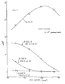
- the layer has an optical energy gap equivalent to about 2.0 eV or larger, so it only exhibitits reduced photoconductivity to visible and infrared spectral ranges as shown in Fig. 2 ( ⁇ D and ⁇ L are the resistivity in the dark and the one under exposure to light, respectively.
- the second a-SiC:H layer 2 is intended for two functions, charge retention and charge transport. It is characterized by a dark resistivity not smaller than 1 0 12 ohm-cm and a high withstand voltage and capable of retaining a high potential per unit thickness of layer. Further, electrons or holes injected from the sensitive layer 3 have a large mobility and life there, so charge carriers are efficiently transported to the substrate 1. In addition, since the energy gap can be adjusted properly by choosing the carbon content, it becomes possible to efficiently inject charge carriers from the sensitive layer 3 to the layer 2, as they are generated under exposure to light in the former layer, without presenting any barrier thereto.
- this second a-SiC:H layer 2 has such a merit that it exhibits a favorable performance in bonding or film adherence to the substrate 1, which is, for example, an aluminium electrode.
- the a-SiC:H layer 2 thus retains a high surface potential of practically usable level, transports charge carriers efficiently and fast as they are generated in the a-Si:H layer 3, and thereby provides a photoreceptor of high sensitivity practically free of residual potential.
- the a-SiC:H layer 2 preferably o has a thickness between 5,000 A and 80 ⁇ m and more preferably between 10 and 30 ⁇ m.
- a thickness below 5,000 A is too thin to achieve the surface potential level necessary for effective development, while at a thickness above 80 ⁇ m the surface potential increases excessively resulting not only in poor exfoliation of sticking toner but in adherence of carrier grains that comprise the double component developer.
- this a-SiC:H layer is made thin as compared to the selenium photoreceptor, for example, a little over 10 ⁇ m in thickness, a surface potential of practically usable level will still be attained.
- the preferable range of the parameter x is 0.1 ⁇ x ⁇ 0.9 (carbon content from 10 to 90 atomic percent).
- the layer 2 can be made completely different from the a-Si:H layer 3, while in case of x > 0.9, the layer 2 is almost fully composed of carbon losing the characteristic properties of semiconductor material and in addition the precipitation for coating takes more time.
- the preferable range is x ⁇ 0.9.
- a-Si:H layer photoconductive or sensitive layer
- This a-Si;H layer 3 exhibits a high photoconductivity to light of visible and infrared spectral regions. As illustrated in Fig. 2, red light of a wave length around 650 nm increases the ratio ⁇ D / ⁇ L to its maximum level of 10 4 in order. If this a-Si:H is used for the sensitive layer, a photoreceptor that is highly sensitive to the whole visible and infrared spectral regions can be provided.
- the a-Si:H layer 3 is 0 preferably 2,500 A to 5 ⁇ m thick.
- the impinging light is not fully absorbed by such layer, partially reaching the underlying a-SiC:H layer 2, which means a substantial decline in the photosensitivity.
- the a-Si:H layer 3 is endowed with a high charge transport capacity, it has a resistivity in the order of 10 9 ohm-cm exhibiting no charge retention in itself, so when it is used for the sensitive layer, it need not be thicker than the thickness necessary for the absorption of light. Thus, for its thickness, 5 ⁇ m is enough at maximum.
- This apparatus 11 has a vacuum chamber 12, in which the substrate 1 as mentioned above is held on the substrate holder 14 with a heater 15 built in to heat the substrate 1 to a prescribed temperature. Facing the substrate 1, there is disposed a high frequency electrode 17 to generate glow. discharges between itself and substrate 1.
- 20 through 24, 27 through 30, 35, 36, and 38 are valves, 31 is a source of SiH 4 or gaseous silicon compound, 32 is a source of CH 4 or gaseous carbon compound, 33 is a source of carrier gas, such as Ar or H 2 , and 34 is a source of 1% diborane or phosphine gas in argon.
- the substrate 1, for example, an aluminium plate is set in the vacuum chamber 12 after cleaning its surface.
- the valve 36 is then adjusted properly to evacuate the vacuum chamber 12 to a gas pressure of 10 -6 Torr and the substrate 1 is heated and maintained at a prescribed temperature, for example, 200°C.
- a gaseous mixture of SiH 4 or other gaseous silicon compound and CH 4 or other gaseous carbon compound diluted in a proper concentration with a carrier gas which is an inert gas of high purity is introduced in the vacuum chamber 12 and a high frequency voltage is applied from the high frequency power supply 16 under a reaction pressure of 0.01 to 10 Torr.
- the above reactant gases are thereby decomposed under glow discharges to deposit hydrogen containing a-SiC:H on the substrate 1 to form the layer 2 (and also the layer 4) as mentioned above.
- a-Si 1-x C x :H including one whose parameter x is, for example, as large as 0.9 can be deposited in a desirable composition with a desirable width of optical energy gap and at a rate 0 of 1,000 A/min or more without much changes in the electrical characteristics of deposited a-SiC:H.
- a-Si:H can be deposited for the above sensitive layer 3 by decomposing the silicon compound under glow discharges with no supply of the carbon compound.
- Both of the above first and second a-SiC:H layers must contain hydrogen since without loading of hydrogen, the photoreceptor will fail to exhibit charge retention characteristics satisfactory for practical application.
- the hydrogen content is preferably between 1 and 40 atomic percent and more preferably between 10 and 30 atomic percent.
- the hydrogen content of the photoconductive layer 3 is indispensable to compensate for the dangling bonds and thereby improve the photoconductivity and charge retention, which is ordinarily selected in a range from 1 to 40 atomic percent and preferably from 10 to 30 atomic percent.
- the hydrogen content of the photoconductive layer 3 is indispensable to compensate for the dangling bonds and thereby improve the photoconductivity and charge retention, which is ordinarily selected in a range from 1 to 40 atomic percent and preferably from 10 to 30 atomic percent.
- transition metals such as chromium and manganese
- a-Si (and a-SiC) can be loaded with fluorine instead of or in combination with hydrogen to provide a-Si:F or a-Si:H:F (and a-SiC:F or a-SiC:H:F).
- the fluorine content is preferably between 0.01 and 20 atomic percent and more preferably between 0.5 and 10 atomic percent.
- the above fabrication method uses the decomposition process under glow discharges.
- Beside, spattering, ion plating, or vaporization of a-si:H under presence of hydrogen activated or ionized by an hydrogen discharge tube and particularly by the present author's method as disclosed in Japanese Patent O.P.I. Publication No. 78413/1981 (Japanese Patent Application No. 152455/1979), etc. may be used in the fabrication of the photoreceptor as mentioned above.
- Beside SiH 4 and CH 4 , any of Si 2 H 6 , SiHF 3 , SiF 4 , and their gaseous derivatives and a gaseous lower hydrocarbon, such as C 2 H 6 or C 3 H 8 or CF 4 may be used for reactant gases.
- An electrophotographic photoreceptor having the layered structure of Fig. 1 was fabricated on an aluminium substrate by decomposition under glow discharges. To do this, first, a clean aluminium substrate with smooth surfaces was set in position in the vacuum reaction chamber of the glow discharger. After evacuation of the reaction chamber to a vacuum level as high as 10 -6 Torr, the substrate was heated to 200°C and then argon gas of high purity was introduced. A high frequency voltage of 13.56 MHz was applied under a back pressure of 0.5 Torr for a power density of 0.04 W/cm 2 to conduct preliminary discharges.
- Reactant gases, SiH 4 and CH 4 were then introduced to decompose a gas mixture of Ar + SiH 4 + CH 4 as supplied at a flow rate ratio of 2:1:1.5 under glow discharges.
- An a-SiC:H layer intended to retain the surface potential and transport charges was thus 0 prepared 1.0 ⁇ m thick at a deposition rate of 350 A/min.
- Optical energy gap of this a-Si:H layer was 2.1 eV. Further, by emans of Auger electron spectroscopy the carbon content was found to be 20 atomic percent.
- SiH 4 was decomposed under glow discharges with no supply of CH 4 using argon for the carrier gas to deposit the photoconductive a-Si:H layer 1.0 ⁇ m thick. Thereafter, the supply of CH 4 was resumed to decompose a gas mixture of Ar + SiH 4 + CH 4 as supplied this time at a different flow rate ratio of 2 : 1 : 4 to add a surface modifying a-SiC:H layer 0.15 ⁇ m thick. An electrophotographic photoreceptor was thus completed. The optical energy gap of this surface modifying a-SiC:H layer was estimated to be 2.5 eV. Further, an analysis showed that its carbon content was 50 atomic percent.
- a voltage of 6 kV of negative polarity was applied to the photoreceptor thus fabricated for corona discharges, when a surface potential of -85 V was attained. After dark decay of 6 sec, it changed to -60 V. Next, exposure to a beam of light of 1 lux resulted in an almost linear decay of the surface potential. At this time, the half-decay exposure was estimated to 0.5 lux-sec and there was detected almost no residual potential. Charging and exposure were repeated a hundred times, which proved very favorable repetition characteristics. On the other hand, though positive charging gave a surface potential and dark decay that were equivalent in degree to those estimated after negative charging, the photo dacay resulted in unsharp edge potential drop and a residual potential of 25 V.
- An electrophotographic photoreceptor of the layered structure that was achieved by the same method as in Example 1 except that the potential retention a-SiC:H layer next to the aluminium substrate was made 10 ⁇ m thick was fabricated, namely, by successively laminating such potential retention layer, a sensitive a-Si:H layer 1.0 ⁇ m thick and a surface modifying a-SiC:H layer 0.15 ⁇ m thick and its charging and photo decay characteristics were measured.
- a voltage of -6 kV was applied for corona discharges, the surface of photoreceptor was charged -750 V, which declined to -550 V after dark decay of 6 sec. Further, like Example 1, the photo decay characteristics under exposure to light and repetition characteristics were found very satisfactory.
- the Carlson's system was used with this photoreceptor to do negative charging under corona discharges, expose to the original image for formation of an electrostatic latent image, develop a visible image with positively charged toner through the magnetic brushing method and then transfer the visible image to the ordinary paper. There were thus successfully obtained sharp copy images of high density without background.
- Example 2 The same fabrication method as in Example 1 was used to form a potential retention a-SiC:H layer 10 ⁇ m thick on an aluminium substrate and further laminate a sensitive a-Si:H layer and a 0.15 ⁇ m thick surface a-SiC:H layer thereon.
- Photoreceptors whose sensitive a-Si:H layer was 0.1, 0.5 and 1.0 ⁇ m, respectively, were thus prepared. They were compared for the charging and photo decay characteristics. After being charged under corona discharges by application of a voltage of -6 kV, the surface of photoreceptor was exposed to a light of 1 lux.
- E1 ⁇ 2 was the half decay exposure (lux ⁇ sec) and V R was the residual potential (volt).
- V R was the residual potential (volt).
- the initial charging potential was -760 V in case the surface layer was 0.2 ⁇ m thick. For thicker surface layers, there were increases in the initial charging potential equivalent to differences in the residual potential in the above table.
- the surface a-SiC:H layer has the carbon content of 40 atomic percent or over as shown in Fig. 2 exhibiting practically no photoconductivity to visible and infrared spectra and therefore being transparent to these spectral ranges.
- photoreceptors having no surface a-Si:H layer were fabricated to examine their charging characteristics and resistance to environmental condition.
- a photoreceptor with an a-SiC:H layer next to the substrate being as thin as 0.5 to 1 ⁇ m and an a-SiC:H layer fabricated thereon as thick as 4 to 5 ⁇ m to form the free surface could be charged to 200 to 300 V in both polarities but there was a large dark decay and further its charging and photo decay characteristics changed much by repetition.
- a surface modifying a-SiC:H layer having a thickness in a particular range is indispensable to have an a-Si photoreceptor of practical, favorable and stable characteristics.
- the photoreceptor that conforms to this embodiment is formed, as illustrated in Fig. 5, on an electrically conductive substrate 1 by successively laminating a blocking layer 5 comprising n type or p type a-SiC:H doped with a high content of an element of the group VA or IIIA of the periodic table, and the already mentioned three layers, namely, the charge retention/transport a-SiC:H layer 2, photoconductive a-Si:H layer 3 and surface modifying a-SiC:H layer 4.
- the blocking layer 5 contributes much to prevent injection of carriers from the substrate 1 and thereby maintain the given surface potential satisfactorily.
- the layer may be of n type or further of n+ type in case of negative charging type photoreceptor and of p type or further of p+ type in case of positive charging type photoreceptor.
- Its thickness is preferably between 50 A to 1 ⁇ m and more preferably between 400 A to 1 ⁇ m.
- the second a-SiC:H layer is primarily intended for charge retention and transport, which is o preferably formed 5,000 A to 80 ⁇ m thick and more preferably 10to 30 ⁇ m thick.
- the photoconductive layer 3 generates charge carriers when exposed to light, which is preferably 0 formed 2,500 A to 10 ⁇ m thick and more preferably 2,500 A to 5 ⁇ m thick.
- the surface modifying layer 4 is intended to improve the surface potential characteristics of photoreceptor, maintain such characteristics for a long period of time, maintain the resistance to environmental condition for the prevention of possible effects of the moisture, atmosphere and chemical species as generated under corona discharges, improve the printing resistance by making use of a high surface hardness, and further improve the thermal resistance and hot transfer performance and particularly pressure intermediate transfer performance of the photoreceptor during its use.
- the thickness of this 0 surface modifying layer is 400 A or over but smaller than 0 2,000 A.
- the laminate structure of a-SiC:H/a-Si:H/a-SiC:H as already mentioned can be formed on the blocking layer, features of such laminate structure are provided while heavily doped with an element of the group VA or IIIA of the periodic table the blocking layer is converted into n type or p type, so on charging injection of carriers (holes or electrons) from the substrate may be effectively prevented.
- an a-Si photoreceptor for example, for electrophotographic use which, when compared to the conventional selenium photoreceptor, maintains a high potential at a thin coating thickness, exhibits superior sensitivity to light of visible and infrared spectral regions, presents high thermal resistance and printing resistance, and yet shows stable resistance to the environmental condition.
- the photoreceptor of the present embodiment can be fabricated by a glow discharger, apparatus as shown in Fig. 3. Namely, in this apparatus, first, a substrate 1, for example, an aluminium plate is set in position in a vacuum chamber 12 after cleaning its surface. Next, the chamber 12 is evacuated to a gas pressure of 10 -6 Torr by adjusting the valve 36 and the substrate 1 is heated and maintained at a prescribed temperature, for example, 200°C.
- a gas mixture of SiH 4 or gaseous silicon compound, phosphine or diborane gas, and CH 4 or gaseous carbon compound diluted to a proper concentration is introduced into the vacuum chamber 12 and a high frequency voltage is applied from the high frequency power supply 16 under a reaction pressure of 0.01 to 10 Torr.
- the above reactant gases are thereby decomposed under glow discharges to deposit a-SiC:H containing phosphorus or borone for formation of the above layer 5 on the substrate 1.
- the a-SiC:H layer 2, a-Si:H layer 3 and a-SiC:H layer 4 are formed in the way as already mentioned.
- the a-SiC:H layer 5 requires a proper selection of the flow rate ratio of the phosphine gas or diborane gas and gaseous silicon compound, for example, monosilane.
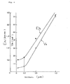
- Fig. 6 is a logarithmic plot of the dark resistance of the a-SiC:H layer 5 versus the flow rate ratio of phosphine PH 3 and monosilane SiH 4 as used in precipitation of such layer.
- Phosphorus doping with PH 3 lowers ⁇ D , which shows that a-SiC:H that is originally of n type is converted to the n+ type by a higher content of impurities resulting from such phosphorus doping. It was found that this provides a blocking layer that can satisfactorily prevent injection of carriers from the above mentioned substrate.
- the flow rate ratio of PH 3 /SiH 4 is preferably set to 100 to 10,000 ppm.
- Fig. 7 is a logarithmic plot of the dark resistance f of the a-SiC:H layer 5 versus the flow rate ratio of diborane and monosilane in case such layer is doped with an impurity of group IIIA.
- the undoped a-SiC:H exhibits a slight n type behavior in conductivity.
- the boron doping level is further increased with the flow rate ratio of B 2 H 6 /SiH 4 raised above 100 ppm, it is then transformed into the p type.
- the results in Fig. 4 show that if the flow rate ratio of B 2 H 6 /SiH 4 is selected properly to achieve the object of the invention, a-SiC:H can be converted into the p type and even into the p+ type as necessary.
- the doping level of phosphorus or boron of the a-SiC:H layer 5 must be selected properly, which, when expressed by the flow rate ratio of phosphine or diborone to silane (PH 3 /SiH 4 or B 2 H 6 /SiH 4 ), is preferably 100 to 10,000 ppm or 100 to 100,000 respectively.
- the photoreceptor conforming to the present embodiment comprises the a-SiC:H layer 5 that is converted into the n type or p type by impurity doping, a-SiC:H layer 2 and a-Si:H layer 3, so the combination of these layers cooperatively improves the surface potential retention, dark resistance, and further charging characteristics of the photoreceptor.
- this a-SiC:H layer 5 can be the same as the a-SiC:H layer 2 in the carbon and hydrogen contents and also the fluorine content in case of fluorination of such layer.
- Fig. 8 is an evaporation apparatus that is used to fabricate the photoreceptor embodying the present invention by the evaporation process.
- the bell jar 41 is connected to a vacuum pump (not shown) through an evacuation pipe 43 fitted with a butterfly valve 42.
- the inside of this bell jar 41 is thereby set to a high vacuum of 10 -3 to 10 Torr.
- a substrate 1 that is disposed in the bell jar 41 is heated by a heater 45 to 150 to 500°C and preferably to 250 to 450°C while a d.c. voltage of 0 to -10 kV and preferably -1 to -6 kV is applied from the d.c. power supply 46 to that substrate 1.
- a hydrogen gas discharge tube 47 opens into the vaccum chamber at a point opposite to the substrate 1, from which activated hydrogen and hydrogen ions are introduced into the bell jar 41.
- a silicon vapor source 48 and aluminium or antimony vapor source 49 that are disposed opposite to the substrate 1 are heated with each top shutter S open to simultaneously vaporize silicon and aluminium or antimony at an vaporization rate ratio, for example, of 1 : 0.01, Further, methane gas that is activated in a discharge tube 50 is introduced.
- a n+ type or p type a-SiC:H layer 5 (see Fig. 5) containing the prescribed content of aluminium or antimony is thus formed on the substrate 1.
- the a-SiC:H layers 2 and 4 can be deposited by stopping the vaporization of aluminium while the a-Si:H layer 3 can be deposited by stopping supply of aluminium or antimony and methane gas.
- the construction of the above discharge tubes 47 and 50 can be understood, for example, with reference to the former as illustrated in Fig. 9. It comprises an electrode member 62 of cylindrical form provided with a gas inlet 61, a discharge cavity 63 with such electrode member 62 disposed on one end, a discharge cavity member 64 enclosing such discharge cavity 63 and made, for example, a glass cylinder, and the other electrode member 66 of ring form disposed on the other end of such discharge cavity 63 and having an outlet 65.
- Application of a d.c. or a.c. voltage between the above two electrode members 62 and 66 starts glow discharges in the discharge cavity 63 filled with a gas, for example, hydrogen gas supplied from the gas inlet 61.
- the discharge cavity member 64 illustrated in Fig. 9 has a double tube construction to allow flow of cooling water which comes in from the cooling water inlet 67 and goes out from the cooling water outlet 68.
- the electrode member 62 is equipped with cooling fins 69. In the above hydrogen gas discharge tube, the electrode distance is 10 to 15 cm, the applied voltage is 600 V and the gas pressure in the discharge cavity 63 is set to about 10 -2 Torr.
- the a-SiC:H layer 5 is converted to the p type or n type by doping with aluminium or antimony.
- aluminium or antimony is preferably evaporated to a concentration of 100 to 10,000 ppm or 100 to 10,000 ppm respectively, in silicon vapors.
- An electrophotographic photoreceptor constructed as in Fig. 5 was fabricated on an aluminium substrate by the glow discharge process as follows. First, a clean aluminium substrate with smooth surfaces was installed in the vacuum reaction chamber of glow discharger. The reaction chamber was then evacuated to a high vacuum of 10 -6 Torr in order of magnitude. After the substrate was heated to 200°C, argon gas of high purity was introduced and under a back pressure of 0.5 Torr a high frequency voltage of 13.56 MHz was applied at a power density of 0.04 W/cm 2 for preliminary 15 min discharges. Next, a reactant gas comprising SiH 4 and CH 4 was introduced. As a gas mixture Ar + SiH 4 + CH 4 supplied at a flow rate ratio of 2 : 1 : 0.
- the surface 0 modifying layer was a 1500 A thick a-SiC:H layer
- the photoconductive layer was a 1 ⁇ m thick a-Si:H layer
- the potential retention layer was a 15 ⁇ m thick a-SiC:H layer containing 10 atomic percent of carbon atoms
- the substrate 0 was an aluminium plate
- the blocking layer was 2,000 A thick.
- V of the electrostatic characteristics was the initial charging potential
- ⁇ V/V was the percentage dark decay of potential 6 sec after completion of charging
- E1 ⁇ 2 was the half decay exposure (unit: lux ⁇ sec)
- V R was the residual potential.
Landscapes
- Chemical & Material Sciences (AREA)
- Inorganic Chemistry (AREA)
- Physics & Mathematics (AREA)
- General Physics & Mathematics (AREA)
- Photoreceptors In Electrophotography (AREA)
Applications Claiming Priority (4)
| Application Number | Priority Date | Filing Date | Title |
|---|---|---|---|
| JP57075658A JPS58192046A (ja) | 1982-05-06 | 1982-05-06 | 感光体 |
| JP75658/82 | 1982-05-06 | ||
| JP102418/82 | 1982-06-15 | ||
| JP57102418A JPS58219561A (ja) | 1982-06-15 | 1982-06-15 | 記録体 |
Publications (2)
| Publication Number | Publication Date |
|---|---|
| EP0094224A1 true EP0094224A1 (fr) | 1983-11-16 |
| EP0094224B1 EP0094224B1 (fr) | 1987-10-28 |
Family
ID=26416810
Family Applications (1)
| Application Number | Title | Priority Date | Filing Date |
|---|---|---|---|
| EP83302579A Expired EP0094224B1 (fr) | 1982-05-06 | 1983-05-06 | Photorécepteur |
Country Status (3)
| Country | Link |
|---|---|
| US (1) | US4510224A (fr) |
| EP (1) | EP0094224B1 (fr) |
| DE (1) | DE3374229D1 (fr) |
Cited By (5)
| Publication number | Priority date | Publication date | Assignee | Title |
|---|---|---|---|---|
| DE3616608A1 (de) * | 1985-05-17 | 1986-11-20 | Ricoh Co., Ltd., Tokio/Tokyo | Lichtempfindliches material fuer elektrophotographie |
| EP0211421A1 (fr) * | 1985-08-03 | 1987-02-25 | Matsushita Electric Industrial Co., Ltd. | Photorécepteur électrophotographique |
| US4687722A (en) * | 1983-08-03 | 1987-08-18 | Canon Kabushiki Kaisha | Image holder member with overlayer of amorphous Si with H and C |
| EP0250916A1 (fr) * | 1986-06-10 | 1988-01-07 | Minolta Camera Kabushiki Kaisha | Membre photosensible contenant une couche génératrice de charge et une couche transporteuse de charge et procédé de sa préparation |
| EP0187655A3 (fr) * | 1985-01-09 | 1988-12-14 | Hitachi, Ltd. | Dispositif photosensible électrophotograpique |
Families Citing this family (29)
| Publication number | Priority date | Publication date | Assignee | Title |
|---|---|---|---|---|
| JPS6012554A (ja) * | 1983-07-04 | 1985-01-22 | Fuji Photo Film Co Ltd | 電子写真用感光体 |
| AU549925B2 (en) * | 1983-11-28 | 1986-02-20 | Nitsuko Ltd. | Automatic telephone hold releasing circuit |
| JPS60119567A (ja) * | 1983-12-01 | 1985-06-27 | Ricoh Co Ltd | 電子写真感光体 |
| DE3511315A1 (de) * | 1984-03-28 | 1985-10-24 | Konishiroku Photo Industry Co., Ltd., Tokio/Tokyo | Elektrostatographisches, insbesondere elektrophotographisches aufzeichnungsmaterial |
| US4677044A (en) * | 1984-05-09 | 1987-06-30 | Konishiroku Photo Industry Co., Ltd. | Multi-layered electrophotographic photosensitive member having amorphous silicon |
| US4613556A (en) * | 1984-10-18 | 1986-09-23 | Xerox Corporation | Heterogeneous electrophotographic imaging members of amorphous silicon and silicon oxide |
| US4666803A (en) * | 1984-11-26 | 1987-05-19 | Kabushiki Kaisha Toshiba | Photoconductive member for exhibiting photoconductivity upon illumination by electromagnetic light in the visible to ultraviolet range |
| US4673629A (en) * | 1984-12-31 | 1987-06-16 | Konishiroku Photo Industry Co., Ltd. | Photoreceptor having amorphous silicon layers |
| US4743522A (en) * | 1985-09-13 | 1988-05-10 | Minolta Camera Kabushiki Kaisha | Photosensitive member with hydrogen-containing carbon layer |
| US5166018A (en) * | 1985-09-13 | 1992-11-24 | Minolta Camera Kabushiki Kaisha | Photosensitive member with hydrogen-containing carbon layer |
| US4738912A (en) * | 1985-09-13 | 1988-04-19 | Minolta Camera Kabushiki Kaisha | Photosensitive member having an amorphous carbon transport layer |
| US4741982A (en) * | 1985-09-13 | 1988-05-03 | Minolta Camera Kabushiki Kaisha | Photosensitive member having undercoat layer of amorphous carbon |
| US4749636A (en) * | 1985-09-13 | 1988-06-07 | Minolta Camera Kabushiki Kaisha | Photosensitive member with hydrogen-containing carbon layer |
| JPS62205361A (ja) * | 1986-03-05 | 1987-09-09 | Canon Inc | 電子写真用光受容部材及びその製造方法 |
| JPS62220959A (ja) * | 1986-03-20 | 1987-09-29 | Minolta Camera Co Ltd | 感光体 |
| JPS62220961A (ja) * | 1986-03-20 | 1987-09-29 | Minolta Camera Co Ltd | 感光体 |
| EP0238095A1 (fr) * | 1986-03-20 | 1987-09-23 | Minolta Camera Kabushiki Kaisha | Membre photosensible composé d'une couche transporteuse de charge et d'une couche génératrice de charge |
| JPS62223762A (ja) * | 1986-03-25 | 1987-10-01 | Canon Inc | 電子写真用光受容部材及びその製造方法 |
| EP0241032A3 (fr) * | 1986-04-09 | 1989-11-23 | Minolta Camera Kabushiki Kaisha | Elément photosensible composé d'une couche de transport de charges et d'une couche génératrice de charges |
| US4816324A (en) * | 1986-05-14 | 1989-03-28 | Atlantic Richfield Company | Flexible photovoltaic device |
| US4737429A (en) * | 1986-06-26 | 1988-04-12 | Xerox Corporation | Layered amorphous silicon imaging members |
| US4863821A (en) * | 1986-07-07 | 1989-09-05 | Minolta Camera Kabushiki Kaisha | Photosensitive member comprising charge generating layer and charge transporting layer having amorphous carbon |
| US4810606A (en) * | 1986-07-07 | 1989-03-07 | Minolta Camera Kabushiki Kaisha | Photosensitive member comprising charge generating layer and charge transporting layer |
| US4760005A (en) * | 1986-11-03 | 1988-07-26 | Xerox Corporation | Amorphous silicon imaging members with barrier layers |
| JPS63135949A (ja) * | 1986-11-26 | 1988-06-08 | Kyocera Corp | 電子写真感光体 |
| US5000831A (en) * | 1987-03-09 | 1991-03-19 | Minolta Camera Kabushiki Kaisha | Method of production of amorphous hydrogenated carbon layer |
| US5192631A (en) * | 1987-03-18 | 1993-03-09 | Dai Nippon Insatsu Kabushiki Kaisha | Variable electroconductivity material |
| US4906546A (en) * | 1988-05-14 | 1990-03-06 | Kyocera Corporation | Electrophotographic sensitive member |
| JP2962851B2 (ja) * | 1990-04-26 | 1999-10-12 | キヤノン株式会社 | 光受容部材 |
Citations (4)
| Publication number | Priority date | Publication date | Assignee | Title |
|---|---|---|---|---|
| FR2430097A1 (fr) * | 1978-06-26 | 1980-01-25 | Hitachi Ltd | Matiere photoconductrice |
| DE3040972A1 (de) * | 1979-10-30 | 1981-05-14 | Fuji Photo Film Co. Ltd., Minami-Ashigara, Kanagawa | Elektrophotographisches lichtempfindliches material und verfahren zu dessen herstellung |
| EP0029747A1 (fr) * | 1979-11-27 | 1981-06-03 | Konica Corporation | Installation pour le dépôt par vaporisation sous vide et procédé pour former une couche mince en utilisant cette installation |
| FR2490359A1 (fr) * | 1980-09-12 | 1982-03-19 | Canon Kk | Element photoconducteur |
Family Cites Families (2)
| Publication number | Priority date | Publication date | Assignee | Title |
|---|---|---|---|---|
| US4403026A (en) * | 1980-10-14 | 1983-09-06 | Canon Kabushiki Kaisha | Photoconductive member having an electrically insulating oxide layer |
| US4396793A (en) * | 1982-04-12 | 1983-08-02 | Chevron Research Company | Compensated amorphous silicon solar cell |
-
1983
- 1983-05-03 US US06/491,058 patent/US4510224A/en not_active Expired - Fee Related
- 1983-05-06 DE DE8383302579T patent/DE3374229D1/de not_active Expired
- 1983-05-06 EP EP83302579A patent/EP0094224B1/fr not_active Expired
Patent Citations (4)
| Publication number | Priority date | Publication date | Assignee | Title |
|---|---|---|---|---|
| FR2430097A1 (fr) * | 1978-06-26 | 1980-01-25 | Hitachi Ltd | Matiere photoconductrice |
| DE3040972A1 (de) * | 1979-10-30 | 1981-05-14 | Fuji Photo Film Co. Ltd., Minami-Ashigara, Kanagawa | Elektrophotographisches lichtempfindliches material und verfahren zu dessen herstellung |
| EP0029747A1 (fr) * | 1979-11-27 | 1981-06-03 | Konica Corporation | Installation pour le dépôt par vaporisation sous vide et procédé pour former une couche mince en utilisant cette installation |
| FR2490359A1 (fr) * | 1980-09-12 | 1982-03-19 | Canon Kk | Element photoconducteur |
Non-Patent Citations (2)
| Title |
|---|
| APPLIED PHYSICS LETTERS, vol. 39, no. 3, 1st August 1981, pages 237-239, New York, USA * |
| PATENTS ABSTRACTS OF JAPAN, vol. 6, no. 82, (P-116)[960], 20th May 1982 & JP - A - 57 17952 (OKI DENKI KOGYO K.K.) 29-01-1982 * |
Cited By (5)
| Publication number | Priority date | Publication date | Assignee | Title |
|---|---|---|---|---|
| US4687722A (en) * | 1983-08-03 | 1987-08-18 | Canon Kabushiki Kaisha | Image holder member with overlayer of amorphous Si with H and C |
| EP0187655A3 (fr) * | 1985-01-09 | 1988-12-14 | Hitachi, Ltd. | Dispositif photosensible électrophotograpique |
| DE3616608A1 (de) * | 1985-05-17 | 1986-11-20 | Ricoh Co., Ltd., Tokio/Tokyo | Lichtempfindliches material fuer elektrophotographie |
| EP0211421A1 (fr) * | 1985-08-03 | 1987-02-25 | Matsushita Electric Industrial Co., Ltd. | Photorécepteur électrophotographique |
| EP0250916A1 (fr) * | 1986-06-10 | 1988-01-07 | Minolta Camera Kabushiki Kaisha | Membre photosensible contenant une couche génératrice de charge et une couche transporteuse de charge et procédé de sa préparation |
Also Published As
| Publication number | Publication date |
|---|---|
| EP0094224B1 (fr) | 1987-10-28 |
| DE3374229D1 (en) | 1987-12-03 |
| US4510224A (en) | 1985-04-09 |
Similar Documents
| Publication | Publication Date | Title |
|---|---|---|
| US4510224A (en) | Electrophotographic photoreceptors having amorphous silicon photoconductors | |
| JPH0233146B2 (fr) | ||
| GB2099600A (en) | Photoconductive member | |
| US5510631A (en) | Non-monocrystalline silicon carbide semiconductor and semiconductor device employing the same | |
| US4794064A (en) | Amorphous silicon electrophotographic receptor having controlled carbon and boron contents | |
| JPH0373859B2 (fr) | ||
| US4859554A (en) | Multilayer photoreceptor | |
| JPS58219559A (ja) | 記録体 | |
| JPS6341059B2 (fr) | ||
| JPH0233148B2 (fr) | ||
| US5945241A (en) | Light receiving member for electrophotography and fabrication process thereof | |
| JPH0233144B2 (ja) | Denshishashinkankotai | |
| US6632578B2 (en) | Electrophotographic light-receiving member and process for its production | |
| JPH0233145B2 (ja) | Denshishashinkankotai | |
| US4585720A (en) | Photoconductive member having light receiving layer of a-(Si-Ge) and C | |
| US4579798A (en) | Amorphous silicon and germanium photoconductive member containing carbon | |
| JPH0234020B2 (ja) | Denshishashinkankotai | |
| JPH0225175B2 (fr) | ||
| JPS58219561A (ja) | 記録体 | |
| JPS6335979B2 (fr) | ||
| JPS5967551A (ja) | 記録体 | |
| JPS6341060B2 (fr) | ||
| JPS6314164A (ja) | 電子写真感光体 | |
| JPH0256662B2 (fr) | ||
| JPS60235151A (ja) | 感光体 |
Legal Events
| Date | Code | Title | Description |
|---|---|---|---|
| PUAI | Public reference made under article 153(3) epc to a published international application that has entered the european phase |
Free format text: ORIGINAL CODE: 0009012 |
|
| AK | Designated contracting states |
Designated state(s): DE GB |
|
| 17P | Request for examination filed |
Effective date: 19840508 |
|
| GRAA | (expected) grant |
Free format text: ORIGINAL CODE: 0009210 |
|
| AK | Designated contracting states |
Kind code of ref document: B1 Designated state(s): DE GB |
|
| REF | Corresponds to: |
Ref document number: 3374229 Country of ref document: DE Date of ref document: 19871203 |
|
| PLBE | No opposition filed within time limit |
Free format text: ORIGINAL CODE: 0009261 |
|
| STAA | Information on the status of an ep patent application or granted ep patent |
Free format text: STATUS: NO OPPOSITION FILED WITHIN TIME LIMIT |
|
| 26N | No opposition filed | ||
| PGFP | Annual fee paid to national office [announced via postgrant information from national office to epo] |
Ref country code: GB Payment date: 19920424 Year of fee payment: 10 |
|
| PGFP | Annual fee paid to national office [announced via postgrant information from national office to epo] |
Ref country code: DE Payment date: 19920529 Year of fee payment: 10 |
|
| PG25 | Lapsed in a contracting state [announced via postgrant information from national office to epo] |
Ref country code: GB Effective date: 19930506 |
|
| GBPC | Gb: european patent ceased through non-payment of renewal fee |
Effective date: 19930506 |
|
| PG25 | Lapsed in a contracting state [announced via postgrant information from national office to epo] |
Ref country code: DE Effective date: 19940201 |