EP0094708B1 - Mit Hilfe von Glas verkitteter Magnetkopf und Verfahren zu dessen Herstellung - Google Patents
Mit Hilfe von Glas verkitteter Magnetkopf und Verfahren zu dessen Herstellung Download PDFInfo
- Publication number
- EP0094708B1 EP0094708B1 EP83200650A EP83200650A EP0094708B1 EP 0094708 B1 EP0094708 B1 EP 0094708B1 EP 83200650 A EP83200650 A EP 83200650A EP 83200650 A EP83200650 A EP 83200650A EP 0094708 B1 EP0094708 B1 EP 0094708B1
- Authority
- EP
- European Patent Office
- Prior art keywords
- layer
- magnetic head
- glass
- sputtering
- gap
- Prior art date
- Legal status (The legal status is an assumption and is not a legal conclusion. Google has not performed a legal analysis and makes no representation as to the accuracy of the status listed.)
- Expired
Links
- 238000004519 manufacturing process Methods 0.000 title claims description 7
- 229910052581 Si3N4 Inorganic materials 0.000 claims abstract description 24
- VYPSYNLAJGMNEJ-UHFFFAOYSA-N Silicium dioxide Chemical compound O=[Si]=O VYPSYNLAJGMNEJ-UHFFFAOYSA-N 0.000 claims abstract description 22
- 238000009792 diffusion process Methods 0.000 claims abstract description 18
- 230000004888 barrier function Effects 0.000 claims abstract description 16
- 239000000463 material Substances 0.000 claims abstract description 16
- 238000000034 method Methods 0.000 claims abstract description 14
- HQVNEWCFYHHQES-UHFFFAOYSA-N silicon nitride Chemical compound N12[Si]34N5[Si]62N3[Si]51N64 HQVNEWCFYHHQES-UHFFFAOYSA-N 0.000 claims abstract description 9
- 229910052814 silicon oxide Inorganic materials 0.000 claims abstract description 8
- 238000004544 sputter deposition Methods 0.000 claims description 14
- IJGRMHOSHXDMSA-UHFFFAOYSA-N Atomic nitrogen Chemical compound N#N IJGRMHOSHXDMSA-UHFFFAOYSA-N 0.000 claims description 6
- 239000007789 gas Substances 0.000 claims description 6
- QVGXLLKOCUKJST-UHFFFAOYSA-N atomic oxygen Chemical compound [O] QVGXLLKOCUKJST-UHFFFAOYSA-N 0.000 claims description 5
- 239000001301 oxygen Substances 0.000 claims description 5
- 229910052760 oxygen Inorganic materials 0.000 claims description 5
- 229910052757 nitrogen Inorganic materials 0.000 claims description 3
- QJGQUHMNIGDVPM-UHFFFAOYSA-N nitrogen group Chemical group [N] QJGQUHMNIGDVPM-UHFFFAOYSA-N 0.000 claims description 3
- 239000000696 magnetic material Substances 0.000 claims description 2
- 238000007669 thermal treatment Methods 0.000 claims description 2
- 239000011521 glass Substances 0.000 abstract description 20
- 229910000859 α-Fe Inorganic materials 0.000 abstract description 18
- 238000010438 heat treatment Methods 0.000 description 3
- 239000000203 mixture Substances 0.000 description 3
- XUIMIQQOPSSXEZ-UHFFFAOYSA-N Silicon Chemical compound [Si] XUIMIQQOPSSXEZ-UHFFFAOYSA-N 0.000 description 2
- 239000000853 adhesive Substances 0.000 description 2
- 230000001070 adhesive effect Effects 0.000 description 2
- 238000010276 construction Methods 0.000 description 2
- 238000001816 cooling Methods 0.000 description 2
- 238000000151 deposition Methods 0.000 description 2
- 229910052710 silicon Inorganic materials 0.000 description 2
- 239000010703 silicon Substances 0.000 description 2
- 241000167854 Bourreria succulenta Species 0.000 description 1
- XMIJDTGORVPYLW-UHFFFAOYSA-N [SiH2] Chemical compound [SiH2] XMIJDTGORVPYLW-UHFFFAOYSA-N 0.000 description 1
- -1 borides Chemical class 0.000 description 1
- 230000007423 decrease Effects 0.000 description 1
- 230000008021 deposition Effects 0.000 description 1
- 238000005516 engineering process Methods 0.000 description 1
- 229910052751 metal Inorganic materials 0.000 description 1
- 239000002184 metal Substances 0.000 description 1
- 229910044991 metal oxide Inorganic materials 0.000 description 1
- 150000004706 metal oxides Chemical class 0.000 description 1
- 150000002739 metals Chemical class 0.000 description 1
- 150000004767 nitrides Chemical class 0.000 description 1
- RJCRUVXAWQRZKQ-UHFFFAOYSA-N oxosilicon;silicon Chemical compound [Si].[Si]=O RJCRUVXAWQRZKQ-UHFFFAOYSA-N 0.000 description 1
- 239000007858 starting material Substances 0.000 description 1
- 239000000126 substance Substances 0.000 description 1
- 238000004804 winding Methods 0.000 description 1
Images
Classifications
-
- G—PHYSICS
- G11—INFORMATION STORAGE
- G11B—INFORMATION STORAGE BASED ON RELATIVE MOVEMENT BETWEEN RECORD CARRIER AND TRANSDUCER
- G11B5/00—Recording by magnetisation or demagnetisation of a record carrier; Reproducing by magnetic means; Record carriers therefor
- G11B5/127—Structure or manufacture of heads, e.g. inductive
- G11B5/187—Structure or manufacture of the surface of the head in physical contact with, or immediately adjacent to the recording medium; Pole pieces; Gap features
- G11B5/23—Gap features
- G11B5/235—Selection of material for gap filler
-
- G—PHYSICS
- G11—INFORMATION STORAGE
- G11B—INFORMATION STORAGE BASED ON RELATIVE MOVEMENT BETWEEN RECORD CARRIER AND TRANSDUCER
- G11B5/00—Recording by magnetisation or demagnetisation of a record carrier; Reproducing by magnetic means; Record carriers therefor
- G11B5/127—Structure or manufacture of heads, e.g. inductive
- G11B5/187—Structure or manufacture of the surface of the head in physical contact with, or immediately adjacent to the recording medium; Pole pieces; Gap features
- G11B5/23—Gap features
- G11B5/232—Manufacture of gap
-
- Y—GENERAL TAGGING OF NEW TECHNOLOGICAL DEVELOPMENTS; GENERAL TAGGING OF CROSS-SECTIONAL TECHNOLOGIES SPANNING OVER SEVERAL SECTIONS OF THE IPC; TECHNICAL SUBJECTS COVERED BY FORMER USPC CROSS-REFERENCE ART COLLECTIONS [XRACs] AND DIGESTS
- Y10—TECHNICAL SUBJECTS COVERED BY FORMER USPC
- Y10T—TECHNICAL SUBJECTS COVERED BY FORMER US CLASSIFICATION
- Y10T29/00—Metal working
- Y10T29/49—Method of mechanical manufacture
- Y10T29/49002—Electrical device making
- Y10T29/4902—Electromagnet, transformer or inductor
- Y10T29/49021—Magnetic recording reproducing transducer [e.g., tape head, core, etc.]
- Y10T29/49032—Fabricating head structure or component thereof
- Y10T29/49036—Fabricating head structure or component thereof including measuring or testing
- Y10T29/49039—Fabricating head structure or component thereof including measuring or testing with dual gap materials
-
- Y—GENERAL TAGGING OF NEW TECHNOLOGICAL DEVELOPMENTS; GENERAL TAGGING OF CROSS-SECTIONAL TECHNOLOGIES SPANNING OVER SEVERAL SECTIONS OF THE IPC; TECHNICAL SUBJECTS COVERED BY FORMER USPC CROSS-REFERENCE ART COLLECTIONS [XRACs] AND DIGESTS
- Y10—TECHNICAL SUBJECTS COVERED BY FORMER USPC
- Y10T—TECHNICAL SUBJECTS COVERED BY FORMER US CLASSIFICATION
- Y10T29/00—Metal working
- Y10T29/49—Method of mechanical manufacture
- Y10T29/49002—Electrical device making
- Y10T29/4902—Electromagnet, transformer or inductor
- Y10T29/49021—Magnetic recording reproducing transducer [e.g., tape head, core, etc.]
- Y10T29/49032—Fabricating head structure or component thereof
- Y10T29/49048—Machining magnetic material [e.g., grinding, etching, polishing]
-
- Y—GENERAL TAGGING OF NEW TECHNOLOGICAL DEVELOPMENTS; GENERAL TAGGING OF CROSS-SECTIONAL TECHNOLOGIES SPANNING OVER SEVERAL SECTIONS OF THE IPC; TECHNICAL SUBJECTS COVERED BY FORMER USPC CROSS-REFERENCE ART COLLECTIONS [XRACs] AND DIGESTS
- Y10—TECHNICAL SUBJECTS COVERED BY FORMER USPC
- Y10T—TECHNICAL SUBJECTS COVERED BY FORMER US CLASSIFICATION
- Y10T29/00—Metal working
- Y10T29/49—Method of mechanical manufacture
- Y10T29/49002—Electrical device making
- Y10T29/4902—Electromagnet, transformer or inductor
- Y10T29/49021—Magnetic recording reproducing transducer [e.g., tape head, core, etc.]
- Y10T29/49032—Fabricating head structure or component thereof
- Y10T29/49055—Fabricating head structure or component thereof with bond/laminating preformed parts, at least two magnetic
- Y10T29/49057—Using glass bonding material
Definitions
- the invention relates to a magnetic head having a layer of non-magnetizable bonding material in the gap-forming area of a pair of magnet core parts, in which diffusion barriers are provided between the core parts and the layer of non-magnetizable material, and to a method of manufacturing such a magnetic head.
- Magnetic heads serve to record playback and/or erase magnetic information. They are used, for example, in tape recorders for recording and/or playing back audio information or video information. In particular when a magnetic head is used in tape recorders for recording and/or playing back video information (so-called video recorders) it is usual to manufacture the core of the magnetic head from (monocrystalline) ferrite.
- the gap of a magnetic head for a video recorder is formed by bonding two parts of (monocrystalline) ferrite to each other by means of a sputtered film of a low-melting-point glass.
- the ferrite is first coated with a layer which is impervious to glass and which is often termed the diffusion barrier.
- a diffusion barrier non-magnetizable metals, metal oxides, borides, nitrides, sillconoxide and ferrite which is non-magnetizable at room temperature
- a sputtered Si0 2 layer has so far been used in practice as a diffusion barrier.
- the glass becomes less and less viscous.
- the glass may work as an adhesive.
- a Si0 2 -layer dissolves in the glass.
- the glass becomes more viscous so that its value as an adhesive decreases.
- heating to 700 ⁇ 5°C has to be done quickly (in approximately 10 minutes) so as to obtain a good bonding. It has been found difficult to maintain this narrow tolerance of ⁇ 5°C.
- the damage to the Si 3 N 4 layer is probably the result of the high elastic stress at the interface Si 3 N 4 -ferrite. This stress may substantially be ascribed to the comparatively low elasticity of Si 3 N 4 .
- each diffusion barrier is composed of a layer of silicon nitride adjoining the non-magnetizable bonding layer, and a layer of silicon oxide.
- the invention also relates to a method of manufacturing a magnetic head having the above-mentioned structure.
- This method comprises the following steps: forming a first core part and a second core part of magnetic material; working a face of each of said core parts in such manner that said faces may serve as gap-forming faces; sputtering a layer of anti-diffusion material on each of the gap-forming faces; providing a layer of bonding material on at least one of the layers of anti-diffusion material; placing the two core parts against each other with the provided layers in between; and forming a permanent bond by means of a thermal treatment, and is characterized by sputtering a layer of Si0 2 having a desired thickness and by subsequently sputtering a layer of Si 3 N 4 having a desired thickness.
- the layer of Si 3 N 4 may be sputtered from an Si 3 N 4 target or, which is easier, may be sputtered in a nitrogen-containing gas atmosphere from a silicon target.
- the silicon target may be also used to sputter the layer of Si0 2 .
- sputtering should be carried out in an oxygen-containing atmosphere.
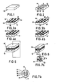
- a block of material 10 which may be manufactured from polycrystalline (sintered) or in particular monocrystalline ferrite (Fig. 1) is given the shape shown in Fig. 2 by means of the usual techniques. As is shown in Fig. 2, two grooves 14 and 16 are provided in the block and the surfaces 18, 20 and 22 are polished so that they may serve as gap-bounding faces.
- first layers 24 are provided on the surfaces 18, 20, 22 of core parts 10 and 10' (Fig. 3a, 3b). These first layers 24 consist of a non-magnetizable material which does not react, or at most reacts very slightly, with ferrite, in this case silicon oxide. This can easily be provided by means of a sputtering method and due to its comparatively high elasticity after providing shows a comparatively low elastic stress at the interface with the ferrite.
- An alternative method of providing a thin layer of Si0 2 is that of the so-called reactive vapour deposition. In this method a mixture of SiH 2 and 0 2 is applied to a furnace which is kept at a temperature of approximately 400°C and in which the pole pieces are present. It has been found that a homogeneous layer of Si0 2 is formed on the core parts.
- Second layers 26 are provided on the first layers 24.
- Said second layers 26 consist of Si 3 N 4 . Thickness between 100 and 1000 A are considered for the layers 24 and 26, 200 A being a characteristic thickness.
- the Si0 2 may be sputtered from an Si-target (in oxygen) instead of from an Si0 2 -target and the atmosphere during sputtering may then be replaced gradually by nitrogen as a result of which the last sputtered material becomes Si 3 N 4 .
- Bonding layers 28 are provided on the second layers 26 which together with the layers 24 form a diffusion barrier (Fig. 4a, 4b).
- These third layers 28 may consist of a glass which comprises 12-20% by weight of A1 2 0 3 , 40-48% by weight of B 2 0 3 and furthermore a share of one or more of the oxides BaO, CaO or SrO.
- a suitable glass comprises, for example, 15 mol % A1 2 0 3 , 60 mol % B 2 0 3 and 25 mol % BaO or SrO. This glass can be provided by means of sputtering with the composition remaining constant and can be provided in the same sputtering device as the layers 24, 26 from a glass target.
- the sum of the thicknesses of the layers 24, 26 and 28 determines the ultimate gap length of the magnetic head.
- the core parts 10, 10' are then placed against each other with the glass layers (Fig. 5) and heated in a furnace at a temperature which is sufficiently high to soften the layer of glass (for example, approximately 650°C), the core parts 10, 10' being pressed against each other at a pressure of 20-70 kg/cm 2 .
- the core parts 10, 10' are rigidly connected together and may then be further processed to obtain a magnetic head of the desired shape.
- the assembly may be processed and polished so that, with simultaneous adjustment of the gap height h, the construction shown in Fig. 6 is formed which has a tape contact face 29.
- this' construction may again be divided into individual magnet core segments 30 which after providing an electric winding 31 form a magnetic head 32.
- Fig. 7b shows, with reference to an enlargement of the gap-forming area of the magnetic head 32 of Fig. 7a, the resulting layer structure of the gap-forming area between the (ferrite) core parts 10 and 10'.
- a layer 24 of silicon oxide and a layer 26 of silicon nitride are provided on each of the core parts 10, 10'.
- the assembly is cemented together via a glass layer -28.
Landscapes
- Engineering & Computer Science (AREA)
- Manufacturing & Machinery (AREA)
- Magnetic Heads (AREA)
Claims (7)
Priority Applications (1)
| Application Number | Priority Date | Filing Date | Title |
|---|---|---|---|
| AT83200650T ATE21293T1 (de) | 1982-05-19 | 1983-05-06 | Mit hilfe von glas verkitteter magnetkopf und verfahren zu dessen herstellung. |
Applications Claiming Priority (2)
| Application Number | Priority Date | Filing Date | Title |
|---|---|---|---|
| NL8202059 | 1982-05-19 | ||
| NL8202059A NL8202059A (nl) | 1982-05-19 | 1982-05-19 | Glas gekitte magneetkop en werkwijze voor zijn vervaardiging. |
Publications (2)
| Publication Number | Publication Date |
|---|---|
| EP0094708A1 EP0094708A1 (de) | 1983-11-23 |
| EP0094708B1 true EP0094708B1 (de) | 1986-08-06 |
Family
ID=19839756
Family Applications (1)
| Application Number | Title | Priority Date | Filing Date |
|---|---|---|---|
| EP83200650A Expired EP0094708B1 (de) | 1982-05-19 | 1983-05-06 | Mit Hilfe von Glas verkitteter Magnetkopf und Verfahren zu dessen Herstellung |
Country Status (6)
| Country | Link |
|---|---|
| US (2) | US4600957A (de) |
| EP (1) | EP0094708B1 (de) |
| JP (1) | JPS58211317A (de) |
| AT (1) | ATE21293T1 (de) |
| DE (1) | DE3365098D1 (de) |
| NL (1) | NL8202059A (de) |
Families Citing this family (6)
| Publication number | Priority date | Publication date | Assignee | Title |
|---|---|---|---|---|
| JPH0758527B2 (ja) * | 1986-01-10 | 1995-06-21 | 株式会社日立製作所 | 磁気ヘツド |
| DE3621873A1 (de) * | 1986-06-30 | 1988-01-14 | Grundig Emv | Verfahren zur herstellung eines magnetkopfes |
| DE3629519A1 (de) * | 1986-08-29 | 1988-03-10 | Grundig Emv | Verfahren zur herstellung eines magnetkopfes fuer ein video-magnetbandgeraet |
| JPH0775053B2 (ja) * | 1988-08-03 | 1995-08-09 | 松下電器産業株式会社 | 磁気ヘッド及びその製造方法 |
| JPH0258714A (ja) * | 1988-08-23 | 1990-02-27 | Nippon Mining Co Ltd | 磁気ヘッド |
| JPH0644516A (ja) * | 1992-07-24 | 1994-02-18 | Matsushita Electric Ind Co Ltd | 磁気ヘッド |
Family Cites Families (8)
| Publication number | Priority date | Publication date | Assignee | Title |
|---|---|---|---|---|
| US3656229A (en) * | 1968-11-08 | 1972-04-18 | Hitachi Ltd | Process for producing magnetic head |
| NL6915563A (en) * | 1969-10-15 | 1971-04-19 | Magnetic recording head prodn | |
| US3886025A (en) * | 1972-08-24 | 1975-05-27 | Ibm | Ferrite head |
| JPS5024097A (de) * | 1973-07-04 | 1975-03-14 | ||
| JPS54105511A (en) * | 1978-02-07 | 1979-08-18 | Toshiba Corp | Production of magnetic head cores |
| JPS5552524A (en) * | 1978-10-13 | 1980-04-17 | Toshiba Corp | Manufacture of magnetic head |
| NL8003518A (nl) * | 1980-06-18 | 1982-01-18 | Philips Nv | Magneetkop, werkwijze voor het vervaardigen van een magneetkop. |
| JPS57133515A (en) * | 1981-02-06 | 1982-08-18 | Sumitomo Special Metals Co Ltd | Production of magnetic head core |
-
1982
- 1982-05-19 NL NL8202059A patent/NL8202059A/nl not_active Application Discontinuation
-
1983
- 1983-05-02 US US06/490,287 patent/US4600957A/en not_active Expired - Fee Related
- 1983-05-06 DE DE8383200650T patent/DE3365098D1/de not_active Expired
- 1983-05-06 EP EP83200650A patent/EP0094708B1/de not_active Expired
- 1983-05-06 AT AT83200650T patent/ATE21293T1/de not_active IP Right Cessation
- 1983-05-16 JP JP58084287A patent/JPS58211317A/ja active Pending
-
1986
- 1986-04-07 US US06/849,239 patent/US4665612A/en not_active Expired - Fee Related
Also Published As
| Publication number | Publication date |
|---|---|
| US4665612A (en) | 1987-05-19 |
| JPS58211317A (ja) | 1983-12-08 |
| NL8202059A (nl) | 1983-12-16 |
| DE3365098D1 (en) | 1986-09-11 |
| US4600957A (en) | 1986-07-15 |
| ATE21293T1 (de) | 1986-08-15 |
| EP0094708A1 (de) | 1983-11-23 |
Similar Documents
| Publication | Publication Date | Title |
|---|---|---|
| US4392167A (en) | Magnetic head, method of producing the magnetic head | |
| EP0094708B1 (de) | Mit Hilfe von Glas verkitteter Magnetkopf und Verfahren zu dessen Herstellung | |
| US3751803A (en) | Method of making a magnetic head | |
| KR930002393B1 (ko) | 자기헤드 | |
| JP2554041B2 (ja) | 磁気ヘッドコアの製造方法 | |
| JPH0628617A (ja) | 磁気ヘッドおよびその製造方法 | |
| KR850001732Y1 (ko) | 자기 헤드 | |
| KR0137626B1 (ko) | 자기헤드의 제조방법 | |
| EP0138580A2 (de) | Aufnahmemagnetkopf aus Legierung | |
| JP2957319B2 (ja) | 基板材料の製造方法及び磁気ヘッドの製造方法 | |
| KR940004482B1 (ko) | 자기헤드 및 그의 제조방법 | |
| JPH02132608A (ja) | 磁気記録/読み出しヘッドの製造方法 | |
| JP2680750B2 (ja) | 磁気ヘッドの製造方法 | |
| Nakanishi et al. | Floating thin film head fabricated by ion etching method | |
| JPS63313307A (ja) | 磁気ヘッドの製造方法 | |
| JPS63285715A (ja) | 磁気ヘッド | |
| JPH01138606A (ja) | 磁気ヘッド | |
| JPH0528413A (ja) | 磁気ヘツド | |
| JPH1011710A (ja) | 磁気ヘッドの製造方法 | |
| JPH0714111A (ja) | 磁気ヘッドの製造方法及び磁気ヘッド | |
| JPH02130706A (ja) | 磁気ヘッド | |
| JPH01178111A (ja) | コンポジット型磁気ヘッドの製造方法 | |
| JPS62209710A (ja) | 磁気ヘツド | |
| JPH06244048A (ja) | 軟磁性薄膜の形成方法及び磁気ヘッド | |
| JPH07129924A (ja) | 薄膜磁気ヘッドおよびその製造方法 |
Legal Events
| Date | Code | Title | Description |
|---|---|---|---|
| PUAI | Public reference made under article 153(3) epc to a published international application that has entered the european phase |
Free format text: ORIGINAL CODE: 0009012 |
|
| AK | Designated contracting states |
Designated state(s): AT DE FR GB IT NL |
|
| 17P | Request for examination filed |
Effective date: 19831220 |
|
| GRAA | (expected) grant |
Free format text: ORIGINAL CODE: 0009210 |
|
| AK | Designated contracting states |
Kind code of ref document: B1 Designated state(s): AT DE FR GB IT NL |
|
| REF | Corresponds to: |
Ref document number: 21293 Country of ref document: AT Date of ref document: 19860815 Kind code of ref document: T |
|
| REF | Corresponds to: |
Ref document number: 3365098 Country of ref document: DE Date of ref document: 19860911 |
|
| ITF | It: translation for a ep patent filed | ||
| ET | Fr: translation filed | ||
| PGFP | Annual fee paid to national office [announced via postgrant information from national office to epo] |
Ref country code: NL Payment date: 19870531 Year of fee payment: 5 |
|
| PLBE | No opposition filed within time limit |
Free format text: ORIGINAL CODE: 0009261 |
|
| STAA | Information on the status of an ep patent application or granted ep patent |
Free format text: STATUS: NO OPPOSITION FILED WITHIN TIME LIMIT |
|
| 26N | No opposition filed | ||
| PG25 | Lapsed in a contracting state [announced via postgrant information from national office to epo] |
Ref country code: NL Effective date: 19891201 |
|
| NLV4 | Nl: lapsed or anulled due to non-payment of the annual fee | ||
| PGFP | Annual fee paid to national office [announced via postgrant information from national office to epo] |
Ref country code: DE Payment date: 19900725 Year of fee payment: 8 |
|
| PGFP | Annual fee paid to national office [announced via postgrant information from national office to epo] |
Ref country code: GB Payment date: 19910501 Year of fee payment: 9 |
|
| PGFP | Annual fee paid to national office [announced via postgrant information from national office to epo] |
Ref country code: FR Payment date: 19910522 Year of fee payment: 9 |
|
| PGFP | Annual fee paid to national office [announced via postgrant information from national office to epo] |
Ref country code: AT Payment date: 19910523 Year of fee payment: 9 |
|
| ITTA | It: last paid annual fee | ||
| PG25 | Lapsed in a contracting state [announced via postgrant information from national office to epo] |
Ref country code: DE Effective date: 19920303 |
|
| PG25 | Lapsed in a contracting state [announced via postgrant information from national office to epo] |
Ref country code: GB Effective date: 19920506 Ref country code: AT Effective date: 19920506 |
|
| GBPC | Gb: european patent ceased through non-payment of renewal fee |
Effective date: 19920506 |
|
| PG25 | Lapsed in a contracting state [announced via postgrant information from national office to epo] |
Ref country code: FR Effective date: 19930129 |
|
| REG | Reference to a national code |
Ref country code: FR Ref legal event code: ST |