EP0096734B1 - Inverter mit übereinanderliegendem komplementären Metall-Oxyd-Halbleiter - Google Patents
Inverter mit übereinanderliegendem komplementären Metall-Oxyd-Halbleiter Download PDFInfo
- Publication number
- EP0096734B1 EP0096734B1 EP83103407A EP83103407A EP0096734B1 EP 0096734 B1 EP0096734 B1 EP 0096734B1 EP 83103407 A EP83103407 A EP 83103407A EP 83103407 A EP83103407 A EP 83103407A EP 0096734 B1 EP0096734 B1 EP 0096734B1
- Authority
- EP
- European Patent Office
- Prior art keywords
- layer
- region
- source region
- conductivity type
- mos transistor
- Prior art date
- Legal status (The legal status is an assumption and is not a legal conclusion. Google has not performed a legal analysis and makes no representation as to the accuracy of the status listed.)
- Expired
Links
Images


Classifications
-
- H—ELECTRICITY
- H10—SEMICONDUCTOR DEVICES; ELECTRIC SOLID-STATE DEVICES NOT OTHERWISE PROVIDED FOR
- H10D—INORGANIC ELECTRIC SEMICONDUCTOR DEVICES
- H10D88/00—Three-dimensional [3D] integrated devices
-
- H—ELECTRICITY
- H10—SEMICONDUCTOR DEVICES; ELECTRIC SOLID-STATE DEVICES NOT OTHERWISE PROVIDED FOR
- H10D—INORGANIC ELECTRIC SEMICONDUCTOR DEVICES
- H10D84/00—Integrated devices formed in or on semiconductor substrates that comprise only semiconducting layers, e.g. on Si wafers or on GaAs-on-Si wafers
- H10D84/80—Integrated devices formed in or on semiconductor substrates that comprise only semiconducting layers, e.g. on Si wafers or on GaAs-on-Si wafers characterised by the integration of at least one component covered by groups H10D12/00 or H10D30/00, e.g. integration of IGFETs
- H10D84/82—Integrated devices formed in or on semiconductor substrates that comprise only semiconducting layers, e.g. on Si wafers or on GaAs-on-Si wafers characterised by the integration of at least one component covered by groups H10D12/00 or H10D30/00, e.g. integration of IGFETs of only field-effect components
- H10D84/83—Integrated devices formed in or on semiconductor substrates that comprise only semiconducting layers, e.g. on Si wafers or on GaAs-on-Si wafers characterised by the integration of at least one component covered by groups H10D12/00 or H10D30/00, e.g. integration of IGFETs of only field-effect components of only insulated-gate FETs [IGFET]
- H10D84/85—Complementary IGFETs, e.g. CMOS
- H10D84/856—Complementary IGFETs, e.g. CMOS the complementary IGFETs having different architectures than each other, e.g. high-voltage and low-voltage CMOS
-
- H—ELECTRICITY
- H10—SEMICONDUCTOR DEVICES; ELECTRIC SOLID-STATE DEVICES NOT OTHERWISE PROVIDED FOR
- H10W—GENERIC PACKAGES, INTERCONNECTIONS, CONNECTORS OR OTHER CONSTRUCTIONAL DETAILS OF DEVICES COVERED BY CLASS H10
- H10W20/00—Interconnections in chips, wafers or substrates
- H10W20/40—Interconnections external to wafers or substrates, e.g. back-end-of-line [BEOL] metallisations or vias connecting to gate electrodes
- H10W20/41—Interconnections external to wafers or substrates, e.g. back-end-of-line [BEOL] metallisations or vias connecting to gate electrodes characterised by their conductive parts
- H10W20/44—Conductive materials thereof
- H10W20/4403—Conductive materials thereof based on metals, e.g. alloys, metal silicides
- H10W20/4437—Conductive materials thereof based on metals, e.g. alloys, metal silicides the principal metal being a transition metal
- H10W20/4441—Conductive materials thereof based on metals, e.g. alloys, metal silicides the principal metal being a transition metal the principal metal being a refractory metal
Definitions
- the present invention relates to a stacked complementary metal oxide semiconductor inverter (referred to as a stacked CMOS inverter).
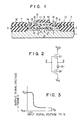
- CMOS inverter with a cross section shown in Fig. 1 has been known (c.f. document "IEEE Electron Device Letters", Volume EDL-2, No. 10, October 1981, pages 250 and 251 which discloses a similar CMOS inverter).
- a field oxide layer 2 for electrically isolating semi- conductor elements one from another is provided on one of the surface regions of a P type silicon substrate 1.
- An n" type source region 3 and an n + type drain region 4, which are electrically isolated from each other, are provided in the land substrate region isolated by the field oxide layer 2.
- a gate oxide layer 5 is provided on the surface of the substrate region located between the source and drain regions.
- a gate electrode 6 is laid over the gate oxide layer 5.
- the surfaces of the gate electrode 6, the source region 3 and the drain region 4 are covered with a CVD-SiO z layer 7.
- the Si0 2 layer 7 on the surface of the gate electrode 6 serves as a gate oxide layer of a p-channel MOS transistor to be described later.
- a through-hole 8 is formed in a part of a region of the CVD-Si0 2 layer 7, which faces the source region 3.
- a polycrystalline silicon layer 9 is provided laying over the gate electrode 6, at least a portion of the source region 3, and the drain region 4.
- a portion of the polycrystalline silicon layer 9, which is located facing the gate electrode 6, is formed as an electrical isolating layer.'A portion of the same, which faces the source region 3, is used as a p' source region 10. A portion of the same confronts a p + drain region 11. The p + source region 10 is in contact with the n + source region 3 through the through-hole 8 of the CVD-Si0 2 layer 7. The entire surface of the semiconductor device of Fig. 1 containing the polycrystalline silicon layer 9 is covered with an interlayer insulation layer 12 made of CVD-Si0 2 layer.
- An aluminium interconnection electrode 14 (power source electrode), which comes in contact with the n' drain region 4 through a contact hole 13 passing through the interlayer 12 and the CVD-SiO z layer 7, is formed on the insulation layer 12. Also formed on the insulation layer 12 is another aluminium interconnection electrode 15 (the other power source electrode) connected to the p + drain region 11 through the contact hole 13 passing through the insulation layer 12. Another aluminium connection electrode 16 (signal output electrode) is further formed on the insulation layer 12 and is connected to the p + source region 10 through a contact hole 13 passing through the insulation layer 12.
- the CMOS inverter thus structured contains an n-channel MOS transistor formed in the semiconductor substrate 1, a p-channel MOS transistor formed by the polycrystalline silicon layer 9 layered through an insulation layer over the n-channel MOS transistor, the gate electrode 6 being commonly used for the n-channel MOS transistor and the p-channel MOS transistor.
- FIG. 2 An equivalent circuit of the CMOS inverter shown in Fig. 1 is illustrated in Fig. 2.
- Q1 corresponds to the p-channel MOS transistor
- Q2 the n-channel MOS transistor
- G the gate electrode 6, 0 a signal output electrode 16, V DD a power source electrode 15, and V ss a power source electrode 14.
- the power source electrode V SS is set at an earth potential and the power source electrode V DD at 1 to 5 V, for driving the inverter.
- the signal output electrode 16 normally contacts the p + source region 10 of the polycrystalline silicon layer 9 forming the p-channel MOS transistor.
- the source region 3 of the n-channel MOS transistor directly contacts the source region 10 of the p-channel MOS transistor through the through hole 8. Therefore, a p-n junction is formed between the source regions 3 and 10.
- a parasitic diode D1 with a polarity as shown is formed between the source region 3 of the n-channel MOS transistor Q2 and the signal output terminal O.
- the parasitic diode D1 When the parasitic diode D1 is present, the output signal voltage from the output signal terminal O exhibits a response characteristic against an input signal voltage supplied to the gate terminal G, as shown in Fig.
- the output voltage from the signal output terminal 0 cannot have the level of V SS , but has a level of V, which is a potential difference at the p-n junction of the parasitic diode D1.
- the amplitude of the output signal voltage becomes smaller by V B than when the parasitic diode D1 is not present. This implies that it is very difficult to distinctively recognize the level state of the output signal voltage, that is, whether the level of the output signal voltage is "0" or "1".
- the potential difference at the p-n junction is approximately 0.7 V. Accordingly, when the power source voltage V DD is low, it is very difficult to distinguish the different level states of the output signal voltage.
- the CMOS inverter in which a p-channel MOS transistor is formed in the silicon substrate 1 and an n-channel MOS transistor is formed by the polycrystalline silicon layer 9, is also attendent with the parasitic diode.
- the p-channel MOS transistor is denoted as Q1' and the n-channnel MOS transistor as Q2'.
- the parasitic diode D2 is inserted between the signal voltage output terminal O and the source of the transistor Q1'.
- a graph is Fig. 5 represents a response characteristic of an output signal voltage against an input signal voltage level to the gate G.
- the power source voltage V DD is reduced by a potential difference V B at the p-n junction of the parasitic diode D2, and is derived from the output signal terminal O.
- an object of the present invention is to provide a stacked CMOS inverter with a structure which rejects the formation of a parasitic diode between the source region and the signal output terminal of the n-channel MOS transistor.
- a stacked CMOS inverter comprising: a semiconductor substrate of first conductivity type; an MOS transistor of second conductivity type including a first source region and a first drain region, which are of second conductivity type, provided in one of the surface regions of the semiconductor substrate and electrically isolated from each other, a first insulation layer provided on said semiconductor substrate between said first source region and said first drain region and serving as a first gate insulation layer, and a gate electrode provided on said first gate insulation layer (107), a second insulation layer for covering the surfaces of said gate electrode, said first source region and said first drain region, an MOS transistor of first conductivity type including a semiconductor layer formed on said second insulation layer which has a portion facing said gate electrode and serving as a channel region of said first conductivity type MOS transistor, a portion facing said first source region and serving as a second source region or first conductivity type, and a portion facing said first drain region and serving as a second drain region of first conductivity type, and said gate electrode, said second insulation layer interposed between said gate
- the formation of a parasitic diode between the first and second source regions is eliminated.
- This feature allows the inverter to have an output signal with a large amplitude. The level state of the output signal can be distinctively recognized. Further, if a given metal silicide layer is formed on both upper surfaces of the first source region and the first drain region, the sheet resistances of the first source region and the first drain region are reduced.
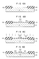
- the polycrystalline silicon layer pattern 112 is irradiated with an energy beam such as a laser beam to monocrystalline the silicon layer pattern 112 or to improve the crystallization.
- an energy beam such as a laser beam
- the resist pattern is removed.
- the semiproduct is then subjected to a heat treatment to activate the boron ion-implanted layer in ths polycrystalline silicon layer pattern 112.
- a p + type source region 114 and a p + type drain region 115 are formed.
- the p + type source region 114 of the polycrystalline silicon layer pattern 112 electrically contacts the n + type source region 105 provided in the substrate 101 through the through-hole 111 provided through the CVD-Si0 2 layer 110 and the PtSi layer 109 1 .
- a CVD-Si0 2 layer 116 with a thickness of 800 nm 8,000 A) is deposited on the entire surface, and then contact holes 117 are formed in the layer 116. Then, an aluminium layer is deposited on the entire surface of the layer 116.
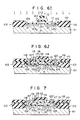
- the aluminium layer is patterned to form an AI interconnection electrode (one power source electrode) 118 connected to the PtSi layer 109 2 on the n + drain region 106 through a contact hole 117, an AI interconnection electrode (the other power source electrode) 119 connected to the p + type drain region 115 through a contact hole 117, and an interconnection electrode (signal output electrode) 120 connected through the contact hole 117 to the PtSi layer 109 1 on the n + type source region 105 (Fig. 6J).
- a diffusing rate of impurities in the PtSi layer 109, intervening between the source region 105 of the n-channel MOS transistor and the source region 114 of the p-channel MOS transistor is very small. Therefore, it is possible for boron contained in the p+ type source region 114 to diffuse into the n + type source region 105. This low rate of boron diffusion further prevents boron in the P + type source region 114 from passing through the n + type source region 105 to diffuse into the silicon substrate 101 and to short both the p + type source region 114 and the silicon substrate 101.
- the above effects are especially pronounced when the element-forming regions on the substrate 101 are made smaller, and thus the n + type source and drain regions are made shallower. Further, when the source and drain regions 105 and 106 are shallowly formed, the increase in the sheet resistance of these regions can be kept low with the metal silicide layers 109, and 109 2 . As a result, the inverter can be operated at high speed.
- the same effects can be attained in the case of a stacked CMOS inverter in which a p-channel MOS transistor is formed in the substrate and an n-channel MOS transistor is formed by a polycrystalline silicon layer pattern 112.
- the gate electrode 104 is not limited to PtSi, but may be formed of a metal such as Mo, W or Pd, or a silicide of these metals or polycrystalline silicon.
- FIG. 7 Another embodiment of the semiconductor device of the present invention shown in Fig. 7 is different from that of Fig. 6 only in that the signal output electrode 120' is made to contact the p + type source region 114 of the polycrystalline silicon layer pattern 112 through the contact hole 117'.
- the operation and effects of the embodiment of Fig. 7 are the same as those of Fig. 6J.
Landscapes
- Metal-Oxide And Bipolar Metal-Oxide Semiconductor Integrated Circuits (AREA)
- Thin Film Transistor (AREA)
- Logic Circuits (AREA)
- Electrodes Of Semiconductors (AREA)
Claims (6)
Applications Claiming Priority (2)
| Application Number | Priority Date | Filing Date | Title |
|---|---|---|---|
| JP57092923A JPS6051272B2 (ja) | 1982-05-31 | 1982-05-31 | 積層型cmosインバ−タ装置 |
| JP92923/82 | 1982-05-31 |
Publications (2)
| Publication Number | Publication Date |
|---|---|
| EP0096734A1 EP0096734A1 (de) | 1983-12-28 |
| EP0096734B1 true EP0096734B1 (de) | 1986-08-20 |
Family
ID=14068001
Family Applications (1)
| Application Number | Title | Priority Date | Filing Date |
|---|---|---|---|
| EP83103407A Expired EP0096734B1 (de) | 1982-05-31 | 1983-04-07 | Inverter mit übereinanderliegendem komplementären Metall-Oxyd-Halbleiter |
Country Status (4)
| Country | Link |
|---|---|
| US (1) | US4698659A (de) |
| EP (1) | EP0096734B1 (de) |
| JP (1) | JPS6051272B2 (de) |
| DE (1) | DE3365398D1 (de) |
Families Citing this family (25)
| Publication number | Priority date | Publication date | Assignee | Title |
|---|---|---|---|---|
| US4521952A (en) * | 1982-12-02 | 1985-06-11 | International Business Machines Corporation | Method of making integrated circuits using metal silicide contacts |
| JPS60130160A (ja) * | 1983-12-19 | 1985-07-11 | Hitachi Ltd | 半導体記憶装置 |
| JPS60140873A (ja) * | 1983-12-28 | 1985-07-25 | Fujitsu Ltd | 半導体装置 |
| JPS6164166A (ja) * | 1984-09-06 | 1986-04-02 | Toshiba Corp | 半導体装置 |
| US4811078A (en) * | 1985-05-01 | 1989-03-07 | Texas Instruments Incorporated | Integrated circuit device and process with tin capacitors |
| JPS6312168A (ja) * | 1986-07-03 | 1988-01-19 | Oki Electric Ind Co Ltd | Lddmis型電界効果トランジスタ |
| JPS6381948A (ja) * | 1986-09-26 | 1988-04-12 | Toshiba Corp | 多層配線半導体装置 |
| US5166770A (en) * | 1987-04-15 | 1992-11-24 | Texas Instruments Incorporated | Silicided structures having openings therein |
| JPH0714009B2 (ja) * | 1987-10-15 | 1995-02-15 | 日本電気株式会社 | Mos型半導体記憶回路装置 |
| US4994873A (en) * | 1988-10-17 | 1991-02-19 | Motorola, Inc. | Local interconnect for stacked polysilicon device |
| US5306935A (en) * | 1988-12-21 | 1994-04-26 | Texas Instruments Incorporated | Method of forming a nonvolatile stacked memory |
| US5066613A (en) * | 1989-07-13 | 1991-11-19 | The United States Of America As Represented By The Secretary Of The Navy | Process for making semiconductor-on-insulator device interconnects |
| US5452247A (en) * | 1989-12-20 | 1995-09-19 | Fujitsu Limited | Three-dimensional static random access memory device for avoiding disconnection among transistors of each memory cell |
| JP2996694B2 (ja) * | 1990-06-13 | 2000-01-11 | 沖電気工業株式会社 | 半導体スタックトcmos装置の製造方法 |
| DE69128876T2 (de) * | 1990-11-30 | 1998-08-06 | Sharp Kk | Dünnfilm-Halbleitervorrichtung |
| US5684320A (en) * | 1991-01-09 | 1997-11-04 | Fujitsu Limited | Semiconductor device having transistor pair |
| US5057888A (en) * | 1991-01-28 | 1991-10-15 | Micron Technology, Inc. | Double DRAM cell |
| US5154514A (en) * | 1991-08-29 | 1992-10-13 | International Business Machines Corporation | On-chip temperature sensor utilizing a Schottky barrier diode structure |
| US5330929A (en) * | 1992-10-05 | 1994-07-19 | Motorola, Inc. | Method of making a six transistor static random access memory cell |
| JPH06140519A (ja) * | 1992-10-22 | 1994-05-20 | Toshiba Corp | 半導体装置及びその製造方法 |
| US5872029A (en) * | 1996-11-07 | 1999-02-16 | Advanced Micro Devices, Inc. | Method for forming an ultra high density inverter using a stacked transistor arrangement |
| US5926700A (en) | 1997-05-02 | 1999-07-20 | Advanced Micro Devices, Inc. | Semiconductor fabrication having multi-level transistors and high density interconnect therebetween |
| US5888872A (en) | 1997-06-20 | 1999-03-30 | Advanced Micro Devices, Inc. | Method for forming source drain junction areas self-aligned between a sidewall spacer and an etched lateral sidewall |
| US5818069A (en) * | 1997-06-20 | 1998-10-06 | Advanced Micro Devices, Inc. | Ultra high density series-connected transistors formed on separate elevational levels |
| CN102487085B (zh) * | 2010-12-01 | 2014-04-23 | 中国科学院微电子研究所 | 半导体器件及其制造方法 |
Citations (1)
| Publication number | Priority date | Publication date | Assignee | Title |
|---|---|---|---|---|
| EP0017697A1 (de) * | 1979-03-01 | 1980-10-29 | International Business Machines Corporation | Verbindungsvorrichtung für integrierte Halbleiterschaltungen und Verfahren zu ihrer Herstellung |
Family Cites Families (8)
| Publication number | Priority date | Publication date | Assignee | Title |
|---|---|---|---|---|
| NL190710C (nl) * | 1978-02-10 | 1994-07-01 | Nec Corp | Geintegreerde halfgeleiderketen. |
| IT1110843B (it) * | 1978-02-27 | 1986-01-06 | Rca Corp | Contatto affondato per dispositivi mos di tipo complementare |
| US4333099A (en) * | 1978-02-27 | 1982-06-01 | Rca Corporation | Use of silicide to bridge unwanted polycrystalline silicon P-N junction |
| US4343082A (en) * | 1980-04-17 | 1982-08-10 | Bell Telephone Laboratories, Incorporated | Method of making contact electrodes to silicon gate, and source and drain regions, of a semiconductor device |
| JPS5846193B2 (ja) * | 1980-07-15 | 1983-10-14 | 株式会社東芝 | 半導体装置 |
| JPS5743455A (en) * | 1980-08-29 | 1982-03-11 | Fujitsu Ltd | Complementary type semiconductor device |
| US4374700A (en) * | 1981-05-29 | 1983-02-22 | Texas Instruments Incorporated | Method of manufacturing silicide contacts for CMOS devices |
| JPS57204171A (en) * | 1981-06-10 | 1982-12-14 | Mitsubishi Electric Corp | Semiconductor device |
-
1982
- 1982-05-31 JP JP57092923A patent/JPS6051272B2/ja not_active Expired
-
1983
- 1983-04-07 EP EP83103407A patent/EP0096734B1/de not_active Expired
- 1983-04-07 DE DE8383103407T patent/DE3365398D1/de not_active Expired
-
1986
- 1986-05-16 US US06/865,652 patent/US4698659A/en not_active Expired - Lifetime
Patent Citations (1)
| Publication number | Priority date | Publication date | Assignee | Title |
|---|---|---|---|---|
| EP0017697A1 (de) * | 1979-03-01 | 1980-10-29 | International Business Machines Corporation | Verbindungsvorrichtung für integrierte Halbleiterschaltungen und Verfahren zu ihrer Herstellung |
Non-Patent Citations (2)
| Title |
|---|
| IEEE Electron Devices Letters, Vol. ED.EDL-1 (1980, 06), pages 117-118 * |
| IEEE Journal of Solid-State Circuits, Vol. SC-17(1982,04), pages 215-219 * |
Also Published As
| Publication number | Publication date |
|---|---|
| EP0096734A1 (de) | 1983-12-28 |
| JPS58210656A (ja) | 1983-12-07 |
| US4698659A (en) | 1987-10-06 |
| DE3365398D1 (en) | 1986-09-25 |
| JPS6051272B2 (ja) | 1985-11-13 |
Similar Documents
| Publication | Publication Date | Title |
|---|---|---|
| US4698659A (en) | Stacked complementary metal oxide semiconductor inverter | |
| EP0341821B1 (de) | Verfahren zur Herstellung einer Halbleitervorrichtung | |
| US5294822A (en) | Polycide local interconnect method and structure | |
| US4845532A (en) | Semiconductor devices | |
| JPS60226163A (ja) | シヨツトキ−バイポ−ラトランジスタを有するcmos構造を製造する方法 | |
| US4396930A (en) | Compact MOSFET device with reduced plurality of wire contacts | |
| JPS6379368A (ja) | ポリシリコンエミッタ及びシリサイド化ベ−スを持った高性能BiCMOS構成体の製造方法 | |
| US4965216A (en) | Method of fabricating a bi-CMOS device | |
| JP2687890B2 (ja) | Mos型半導体装置の製造方法 | |
| EP0337481B1 (de) | Halbleitervorrichtung | |
| JPH05275546A (ja) | 半導体デバイス及びその新規な埋込み相互接続構造並びにそれぞれを形成する方法 | |
| US5057894A (en) | Semiconductor integrated circuit device | |
| JP2549726B2 (ja) | 半導体集積回路とその製造方法 | |
| WO1983001538A1 (en) | High density cmos devices with conductively interconnected wells and method of fabricating the same | |
| US5612243A (en) | Polycide local interconnect method and structure | |
| JP2753301B2 (ja) | 半導体集積回路装置 | |
| US5336911A (en) | Semiconductor device | |
| JPS6380560A (ja) | 最小数のマスクを使用してバイポ−ラ及び相補型電界効果トランジスタを同時的に製造する方法 | |
| JPS6334619B2 (de) | ||
| US5254874A (en) | High density local interconnect in a semiconductor circuit using metal silicide | |
| JPH10284438A (ja) | 半導体集積回路及びその製造方法 | |
| JPH0644631B2 (ja) | 半導体装置及びその製造方法 | |
| WO1997049131A1 (en) | Semiconductor device with buried conductive silicide layer | |
| JPH02237024A (ja) | 半導体装置及びその製造方法 | |
| JPH03152939A (ja) | 半導体集積回路装置 |
Legal Events
| Date | Code | Title | Description |
|---|---|---|---|
| PUAI | Public reference made under article 153(3) epc to a published international application that has entered the european phase |
Free format text: ORIGINAL CODE: 0009012 |
|
| 17P | Request for examination filed |
Effective date: 19830504 |
|
| AK | Designated contracting states |
Designated state(s): DE FR GB |
|
| RAP1 | Party data changed (applicant data changed or rights of an application transferred) |
Owner name: KABUSHIKI KAISHA TOSHIBA |
|
| GRAA | (expected) grant |
Free format text: ORIGINAL CODE: 0009210 |
|
| AK | Designated contracting states |
Kind code of ref document: B1 Designated state(s): DE FR GB |
|
| ET | Fr: translation filed | ||
| REF | Corresponds to: |
Ref document number: 3365398 Country of ref document: DE Date of ref document: 19860925 |
|
| PLBE | No opposition filed within time limit |
Free format text: ORIGINAL CODE: 0009261 |
|
| STAA | Information on the status of an ep patent application or granted ep patent |
Free format text: STATUS: NO OPPOSITION FILED WITHIN TIME LIMIT |
|
| 26N | No opposition filed | ||
| PGFP | Annual fee paid to national office [announced via postgrant information from national office to epo] |
Ref country code: GB Payment date: 19970401 Year of fee payment: 15 |
|
| PGFP | Annual fee paid to national office [announced via postgrant information from national office to epo] |
Ref country code: FR Payment date: 19970409 Year of fee payment: 15 |
|
| PGFP | Annual fee paid to national office [announced via postgrant information from national office to epo] |
Ref country code: DE Payment date: 19970414 Year of fee payment: 15 |
|
| PG25 | Lapsed in a contracting state [announced via postgrant information from national office to epo] |
Ref country code: GB Free format text: LAPSE BECAUSE OF NON-PAYMENT OF DUE FEES Effective date: 19980407 |
|
| PG25 | Lapsed in a contracting state [announced via postgrant information from national office to epo] |
Ref country code: FR Free format text: THE PATENT HAS BEEN ANNULLED BY A DECISION OF A NATIONAL AUTHORITY Effective date: 19980430 |
|
| GBPC | Gb: european patent ceased through non-payment of renewal fee |
Effective date: 19980407 |
|
| PG25 | Lapsed in a contracting state [announced via postgrant information from national office to epo] |
Ref country code: DE Free format text: LAPSE BECAUSE OF NON-PAYMENT OF DUE FEES Effective date: 19990202 |
|
| REG | Reference to a national code |
Ref country code: FR Ref legal event code: ST |