EP0098417A2 - Halbleiterspeicheranordnung - Google Patents
Halbleiterspeicheranordnung Download PDFInfo
- Publication number
- EP0098417A2 EP0098417A2 EP83105819A EP83105819A EP0098417A2 EP 0098417 A2 EP0098417 A2 EP 0098417A2 EP 83105819 A EP83105819 A EP 83105819A EP 83105819 A EP83105819 A EP 83105819A EP 0098417 A2 EP0098417 A2 EP 0098417A2
- Authority
- EP
- European Patent Office
- Prior art keywords
- mos transistor
- resistor
- node
- memory device
- semiconductor memory
- Prior art date
- Legal status (The legal status is an assumption and is not a legal conclusion. Google has not performed a legal analysis and makes no representation as to the accuracy of the status listed.)
- Ceased
Links
Images


Classifications
-
- G—PHYSICS
- G11—INFORMATION STORAGE
- G11C—STATIC STORES
- G11C11/00—Digital stores characterised by the use of particular electric or magnetic storage elements; Storage elements therefor
- G11C11/21—Digital stores characterised by the use of particular electric or magnetic storage elements; Storage elements therefor using electric elements
- G11C11/34—Digital stores characterised by the use of particular electric or magnetic storage elements; Storage elements therefor using electric elements using semiconductor devices
- G11C11/40—Digital stores characterised by the use of particular electric or magnetic storage elements; Storage elements therefor using electric elements using semiconductor devices using transistors
- G11C11/41—Digital stores characterised by the use of particular electric or magnetic storage elements; Storage elements therefor using electric elements using semiconductor devices using transistors forming static cells with positive feedback, i.e. cells not needing refreshing or charge regeneration, e.g. bistable multivibrator or Schmitt trigger
- G11C11/412—Digital stores characterised by the use of particular electric or magnetic storage elements; Storage elements therefor using electric elements using semiconductor devices using transistors forming static cells with positive feedback, i.e. cells not needing refreshing or charge regeneration, e.g. bistable multivibrator or Schmitt trigger using field-effect transistors only
- G11C11/4125—Cells incorporating circuit means for protecting against loss of information
Definitions
- the present invention relates to a semiconductor memory device having improved reliability which can prevent the occurrence of a soft error due to the incidence of alpha particles.
- each memory cell is composed of a single capacitor and a single MOS (metal oxide semiconductor) transistor.
- MOS metal oxide semiconductor
- each memory cell is composed of four transistors 11 to 14 and two load resistors 15 and 16.
- characters BL and BL indicate a pair of bit lines and WL a word line.
- the static type semiconductor memory device is constructed so as to hold data by always feeding current through a resistor (15 or 16 in Fig. 1). Because of this feature, in the static type semiconductor memory device, the cccurrence of a soft error is less frequent than in the dynamic type semiconductor memory device. Nevertheless, miniaturization and low power dissipation of the elements of the semiconductor memory device increases the probability that a soft error will occur. More specifically, in a static type semiconductor memory device as shown in Fig. 1, as the degree of miniaturization increases, stray capacitances at the nodes Nl and N2 of load resistors 15 and 16 and drive transistors 11 and 12 become smaller.
- the integration density of a semiconductor chip reflecting the present stage of semiconductor technology allows the stray capacitance at the node N2 to be approximately 10 fF (10x10-15 F) and hence, a quantity of charges allowed to be stored at the node N2 is 50 fC (50x10-15 C) at the most.
- a current I a flows along a path between the node N2 and ground.
- the current I a is a pulsative current with a very narrow width, its peak value is 300 - 400 pA, and the total quantity of its charge reaches 100 fC.
- the total quantity of the charge of the current I a is remarkably larger than the quantity of charge stored in the node N2. Therefore, the flow of the current into the node N2 results in destruction of the data stored therein. Further, the decreased power dissipation necessitates an extreme increase in resistance of the resistors 15 and 16 (up to the order of giga-ohms). The result is that the current flowing from the power source V CC into the node N2 becomes small, and hence, the quantity of charge stored in the node N2 also becomes small. This implies that the stored data is more easily destroyed by alpha particles.
- an object of the present invention is to provide a semiconductor memory device which can prevent stored data from being destroyed by the incident alpha particles and hence, improve the reliability of the device.
- a semiconductor memory device comprising:
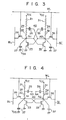
- Fig. 3 shows an embodiment of a semiconductor memory device according to the present invention.
- a first series circuit comprises a pair of resistors 21 and 22 and a MOS transistor 23 connected between the power source voltage V CC and the reference voltage V SS or ground.
- the resistors 21 and 22 and the MOS transistor 23 are connected in this order between the power source voltage V CC and the reference voltage V SS .
- the resistors 21 and 22 and the MOS transistor 23 cooperate to form a first inverter 24 in which the resistors 21 and 22 are used as a load and the MOS transistor 23 as a driver.
- a junction point of the resistor 22 and the MOS transistor 23 is used as an output electrode node Nl.
- a second series circuit comprised of resistors 31 and 32 and a MOS transistor 33, is inserted between the power source voltage V CC and the reference voltage V SS .
- the resistors 31 and 32 and the MOS transistor 33 are connected, in this order, to the power source voltage V CC .
- These resistors 31 and 32 and the MOS transistor 33 form a second inverter 34, in which the resistors 31 and 32 serve as a load and the MOS transistor 33 as a driver.
- a junction point between the resistor 32 and the MOS transistor 33 is used as an output electrode node N2 of the second inverter 34.
- the output node Nl of the inverter 24 is connected to the gate of the transistor 33 as an input node of the second inverter 34.
- the output node N2 of the inverter 34 is connected to the gate of the transistor 23 as an input node of the inverter 24.
- the two inverters 24 and 34 are crossed such that the input node of one of the inverters is connected to the output node of the other, thereby forming a flip-flop 40 for storing one- bit data.
- An interconnection point between the resistors 21 and 22 is connected to one end of a capacitor 25 whose output is connected to an output node N2 of the inverter 34.
- an interconnection point between the resistors 31 and 32 is connected to one end of a capacitor 35 whose other end is connected to an output node N1 of the inverter 24.
- a MOS transistor 26 is connected between the output node N1 of the inverter 24 and a bit line BL.
- a MOS transistor 36 for data transfer is provided between an output node N2 of the inverter 34 and the other bit line BL.
- the gates of the MOS transistors 26 and 36 are connected together and to the word line WL.
- a capacitance 27 exists between the output node N1 of the inverter 24 and the reference voltage V SS .
- the capacitance 27 generally represents various types of capacitances present at the node Nl, such as the junction capacitances between the sources of the transistors 23 and 26 and the substrate and between the drains thereof and the substrate, and gate capacitances of the transistors 23 and 26.
- a capacitance 37 exists between the output node of the inverter 34 and ground, and is generally representative of various types of capacitances existing therebetween, such as junction capacitances between the sources of the transistors 33 and 36 and the substrate, and between the drains of these transistors and the substrate, and the gate capacitances of these transistors.
- the MOS transistors are all of the enhancement, n-channel type.
- resistances of the resistors 21 and 22 and the resistors 31 and 32 are set at Rl to R4, and the capacitances of the capacitors 25 and 35 at Cl and C3, respectively.
- the capacitances of the capacitors 27 and 37 are set at C2 and C4, respectively.
- V TN may vary according to various factors pertaining to the transistors 23 and 33, e.g. channel width, impurity concentration, etc. However, V TN is generally about half the threshold voltage.
- a low logic level (“L” level) and a high logic level (“H” level) are applied to the bit lines BL and BL, respectively.
- a write mode designating signal (R/W) at "H” level is input to the word line WL to set up a data write mode.
- R/W write mode designating signal
- both the MOS transistors 26 and 36 are turned on.
- the "H” and “L” level signals on the bit lines BL and BL, respectively render the nodes N1 and N2 "L” and “H” level, respectively.
- the R/W signal is set at "L” level, so that the MOS transistors 26 and 36 are both turned off.
- the write operation is completed.
- the data of "L” level has been written into the node N1 and the data of "H” level has been written into the node N2. That is, the flip-flop 40 is set to "0" level at the node Nl and "1" level at the node N2.
- the capacitor 37 is charged with a higher potential at the portion thereof which is closer to the node N2.
- the quantity of charge stored in the capacitor becomes smaller with the increase in the integration density of the IC chip.
- the charge quantity caused by the incidence of alpha particles depends very little on the improvement of the integration density, i.e., the miniaturization of the elements. In other words, it should not be expected that it will be decreased by miniaturizing the elements. With the further miniaturization of the elements in the future, the charges stored in the capacitor 37 will be almost fully discharged within the period of the pulse width t d of the current I a arising from the incidence of the alpha particles.
- the resistances Rl and R3 of the resistors 21 and 31 are set on the order of giga-ohms to provide for power-saving of the device. Therefore, the quantity of the charge from the power source voltage V CC to the node N2 through the resistors 21 and 31 is almost negligible.
- the potential on a node N2 after an interval several times the pulse width t d of the current I a is substantially determined only by a redistribution of charges by three capacitors 25, 35 and 37.
- the flip-flop 40 returns to the original state.
- the reason for this is as follows.
- the transistor 23 When the transistor 23 is turned on, the nodes Nl and N2 are charged through the resistors 21, 22 and 31, 32, respectively, by the power source V CC .
- the potential of the node N2 is higher by V TN than that of the node Nl, the node N2 is charged to the threshold voltage of the transistor 23 before the node Nl is charged to the threshold voltage of the transistor 23.
- the transistor 23 is turned on, and thus the flip-flop 40 returns to the original, state.
- "high" level data on the node N2 is preserved since it is not destroyed through the discharge following the incidence of alpha particles.
- the incidence of the alpha particles does not lead to destruction of data or generation of an error.
- the potential V TN on the node N2 which has stored high level data after the charge redistribution is set higher than the potential on the output node Nl of the transistor 23. With this potential setting, even when the current I a flows into the node N2 due to the incidence of the current I ⁇ , the data stored in node N2 is protected. Further, note that inequalities (11) and (13) are equal to (4) and (2).
- the potential of the node Nl after the charge redistribution is higher than the minimum potential difference V TN , the "high" level data on the node Nl is kept as it is, through the process such as at the node N2.
- the potential on the node Nl after the charge redistribution must be higher than the minimum potential difference V TN , v i z . the following relation must be satisfied
- Relations (3) and (4) are for determining a minimum value of C1R2 or C3R4. If the values of ClR2 and C3R4 are set to excessively large values, a situation may occur wherein data cannot be written within a write period in a write mode. Therefore, to prevent the occurrence of such a situation, it is necessary to satisfy inequalities (5) and (6) in order to determine the maximum values of C1R2 and C3R4.
- the resistors 22 and 32 may be formed by a distributed constant circuit containing the electrodes of the capacitors 25 and 35.
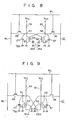
- Fig. 4 shows a circuit diagram of another embodiment of the present invention.
- first ends of the capacitors 25 and 35 are connected to nodes N3 and N4 connected to the power source voltage V CC and reference voltage V SS , not the nodes N2 and Nl.
- nodes N3 and N4 may be connected to the voltages with opposite polarities or together to the reference voltage V SS or the power source voltage V CC .
- Rl>R2 and R3> R 4 parameters are selected which satisfy the _following relations (16) - (21).
- the potential on the node N1 or N2 after the charge redistribution is set higher than the minimum potential difference V TN . If the current I a flows into the node Nl or N2, the "high" level data stored in the node Nl or N2 is not destroyed.
- the relations (22) and (23), and (24) and (25) are equal to (19) and (17), and (18) and (16), respectively.
- the inequalities (22) and (24) are used to determine minimum values of the C1R2 and C3R4. As in the previous embodiments, if the C1R2 and C3R4 are too large, it becomes impossible to write data within the write period. To avoid such a situation, the maximum values of C1R2 and C3R4 are first selected and then C1R2 and C3R4 must be set below these maximum values. In other words, C1R2 and C3R4 must be selected so as to satisfy the inequalities (20) and (21).
- Fig. 5 shows a circuit diagram of still another embodiment of the present invention.
- the first ends of the two capacitors in the Fig. 3 or Fig. 4 embodiment are interconnected to form a single capacitor 45.
- the capacitance of the capacitor 45 is C5 and Rl> R 2 and R3> R4 . Under this condition, the circuit is designed to satisfy the relations (26) - (30).
- the charge redistribution after negative charges have flowed into the nodes Nl and N2 as the result of the incidence of alpha particles is set up by the current flowing through the two resistors 22 and 32 which is caused by the discharge from the capacitor 45.
- solving the inequality expressing a relationship of the potentials on the nodes Nl and N2 after the charge redistribution to the minimum potential difference V TN we have relations equal to the relations (26) - (28).
- the relations giving the maximum values of the C5R2 and C5R4 are equal to the relations (29) - (30).
- each factor when the resistances of the load resistors 21, 22, 31 and 32 for the pair of inverters 24 and 34 are Rl to R4, these are related as follows: Rl> R 2 and R3>R4. Conversely, these relations of the resistances may be Rl ⁇ R2 and R3 ⁇ R4. To apply the latter relation to the Fig. 3 embodiment, each factor must be selected so as to satisfy the following inequalities (31) - (36), not. (1) - (6).
- FIG. 6 there is shown yet another embodiment of the present invention.
- This embodiment is not provided with capacitors 25 and 35 as are used in the Fig. 3 embodiment.
- Reference numerals 25A and 35A denote capacitors existing between the gate electrode nodes of the transistors 23 and 33 and ground.
- the gate of the MOS transistor 23 is connected to a junction between the resistors 31 and 32.
- the gate of the MOS transistor 33 is connected to the junction between the resistors 21 and 22.
- the capacitances of the capacitors 25A and 35A are Cl and C3, and Rl>R2 and R3> R 4
- the Fig. 6 circuit must be designed so as to satisfy the following relations (37) - (42).
- the potential on the node N2 is determined by the charge redistribution of the residual charge in the capacitors 35 and 37.
- the potential on the node N2 after the charge redistribution is given by V oC3 e- t d/ C3R 4/( C3 +C4).
- the circuit designed so as to satisfy inequalities (46) and (47) can prevent the data from being destroyed.
- the relations (39) and (40) are used to determine the minimum values of the C1R2 and C3R4. If the ClR2 and C3R4 are made excessively large, the data may not be able to be written in the write mode within the write period. Accordingly, to prevent this state, it is necessary to satisfy inequalities (41) and (42) for determining the maximum values of these factors.
- the resistors 22 and 32 may be formed by a distributed constant circuit containing the electrodes of the capacitors 25 and 35.
- the output nodes N1 and N2 of the MOS transistors 23 and 33 are respectively connected through parts of the load resistors, i.e., the load resistor 22 of the resistors 21 and 22 and the load resistor 32 of the resistors 31 and 32, to - the gates of the MOS transistors 33 and 23.
- Fig. 7 shows a further embodiment of the present invention, in which additional resistors are used instead of the load resistors in the Fig. 6 embodiment. Further, the output node of the MOS transistor is connected to the gate of the MOS transistor.
- a resistor 41 connected between the output node N1 of the MOS transistor 23 and the power source voltage V CC is used for the load resistor of the MOS transistor 23. That is, a resistor 42 is formed in an interconnection wiring connecting the output node N1 and the gate of the MOS transistor 33, that is, in a portion of .a wiring connecting the output node N1 to the gate of the MOS transistor 33, but excluding the electrode portion of the output node N1 and the gate electrode portion of the MOS transistor 33.
- a resistor 43 connected between the output node N2 of the MOS transistor 33 and the power source voltage V CC is used for the load resistor of the MOS transistor 33.
- a resistor 44 is formed in an interconnection wiring connecting the output node N2 to the gate of the MOS transistor 23, viz. a portion of a wiring connecting the output node N2 and the gate of the MOS transistor 23, but excluding the electrode portion of the output node N2 and the gate electrode portion of the MOS transistor 23.
- the resistances of resistors 41 to 44 are set at Rl to R4 as in each of the above-mentioned embodiments.
- the data can be prevented from being destroyed.
- a junction of the output node Nl of the MOS transistor 23 and the gate of the MOS transistor 33 is connected to a junction of the output node N2 of the MOS transistor 33 and the gate of the transistor 23 through a resistor formed in a portion of a wiring connecting them, but excluding the electrode portions therein.
- the resistor can be formed in the gate electrode portion of each of the transistors 23 and 33 in the interconnection wiring, and, through this resistor, the node Nl of the transistor 23 and the gate of the transistor 33 can be connected to the node N2 of the transistor 33 and the gate of the transistor 23.
- FIG. 8 An embodiment implementing such an idea is shown in Fig. 8.
- the output node Nl of the transistor 23 is connected to the power source voltage V CC through the resistor-51, and is connected to the gate of the MOS transistor 33 through a resistor 52 formed in the gate electrode portion in the interconnection wiring connecting the node N1 and the gate of the MOS transistor 33.
- the output node N2 of the transistor 33 is connected through a resistor 53 as a load element to the power source voltage V CC , and is connected to . the gate of the MOS transistor 23 through the gate electrode portion in the wiring connecting the node N2 and the gate of the MOS transistor 23.
- the remaining arrangement of this embodiment is the same as that of the Fig. 6 embodiment. No further explanation thereof will be given, and like reference numerals will be used for like portions in Fig. 6.
- the resistances of the resistors 51 to 54 are set at Rl to R4, as in the above-mentioned embodiments.
- the circuit is arranged so as to satisfy relations (44) to (47), thereby preventing the occurrence of a soft error.
- the resistor 52 formed at the gate electrode node of the MOS transistor 33, together with the capacitor 25, forms a distributed constant circuit
- the resistor 54 formed at the gate electrode of the MOS transistor 23 forms a distributed constant circuit in cooperation with the capacitor 35.
- the output node N1 of the MOS transistor 23 is connected to the power source voltage V CC through a resistor 62 formed in the gate electrode portion in the wiring connecting the node N1 and the gate of the MOS transistor 33, and through a resistor 61 as a load element.
- the output node N2 of the MOS transistor 33 is connected to the power source voltage V CC through a resistor 64 formed in.the gate electrode portion in the wiring connecting the node N2 and the gate of the transistor 23, and through a load resistor 63.
- the resistance values of the resistors 61 to 64 are set at Rl to R4, respectively, and the circuit is designed so as to satisfy inequalities (44) to (47), as in the above-mentioned embodiments.
Landscapes
- Engineering & Computer Science (AREA)
- Microelectronics & Electronic Packaging (AREA)
- Computer Hardware Design (AREA)
- Static Random-Access Memory (AREA)
- Semiconductor Memories (AREA)
- Dram (AREA)
Applications Claiming Priority (4)
| Application Number | Priority Date | Filing Date | Title |
|---|---|---|---|
| JP102835/82 | 1982-06-15 | ||
| JP57102835A JPS58220297A (ja) | 1982-06-15 | 1982-06-15 | 半導体記憶装置 |
| JP39551/83 | 1983-03-10 | ||
| JP58039551A JPS59165295A (ja) | 1983-03-10 | 1983-03-10 | 半導体記憶装置 |
Related Child Applications (2)
| Application Number | Title | Priority Date | Filing Date |
|---|---|---|---|
| EP89101197.5 Division-Into | 1983-06-14 | ||
| EP89101197A Division EP0316307A1 (de) | 1982-06-15 | 1983-06-14 | Halbleiterspeicheranordnung |
Publications (2)
| Publication Number | Publication Date |
|---|---|
| EP0098417A2 true EP0098417A2 (de) | 1984-01-18 |
| EP0098417A3 EP0098417A3 (de) | 1986-12-30 |
Family
ID=26378960
Family Applications (1)
| Application Number | Title | Priority Date | Filing Date |
|---|---|---|---|
| EP83105819A Ceased EP0098417A3 (de) | 1982-06-15 | 1983-06-14 | Halbleiterspeicheranordnung |
Country Status (2)
| Country | Link |
|---|---|
| US (1) | US4532609A (de) |
| EP (1) | EP0098417A3 (de) |
Cited By (1)
| Publication number | Priority date | Publication date | Assignee | Title |
|---|---|---|---|---|
| EP0342466A3 (de) * | 1988-05-16 | 1990-11-28 | National Semiconductor Corporation | Statischer RAM-Speicher mit Immunität gegen Einzelereignisse |
Families Citing this family (22)
| Publication number | Priority date | Publication date | Assignee | Title |
|---|---|---|---|---|
| JPH0685431B2 (ja) * | 1985-06-10 | 1994-10-26 | 株式会社日立製作所 | 半導体装置 |
| JPS62273694A (ja) * | 1986-05-22 | 1987-11-27 | Sony Corp | センスアンプ |
| US4797804A (en) * | 1987-03-09 | 1989-01-10 | International Business Machines Corporation | High density, high performance, single event upset immune data storage cell |
| US5434811A (en) * | 1987-11-19 | 1995-07-18 | National Semiconductor Corporation | Non-destructive read ferroelectric based memory circuit |
| US4852060A (en) * | 1988-03-31 | 1989-07-25 | International Business Machines Corporation | Soft error resistant data storage cells |
| JPH01307095A (ja) * | 1988-06-01 | 1989-12-12 | Mitsubishi Electric Corp | 不揮発性cam |
| JP3359354B2 (ja) * | 1991-06-24 | 2002-12-24 | テキサス インスツルメンツ インコーポレイテツド | 向上されたダイナミック負フィードバッグを備えた電子ラッチ |
| US5303190A (en) * | 1992-10-27 | 1994-04-12 | Motorola, Inc. | Static random access memory resistant to soft error |
| KR100305123B1 (ko) * | 1992-12-11 | 2001-11-22 | 비센트 비.인그라시아, 알크 엠 아헨 | 정적랜덤액세스메모리셀및이를포함하는반도체장치 |
| US5377139A (en) * | 1992-12-11 | 1994-12-27 | Motorola, Inc. | Process forming an integrated circuit |
| JP2885607B2 (ja) * | 1993-05-17 | 1999-04-26 | 日本電気アイシーマイコンシステム株式会社 | 半導体メモリ |
| US5452246A (en) * | 1993-06-02 | 1995-09-19 | Fujitsu Limited | Static semiconductor memory device adapted for stabilization of low-voltage operation and reduction in cell size |
| US5572460A (en) * | 1993-10-26 | 1996-11-05 | Integrated Device Technology, Inc. | Static random-access memory cell with capacitive coupling to reduce sensitivity to radiation |
| JP3514500B2 (ja) | 1994-01-28 | 2004-03-31 | 株式会社ルネサステクノロジ | 半導体装置及びその製造方法 |
| US5861652A (en) * | 1996-03-28 | 1999-01-19 | Symbios, Inc. | Method and apparatus for protecting functions imbedded within an integrated circuit from reverse engineering |
| US5700707A (en) * | 1996-06-13 | 1997-12-23 | Chartered Semiconductor Manufacturing Pte Ltd. | Method of manufacturing SRAM cell structure having a tunnel oxide capacitor |
| US5764563A (en) * | 1996-09-30 | 1998-06-09 | Vlsi Technology, Inc. | Thin film load structure |
| US6088259A (en) * | 1999-02-19 | 2000-07-11 | Worldwide Semiconductor Manufacturing Corporation | SRAM cell using two single transistor inverters |
| JP2003173681A (ja) * | 2001-12-07 | 2003-06-20 | Mitsubishi Electric Corp | 半導体メモリ回路およびラッチ回路 |
| US7233518B2 (en) * | 2005-02-04 | 2007-06-19 | Honeywell International Inc. | Radiation-hardened SRAM cell with write error protection |
| US7876602B2 (en) * | 2007-06-18 | 2011-01-25 | Bae Systems Information And Electronic Systems Integration Inc. | Single-event upset immune static random access memory cell circuit, system, and method |
| CN112671392A (zh) * | 2020-12-24 | 2021-04-16 | 中国人民解放军国防科技大学 | 一种用于高电平复位电路的抗单粒子瞬态缓冲器 |
Family Cites Families (7)
| Publication number | Priority date | Publication date | Assignee | Title |
|---|---|---|---|---|
| US3560764A (en) * | 1967-05-25 | 1971-02-02 | Ibm | Pulse-powered data storage cell |
| US3540010A (en) * | 1968-08-27 | 1970-11-10 | Bell Telephone Labor Inc | Diode-coupled semiconductive memory |
| US4130892A (en) * | 1977-01-03 | 1978-12-19 | Rockwell International Corporation | Radiation hard memory cell and array thereof |
| US4158239A (en) * | 1977-12-20 | 1979-06-12 | International Business Machines Corporation | Resistive gate FET flip-flop storage cell |
| JPS5588356A (en) * | 1978-12-27 | 1980-07-04 | Hitachi Ltd | Semiconductor device |
| JPS564263A (en) * | 1979-06-25 | 1981-01-17 | Hitachi Ltd | Semiconductor memory |
| EP0033159B1 (de) * | 1980-01-29 | 1984-05-02 | Nec Corporation | Halbleitervorrichtung |
-
1983
- 1983-06-14 US US06/504,125 patent/US4532609A/en not_active Expired - Lifetime
- 1983-06-14 EP EP83105819A patent/EP0098417A3/de not_active Ceased
Cited By (1)
| Publication number | Priority date | Publication date | Assignee | Title |
|---|---|---|---|---|
| EP0342466A3 (de) * | 1988-05-16 | 1990-11-28 | National Semiconductor Corporation | Statischer RAM-Speicher mit Immunität gegen Einzelereignisse |
Also Published As
| Publication number | Publication date |
|---|---|
| US4532609A (en) | 1985-07-30 |
| EP0098417A3 (de) | 1986-12-30 |
Similar Documents
| Publication | Publication Date | Title |
|---|---|---|
| EP0098417A2 (de) | Halbleiterspeicheranordnung | |
| KR100285184B1 (ko) | 승압 회로 및 반도체 기억 장치 | |
| US4725981A (en) | Random access memory cell resistant to inadvertant change of state due to charged particles | |
| EP0250060B1 (de) | Nichtflüchtige Halbleiter-Speichereinrichtung | |
| EP0217601A2 (de) | Speicherzelle | |
| US4563754A (en) | Static-type random-access memory device | |
| US6373315B2 (en) | Signal potential conversion circuit | |
| KR910007436B1 (ko) | 반도체 비휘발성 메모리 장치 | |
| US4536859A (en) | Cross-coupled inverters static random access memory | |
| EP0862181A2 (de) | Statische Halbleiterspeicheranordnung mit Zeitgeberschaltung | |
| DE10256098A1 (de) | In zwei Systemen mit unterschiedlichen Versorgungsspannungen verwendete Halbleitervorrichtung | |
| EP0176226B1 (de) | Halbleiterschaltung | |
| EP0029716A2 (de) | Programmierbare Halbleiterspeichervorrichtung | |
| US4592027A (en) | Read control circuit in a read only memory system | |
| JPH03250762A (ja) | 集積半導体メモリ | |
| EP0045610B1 (de) | Halbleiterfestwertspeicheranlage | |
| KR910009408B1 (ko) | 반도체기억장치 | |
| US4467456A (en) | Memory circuit | |
| JP3841469B2 (ja) | 内部セル電圧を減少させたsramメモリセル | |
| KR100295301B1 (ko) | 데이터비트의파괴없이입/출력마스킹기능을갖는반도체메모리장치 | |
| EP0316307A1 (de) | Halbleiterspeicheranordnung | |
| EP0106222B1 (de) | Halbleiterspeicheranordnung | |
| US4833343A (en) | Clock generator having complementary transistors | |
| US5297078A (en) | Static semiconductor memory device for stable operation | |
| JPS5839117A (ja) | Mosトランジスタ駆動回路 |
Legal Events
| Date | Code | Title | Description |
|---|---|---|---|
| PUAI | Public reference made under article 153(3) epc to a published international application that has entered the european phase |
Free format text: ORIGINAL CODE: 0009012 |
|
| 17P | Request for examination filed |
Effective date: 19830614 |
|
| AK | Designated contracting states |
Designated state(s): DE FR GB |
|
| RAP1 | Party data changed (applicant data changed or rights of an application transferred) |
Owner name: KABUSHIKI KAISHA TOSHIBA |
|
| PUAL | Search report despatched |
Free format text: ORIGINAL CODE: 0009013 |
|
| AK | Designated contracting states |
Kind code of ref document: A3 Designated state(s): DE FR GB |
|
| 17Q | First examination report despatched |
Effective date: 19880129 |
|
| STAA | Information on the status of an ep patent application or granted ep patent |
Free format text: STATUS: THE APPLICATION HAS BEEN REFUSED |
|
| 18R | Application refused |
Effective date: 19911007 |
|
| APAF | Appeal reference modified |
Free format text: ORIGINAL CODE: EPIDOSCREFNE |
|
| RIN1 | Information on inventor provided before grant (corrected) |
Inventor name: IIZUKA, TETSUYA |