EP0100739A2 - Akustische Oberflächenwellenanordnung und deren Herstellungsverfahren - Google Patents
Akustische Oberflächenwellenanordnung und deren Herstellungsverfahren Download PDFInfo
- Publication number
- EP0100739A2 EP0100739A2 EP83401595A EP83401595A EP0100739A2 EP 0100739 A2 EP0100739 A2 EP 0100739A2 EP 83401595 A EP83401595 A EP 83401595A EP 83401595 A EP83401595 A EP 83401595A EP 0100739 A2 EP0100739 A2 EP 0100739A2
- Authority
- EP
- European Patent Office
- Prior art keywords
- acoustic wave
- surface acoustic
- wave device
- loop
- gap
- Prior art date
- Legal status (The legal status is an assumption and is not a legal conclusion. Google has not performed a legal analysis and makes no representation as to the accuracy of the status listed.)
- Withdrawn
Links
Images

Classifications
-
- H—ELECTRICITY
- H03—ELECTRONIC CIRCUITRY
- H03H—IMPEDANCE NETWORKS, e.g. RESONANT CIRCUITS; RESONATORS
- H03H9/00—Networks comprising electromechanical or electro-acoustic elements; Electromechanical resonators
- H03H9/02—Details
- H03H9/02535—Details of surface acoustic wave devices
- H03H9/02818—Means for compensation or elimination of undesirable effects
Definitions
- This invention relates to surface acoustic wave (SAW) devices having a plurality of closely spaced metallic thin film structures disposed in close proximity to one another on a substrate surface and to the method of manufacturing them.
- SAW surface acoustic wave
- a persistent problem encountered in the manufacture of SAW devices having a plurality of closely spaced metallic thin film structures disposed in close proximity to one another is the formation of surface cracks in the piezoelectric substrate, normally lithium niobate (LiNb0 3 ) or lithium tantalate (LiTa0 3 ) between such closely spaced metallic thin films. These cracks almost always develop during or shortly after the fabrication of the SAW device known as a SAW elastic convolver.
- the SAW elastic convolver which directly utilizes the acoustic non-linearities of a piezoelectric substrate, is generally comprised of a set-of opposing paraboli- cally tapered horns to reduce the acoustic.beamwidth of waves incident thereon and which are coupled thereto from acoustic wave generating transducers.
- the output from each horn which is at the horn throat, is coupled to a narrow interaction channel where the actual signal convolution is accomplished.
- the beam compression provided by the horns increases the acoustic power density in the interactive channel so as to increase the convolver efficiency.
- the convolver elements described above are generally in the form of microstrip deposited on the piezoelectric substrate.
- the above mentioned coupling of the beam compressed waves from the tapered horn to the interactive channel is on the surface of the piezoelectric substrate across a narrow gap in the microstrip, between the horn throat and the interactive channel.
- the above mentioned cracks in the surface of the piezoelectric substrate almost always occur in these gaps at the final photolithographic lift-off process used to define a microstrip pattern on the substrate, although the cracks may not develop for several hours after the lift-off is completed.
- the position of the cracks appears to be crystal orientation sensitive in that the cracks observed to date always occur at either the left or right hand edges of the gaps (there are at least two gaps on each substrate of a convolver) but never at both the left and right hand gap edges.
- the above mentioned surface cracks in the gap region of the substrate of a SAW device are effectively eliminated by providing an electrical shunt across the gap. More particularly, in a surface acoustic wave device having at least two thin film structures disposed on the surface of the substrate with a gap between the structures and the structures arranged so that a surface acoustic wave traversing a first structure is communicated across the gap to the second structure, cracks in the gap region of the substrate which are caused by fabrication of the device are eliminated by a thin film loop which electrically shunts the gap.
- the loop is arranged so that it extends, at its interface with thin film structures, generally perpendicular to the direction of travel of the surface acoustic wave.
- the resistance of the shunt is significantly higher, e.g., at least about three times higher, than the output impedance of the device, the loop can be a permanent part of the SAW device and will have no significant effect on its operation.
- the loop is preferably deposited on the substrate with and at the same time as the other thin film structures.
- the SAW device is a convolver and the thin film structures are two interdigital transducers, two parabolic horns, and an interaction channel, respectively.
- the advantage of the invention is that it provides a means for eliminating cracks in the gap region between the horns and interaction channel of a SAW device and a method for manufacturing such a SAW device.
- a further advantage of the invention is that the means for eliminating such cracks, namely a loop shorting the gap, can be a permanent part of the SAW device without effecting performance thereof.
- the invention is illustrated in the SAW convolver 10 of Fig. 1, reference to which should be made.
- the convolver is comprised of input transducers 12 and 14, parabolic horns 16 and 18 and interaction channel structure 20 which in turn is comprised of the ground planes 22, 24 and 26 and interaction channel 28.
- These elements are microstrip disposed on a flat surface 13 of a piezoelectric material, typically lithium niobate.
- a typical horn, for example horn 16 includes an input end 16b, an output end 16c and side walls 16d and 16e which define a parabola.
- Typical horn input end 16b is generally defined by a straight line 17 perpendicular to the horn longitudinal axis 19, which axis is coextensive with the longitudinal axis of horn 18 and interaction channel 28.
- Horns 16 and 18 are disposed with respect to interaction channel 28 so as to form gaps 16a and 18a respectively in the microstrip comprising horns 16 and 18 and interaction channel 28.
- convolver 10 The function of convolver 10 is to convolve one signal, applied at transducer 12, with a second signal, applied at transducer 14, to produce the convolved resultant at port 28a, which is a branch extending at a right angle from the midpoint of interaction channel 28.
- convolver 10 The operation of convolver 10 is as follows.
- One signal suitably an electrical signal, is applied (by means not shown) to transducer 12 across interleaved sections 12a and 12c, respectively comprised of conductive tracks 12b interleaved with conductive tracks 12d.
- transducer 12 In response to the applied electrical signal transducer 12 generates an acoustic wave on the piezoelectric surface, whose wave front is parallel to tracks 12b and 12d.
- the wave is received at input end 16b of parabolic horn 16.
- the wave incident on horn input end 16b tends to be contained within the horn structure and the wave front traverses therethrough generally perpendicular to longitudinal axis 19 toward horn output end 16c.
- the portion of the wave front incident on parabolic sides 16d and 16e will be reflected therefrom into output end 16c.
- This action of the horn will compress the wave or beam traversing therethrough by a factor equal to the ratio of the width of input end 16b, that is, the distance between points 17a and 17b, to the width of output end 16c, that is, the distance between points 21a and 21b.
- the beam compression will be about 10:1.
- a second signal to be convolved with the first signal, is applied to transducer 14 across interleaved sections 14a and 14c comprised respectively of conductive tracks 14b interleaved with conductive tracks 14d.
- the resulting acoustic wave traverses horn 18 in the manner just described with respect to horn 16, and the beam compressed wave exits horn 18 at output end 18c.
- the beam compressed wave at horn output end 16c is coupled across the piezoelectric surface to port 28b of interaction channel 28 and the beam compressed wave at horn output end 18c is coupled across the piezoelectric surface to port 28c of interaction channel.
- bias cut gap shown between a horn output end and an interaction channel for example bias cut gap 16a, provides less coherent reflection of the signal coupled between the horn output end and the interaction channel as known to those in the art.
- the acoustic waves in interaction channel 28 will interact or convolve with one another to produce the convolved resultant at port 28a.
- Microstrip loops 30 and 32 electrically shorting, respectively, gaps 16a and 18a have no operational function but are provided to prevent surface cracks from forming in the gap region during fabrication of the SAW device.
- the patterns for loops 30 and 32 are built in the photolithographic mask used to define the microstrip pattern on the piezoelectric crystal surface during fabrication.
- a typical loop, such as loop 30, is comprised of legs 30a and 30b which extend away from horn 16 and interaction channel 28 perpendicularly to longitudinal axis 19. The legs are bridged by a microstrip section 30c which extends parallel to the longitudinal axis 19.
- the loop can be any form such as arcuate, it being preferred that it extend perpendicular from the horn and interaction channel at the loop interface therewith. If the resistance of a typical loop is significantly greater than the output impedance of the SAW device, the presence of the loop will have no significant effect on the operation of the device and the loop can be a permanent part thereof. This is a particularly attractive feature since it is generally difficult to remove microstrip material after fabrication without damaging the SAW device.
- the output impedance of a typical SAW convolver is about 50 ohms. A loop resistance of about 150 to 500 ohms will not only protect against substrate surface cracking in the gap region, but also such a loop can be left in place as a permanent part of the convolver without effecting convolver performance.
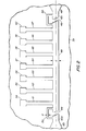
- Fig. 2 shows, in part, an actual convolver built using the invention on a substrate 39.
- Throats 40c and 42c of tapered horns 40 and 42 are shown communicating across gaps 44 and 46, respectively with interaction channel 48.
- horns 40 and 42 are shown truncated they are actually similar to the tapered parabolic horns of Fig. 1 and that transducers similar to those of Fig. 1 are used at the inputs to the horns in the manner described above with respect to Fig. 1.
- the bias cut of gaps 44 and 46 is stepped, in three distinct steps, rather than the smooth bias gap of Fig. 1, again to reduce coherent reflections from the ends of the horns and interaction region.
- Interaction channel 48 in this embodiment, has a plurality of equally spaced output ports 54 to 60 which are disposed respectively on branches 61 to 68 extending at a right angle from the side of interaction channel 48.
- use of such plurality of output ports, at which results of the convolution being performed in interaction channel 48 appear during the convolution, allows a more uniform convolution output signal as a function of distance along the interaction channel.
- Microstrip loops 50 and 52 are provided as electrical shunts across gaps 44 and 46, respectively. These loops, of course, are deposited on the substrate simultaneously with the rest of the microstrip components comprising the convolver, as explained above, and eliminate substrate cracks in the gap area.
- the width of interaction channel 48 that is dimension C, is about 32 um, while the width of a typical loop, for example, diameter D, is about 10 um. These dimensions provide a convolver output impedance of about 50 ohms and a loop resistance of about 150 ohms, a relationship that causes no significant effect on convolver performance if the loop is left intact in a permanent part of the convolver.
- Fig. 3 shows a portion of a convolver structure disposed on substrate 70.
- the convolver structure shown comprises thin film parabolic horn 72 having throat 72a, and thin film interaction channel 74, having output ports 76 and 78 disposed on arms 80 and 82, respectively.
- stepped gap 90 is provided between horn 72 and interaction channel 74 across which surface acoustic waves traversing horn 72 along longitutinal axis 68 are coupled to interaction channel 74.
- a thin film loop 84 electrically shunts gap 90.
- Loop 84 consists of legs 84a and 84b at right angles to longitudinal axis 68 and a thin film section 84c connecting the ends thereof.
- leg 84b is also branch or arm 82 for port 78. This scheme of using a port branch for a portion of the loop can be used when the port is located close to the gap.
Landscapes
- Physics & Mathematics (AREA)
- Acoustics & Sound (AREA)
- Surface Acoustic Wave Elements And Circuit Networks Thereof (AREA)
Applications Claiming Priority (2)
| Application Number | Priority Date | Filing Date | Title |
|---|---|---|---|
| US06/404,785 US4410824A (en) | 1982-08-03 | 1982-08-03 | Means for preventing cracks in the gap region of a surface acoustic wave device |
| US404785 | 1995-03-15 |
Publications (2)
| Publication Number | Publication Date |
|---|---|
| EP0100739A2 true EP0100739A2 (de) | 1984-02-15 |
| EP0100739A3 EP0100739A3 (de) | 1987-01-28 |
Family
ID=23601021
Family Applications (1)
| Application Number | Title | Priority Date | Filing Date |
|---|---|---|---|
| EP83401595A Withdrawn EP0100739A3 (de) | 1982-08-03 | 1983-08-02 | Akustische Oberflächenwellenanordnung und deren Herstellungsverfahren |
Country Status (3)
| Country | Link |
|---|---|
| US (1) | US4410824A (de) |
| EP (1) | EP0100739A3 (de) |
| JP (1) | JPS5949010A (de) |
Cited By (1)
| Publication number | Priority date | Publication date | Assignee | Title |
|---|---|---|---|---|
| EP2393124A4 (de) * | 2009-02-02 | 2013-07-31 | Lg Chemical Ltd | Rückseitige folie einer solarzelle und verfahren zu ihrer herstellung |
Families Citing this family (3)
| Publication number | Priority date | Publication date | Assignee | Title |
|---|---|---|---|---|
| WO1982001790A1 (en) * | 1980-11-17 | 1982-05-27 | Lewis Meirion F | Improvements in or relating to methods of producing devices comprising metallised regions on dielectric substrates |
| KR860000162B1 (ko) * | 1984-05-14 | 1986-02-27 | 금성계전 주식회사 | 탄성표면파 장치 |
| JPH08288787A (ja) * | 1995-04-10 | 1996-11-01 | Canon Inc | 弾性表面波素子装置、スペクトラム拡散通信装置およびこれを用いたシステム |
Family Cites Families (5)
| Publication number | Priority date | Publication date | Assignee | Title |
|---|---|---|---|---|
| US3840825A (en) * | 1973-08-03 | 1974-10-08 | Hughes Aircraft Co | Composite acoustic surface wave devices with bridge-like coupling film |
| US4063202A (en) * | 1976-05-05 | 1977-12-13 | Rockwell International Corporation | Band-pass filter with surface acoustic wave devices |
| US4181904A (en) * | 1978-08-09 | 1980-01-01 | The United States Of America As Represented By The Secretary Of The Navy | Acoustic-wave convolvers utilizing diffused waveguides and beam compression techniques |
| JPS55157321U (de) * | 1979-04-02 | 1980-11-12 | ||
| GB2088167B (en) * | 1980-11-17 | 1984-06-20 | Secr Defence | Preventing damaging electric fields eg in saw devices |
-
1982
- 1982-08-03 US US06/404,785 patent/US4410824A/en not_active Expired - Fee Related
-
1983
- 1983-08-02 EP EP83401595A patent/EP0100739A3/de not_active Withdrawn
- 1983-08-02 JP JP58141802A patent/JPS5949010A/ja active Pending
Cited By (1)
| Publication number | Priority date | Publication date | Assignee | Title |
|---|---|---|---|---|
| EP2393124A4 (de) * | 2009-02-02 | 2013-07-31 | Lg Chemical Ltd | Rückseitige folie einer solarzelle und verfahren zu ihrer herstellung |
Also Published As
| Publication number | Publication date |
|---|---|
| EP0100739A3 (de) | 1987-01-28 |
| US4410824A (en) | 1983-10-18 |
| JPS5949010A (ja) | 1984-03-21 |
Similar Documents
| Publication | Publication Date | Title |
|---|---|---|
| US4353046A (en) | Surface acoustic wave device with reflectors | |
| EP0481733A1 (de) | Akustischer Oberflächenwellenresonator | |
| CA1180436A (en) | Surface acoustic wave resonator device | |
| US4006438A (en) | Electro-acoustic surface-wave filter device | |
| JPH0559609B1 (de) | ||
| EP0026114B1 (de) | Vorrichtung mit akustischen Oberflächenwellen | |
| EP0147863B1 (de) | Akustischer Oberflächenwellenwandler | |
| CA1177126A (en) | Piezoelectric elastic-wave convolver device | |
| US5977846A (en) | Unidirectional surface acoustic wave filter | |
| KR20010101541A (ko) | 탄성파 장치 | |
| US3955159A (en) | Acoustic surface wave devices | |
| US4237433A (en) | Surface acoustic wave resonators with integrated internal coupler reflectors | |
| US3972011A (en) | Surface elastic wave electromechanical device | |
| US4350963A (en) | Surface acoustic wave device | |
| US4814658A (en) | SAW device with continuous finger pattern | |
| US4410824A (en) | Means for preventing cracks in the gap region of a surface acoustic wave device | |
| US3870975A (en) | Surface wave transducer with reduced reflection coefficient | |
| EP0044732A2 (de) | Akustischer Oberflächenwellenwandler mit verbesserter Frequenzcharakteristik | |
| US5714830A (en) | Free edge reflective-type surface acoustic wave device | |
| US5434466A (en) | Acoustic wave filter with reduced bulk-wave scattering loss and method | |
| US4048594A (en) | Surface acoustic wave filter | |
| JP3196499B2 (ja) | 表面波共振子 | |
| EP0057598A2 (de) | Akustische Oberflächenwellenvorrichtung | |
| JP2685537B2 (ja) | 弾性表面波装置、その製作方法、その調整方法、及びそれを用いた通信装置 | |
| US4206426A (en) | Multiple pole surface wave acoustic filters employing angled grooved distributed reflector arrays |
Legal Events
| Date | Code | Title | Description |
|---|---|---|---|
| PUAI | Public reference made under article 153(3) epc to a published international application that has entered the european phase |
Free format text: ORIGINAL CODE: 0009012 |
|
| AK | Designated contracting states |
Designated state(s): DE FR GB IT |
|
| PUAL | Search report despatched |
Free format text: ORIGINAL CODE: 0009013 |
|
| AK | Designated contracting states |
Kind code of ref document: A3 Designated state(s): DE FR GB IT |
|
| STAA | Information on the status of an ep patent application or granted ep patent |
Free format text: STATUS: THE APPLICATION IS DEEMED TO BE WITHDRAWN |
|
| 18D | Application deemed to be withdrawn |
Effective date: 19870929 |
|
| RIN1 | Information on inventor provided before grant (corrected) |
Inventor name: STEINBERG, RONALD FREDERICK |