EP0100817A2 - Boîtier à scellement hermétique pour un élément électrique et procédé de fabrication - Google Patents
Boîtier à scellement hermétique pour un élément électrique et procédé de fabrication Download PDFInfo
- Publication number
- EP0100817A2 EP0100817A2 EP83104133A EP83104133A EP0100817A2 EP 0100817 A2 EP0100817 A2 EP 0100817A2 EP 83104133 A EP83104133 A EP 83104133A EP 83104133 A EP83104133 A EP 83104133A EP 0100817 A2 EP0100817 A2 EP 0100817A2
- Authority
- EP
- European Patent Office
- Prior art keywords
- metal
- copper
- alloy
- base member
- refractory oxide
- Prior art date
- Legal status (The legal status is an assumption and is not a legal conclusion. Google has not performed a legal analysis and makes no representation as to the accuracy of the status listed.)
- Granted
Links
Images
Classifications
-
- H—ELECTRICITY
- H10—SEMICONDUCTOR DEVICES; ELECTRIC SOLID-STATE DEVICES NOT OTHERWISE PROVIDED FOR
- H10W—GENERIC PACKAGES, INTERCONNECTIONS, CONNECTORS OR OTHER CONSTRUCTIONAL DETAILS OF DEVICES COVERED BY CLASS H10
- H10W95/00—Packaging processes not covered by the other groups of this subclass
-
- H—ELECTRICITY
- H10—SEMICONDUCTOR DEVICES; ELECTRIC SOLID-STATE DEVICES NOT OTHERWISE PROVIDED FOR
- H10W—GENERIC PACKAGES, INTERCONNECTIONS, CONNECTORS OR OTHER CONSTRUCTIONAL DETAILS OF DEVICES COVERED BY CLASS H10
- H10W76/00—Containers; Fillings or auxiliary members therefor; Seals
- H10W76/10—Containers or parts thereof
- H10W76/12—Containers or parts thereof characterised by their shape
- H10W76/13—Containers comprising a conductive base serving as an interconnection
- H10W76/134—Containers comprising a conductive base serving as an interconnection having other interconnections parallel to the conductive base
-
- H—ELECTRICITY
- H10—SEMICONDUCTOR DEVICES; ELECTRIC SOLID-STATE DEVICES NOT OTHERWISE PROVIDED FOR
- H10W—GENERIC PACKAGES, INTERCONNECTIONS, CONNECTORS OR OTHER CONSTRUCTIONAL DETAILS OF DEVICES COVERED BY CLASS H10
- H10W76/00—Containers; Fillings or auxiliary members therefor; Seals
- H10W76/60—Seals
-
- H—ELECTRICITY
- H10—SEMICONDUCTOR DEVICES; ELECTRIC SOLID-STATE DEVICES NOT OTHERWISE PROVIDED FOR
- H10W—GENERIC PACKAGES, INTERCONNECTIONS, CONNECTORS OR OTHER CONSTRUCTIONAL DETAILS OF DEVICES COVERED BY CLASS H10
- H10W72/00—Interconnections or connectors in packages
- H10W72/50—Bond wires
- H10W72/551—Materials of bond wires
- H10W72/552—Materials of bond wires comprising metals or metalloids, e.g. silver
- H10W72/5524—Materials of bond wires comprising metals or metalloids, e.g. silver comprising aluminium [Al]
-
- H—ELECTRICITY
- H10—SEMICONDUCTOR DEVICES; ELECTRIC SOLID-STATE DEVICES NOT OTHERWISE PROVIDED FOR
- H10W—GENERIC PACKAGES, INTERCONNECTIONS, CONNECTORS OR OTHER CONSTRUCTIONAL DETAILS OF DEVICES COVERED BY CLASS H10
- H10W72/00—Interconnections or connectors in packages
- H10W72/851—Dispositions of multiple connectors or interconnections
- H10W72/874—On different surfaces
- H10W72/884—Die-attach connectors and bond wires
Definitions
- the invention is subject to a wide range of applications, it is especially suited for providing an article and a method of encasing a semiconductor and more particularly for providing a highly reliable hermetically sealed casing with a window frame device to allow for relatively low temperature packaging after the semiconductor device is installed.
- Hermetically sealed packages are used in applications in which maximum reliability is required. This is usually accomplished with ceramics or metals which are impervious to water vapor or other contaminants in the package together with sealing glasses which are also impervious to diffusion. Characteristically, the present hermetic packages cost much more than a plastic package, generally in the order of ten times greater.
- the present technology In producing a hermetically sealed package, the present technology often uses the following sequence of operations.
- a preformed and prefired ceramic substrate is provided.
- a metallized spot is applied to the center of this substrate to provide for later attachment of a semiconductor chip.
- the metallized spot is gold and the ceramic is normally aluminum oxide (alumina).
- the ceramic substrate may be produced from beryllium oxide. However, this is usually avoided because of the very high cost of beryllium oxide ceramics.
- a layer of sealing glass is silk screened as a paste around the periphery of the substrate.
- a lead frame is placed upon the glass and the resulting subassembly is passed through a furnace so that the glass fuses, bonding to the ceramic as well as to the lead frame.
- the lead frame material is striped with aluminum in its central area to provide an aluminum surface where lead wires are to be subsequently bonded.
- a low expansivity metal alloy such as 42 nickel-58 iron is used for the lead frame.
- These alloys are chosen because it is quite advantageous for the coefficient of thermal expansion of the alloy to approximately match that of the ceramic.
- the glass in turn is selected to provide a coefficient of thermal expansion comparable to that of the 42 nickel alloy and the ceramic. Close matching of coefficients of thermal expansion is required in order to maintain bond integrity and/or to avoid fracture of the glass. Either or both of these failures may result from the stresses developed while the package is cooling from the sealing temperature.
- Glass sealing alloys such as the 42 nickel alloy are relatively expensive. Their cost is approximately twice the cost of normal copper alloys. Furthermore, the thermal and, electrical conductivity of the typical glass sealing alloys is relatively low, approximately 4% that of pure copper.
- Alloy 6381 has about 10% the thermal conductivity of pure copper.
- the chip is now bonded to the metallized spot on the substrate using a standard gold-silicon eutectic braze bonding technique.
- the interconnection between the chip and the lead frame may be made by bonding small diameter lead wires between the two.
- sealing glass is silk screened upon the surface of the upper ceramic component.
- the upper component is placed over the previous subassembly and again fired so as to fuse the glass which bonds the package together into a single hermetic unit.
- U.S. Patent No. 3,340,602 to Hontz discloses, for example, "...the invention contemplates, in preferred practice thereof, the use of a gold-tin alloy soldier, preferably 20% tin by weight, to solder bond a gold plated cap to a gold plated housing within which there is disposed a silicon semi-conductive device comprising gold-to-aluminum solder connections.”
- U.S. Patent No. 3,435,516 to Kilby discloses, for example, "...methods of fabricating packages for semiconductor devices and methods for mounting and/or sealing bars of thin semiconductive materials having various circuit connections and terminals formed thereon.”
- U.S. Patent No. 3,546,363 to Pryor et al. discloses a composite metal product for'use as a seal to glasses and ceramics which has properties of a low coefficient of expansion, approximating that of the appropriate glasses and ceramics, good thermal conductivity, and fine grain size in the a nealed condition.
- U.S. Patent Nos. 3,546,363; 3,618,203; 3,676,292; 3 , 72 6, 9 8 7 ; 3 ,8 2 6,6 27 ; 3 ,8 2 6,6 29 ; 3,837,895; 3 ,8 52 , 1 48; and 4,149,910 disclose glass or ceramic t: metal composites or seals wherein the glass or ceramic is bonded to a base alloy having a thin film of refractory oxide on its surface.
- This casing includes a lead frame having an electrical device affixed thereto.
- a base member is glass bonded to a matching surface of the lead frame.
- a metal window frame shaped device is provided having one surface with a refractory oxide coating and a second opposite readily solderable surface.
- the refractory oxide layer of the window frame device is glass bonded to the lead frame.
- the semiconductor or electrical device is connected to the lead frame after the window frame has been glass bonded into place.
- a metal lid having a solderable surface is solder bonded to the solderable surface of the window frame to hermetically seal the electrical device within the casing.
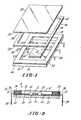
- Figure 1 is an exploded view of the elements of a hermetically sealed semiconductor casing adapted for assembly in accordance with the present invention.
- Figure 2 is a side view in cross section of a hermetically sealed semiconductor casing in accordance with the present invention.
- a metal or metal alloy lead frame 14 has first and second opposite surfaces 16 and 18 and the electrical device or chip 12 affixed thereto.
- a metal or metal alloy base member has a surface 22 which is bonded by glass 24 to the second surface 18 of the lead frame.
- a metal or metal alloy window frame shaped device 26 has at least a first surface 28 with a refractory oxide coating (not illustrated).
- the window frame 26 also has a second opposite surface 30 which is readily solderable.
- a metal or metal alloy lid or cover 32 has at least a first readily solderable surface 34. Solder 36 is interposed between the second surface 30 of the window frame device and the first surface 34 of the lid 32 so that the electrical component 12 is substantially hermetically sealed within the casing 10.
- the metal substrate or base member 20 may consist primarily of a high thermal conductivity metal or metal alloy such as for example copper or aluminum metals or alloys.
- the high conductivity metal or alloy substrate may be campletely formed or preferably clad with a thin layer 40 of any desired metal or alloy which bonds strongly with a glass bonding agent.
- the preferred metal or alloy of the present invention which bonds with a glass bonding agent has a thin refractory oxide layer on its- surface.
- the preferred alloy is a copper base alloy containing from 2 to 12% aluminum and the balance copper.
- the alloy contains from 2 to 10% aluminum, 0.001 to 3% silicon and, if desired, a grain refining element selected from the group consisting of iron up to 4.5%, chromium up to 1%, zirconium up to 0.5%, cobalt up to 1% and mixtures of these grain refining elements and the balance copper.
- a grain refining element selected from the group consisting of iron up to 4.5%, chromium up to 1%, zirconium up to 0.5%, cobalt up to 1% and mixtures of these grain refining elements and the balance copper.
- CDA alloy C6381 containing 2.5 to 3.1% aluminum, 1.5 to 2.1% silicon, and the balance copper is useful as a substrate layer 40 for this invention.
- CDA alloy C638, as disclosed in U.S. Patent No. 3,676,292 to Pryor et al. is suitable. Alloy C638 is similar to C6381 except for the addition of cobalt. Impurities may be present in either alloy which do not prevent bonding in
- CDA alloy C6381 as described in U.S. Patent Nos. 3,341,.369 and 3,475,227 to Caule et al. which disclose copper base alloys and processes for preparing them, have a refractory oxide layer formed to one or more of their surfaces.
- the oxide layer may include complex oxides formed with elements such as alumina, silica, tin, iron chromia, zinc, and manganese.
- the refractory oxide layer is substantially aluminum oxide (A1 2 0 3 ).
- the formation of the refractory oxide to the substrate may be accomplished in any desired manner.
- a copper base alloy such as alloy C6381 may be preoxidized in gases having an extremely low oxygen content.
- the C6381 may be placed in. a container with 4% hydrogen, 96% nitrogen and a trace of oxygen released from a trace of water mixed in the gas.
- This gas may be heated to a temperature of between about 330°C and about 820°C.
- a refractory oxide layer of a desired thickness forms on the surface of the alloy.
- alloy C6381 includes the broad field of metal or alloys which have the ability to form continuous refractory oxide layers on their surface.
- metal alloys such as nickel base and iron base alloys are disclosed in U.S. Patent Nos. 3,698,964, 3,730,779 and 3,810,754.
- Alloy C6381 is particularly suitable for this invention because it is a commercial alloy which forms such films when heated.
- the lead frame 14 is also constructed of a metal or alloy, as described above, which bonds well to glass.
- the lead frame is formed of C6381 and has a refractory oxide formed on surfaces 16 and 18.
- the terminal leads 38 project through the glass component 24 external to the casing 30.
- the terminal leads preferably protrude from two sides of the casing, it is within the scope of the present invention for the terminal leads to extend from any number of sides.
- the present invention uses any suitable solder glass or ceramic 24 preferably having a coefficient of thermal expansion/contraction which closely matches the metal components.
- the glass may be bonded to the thin refractory oxide surface layers on component 40 and lead frame 14 and functions to adhere the metal components together and electrically insulate them from each other.
- thermal stresses i 11 the system may be essentially eliminated and the problems associated with thermal stress in the finished product alleviated.
- the specific character of the refractory oxide layer present on the preferred alloys C638 or C6381 allows bonding to solder glasses with significantly lower expansion/contraction coefficients than that of the alloy. It has been demonstrated that mechanically sound bonds can be achieved between C638 and CV432 (contraction coefficient of 127 x 10-7°C).
- Table I lists various exemplary solder glasses which are adapted for use in accordance with this invention.
- the window frame shaped element 26 may be formed of a composite of a metal or alloy having a refractory oxide layer on one surface such as for example CDA alloy C6381 or any other metal or alloy having the ability to form continuous refractory oxide layers on their surface as mentioned hereinabove. This allows the window frame to be securely bonded to glass 24 in a conventional manner.
- the window frame may be formed of a single metal or alloy, it is preferably provided with a cladding 42 of a more readily solderable alloy such as CDA alloy C151.
- the lid or top cover 32 is also fabricated from a suitable solderable metal or alloy, such as for example a copper or aluminum metal or alloy, preferably CDA alloy C151, as described above. However, it is within the scope of the present invention to use any solderable metal or alloy to form the lid 32 or component 42 of the window frame 26.
- a suitable solderable metal or alloy such as for example a copper or aluminum metal or alloy, preferably CDA alloy C151, as described above.
- any solderable metal or alloy to form the lid 32 or component 42 of the window frame 26.
- the advantage of having the opposing surfaces 34 and 30 of the lid 32 and the window frame 26, respectively, to be readily solderable permits the use of much less expensive. solders and eliminates the need to gold plate the components as in the prior art.
- the solder 36 may be comprised of any conventional solder depending on the requirements of the application. For example, if there is a need to avoid flux, a gold-tin solder mixture might b:e desirable. Also, in an application having a low temperature restraint, a lead-tin solder might be desirable.
- the semiconductor chip 12 is bonded to the pad 50 of the lead frame 14. This bonding may be accomplished by either using a conductive adhesive as is often the case in integrated circuits or a relatively low melting temperature solder.
- the plastic adhesives include epoxies and polyimides. They may be formulated with powdered metals, such as silver, to improve their thermal conductivity and/or to provide moderate electrical conductivity.
- the metal joining materials may include a gold-tin or lead-tin eutectic solder. In addition, it is within the scope of the present invention to use any desired solder or other bonding technique as required.
- the interconnection between the chip 12 and the lead frame 14 is typically provided by means of small diameter lead wires 52 (usually gold) which are metallurgically bonded to the tips of the leads in the lead frame and to the chip.
- the bonding technique is preferably either thermosonic or thermocompression bonding.
- Thermosonic bonding is a combination of mechanically induced metallurgical bonding at temperatures above ambient in conjunction with the addition of ultrasonic energy.
- Thermocompression bonding is mechanical deformation at elevated temperature without the addition of the ultrasonic energy.
- a foil "spider" is often -used as an alternative to the wires.
- the foil itself may be bonded to the chip by either thermosonic or thermocompression bonding.
- the lead frame 14 is glass sealed with glass 24 to the refractory oxide surface as cladding 40 of base member 20.
- the window frame shaped device has its refractory oxide coated surface 28 bonded to the glass 24 which is bonding the lead frame to the metal substrate.
- the glass may actually be between the metal substrate and the window frame in areas not covered by the lead frame. _Although these steps are disclosed as being separate, they may actually be performed concurrently. Now that the high temperature operations are concluded, the semiconductor chip 12 is mounted upon the pad 50.
- the chip By removing the need to subject the package to relatively high glass sealing temperatures, the chip may be attached to the substrate with a relatively low melting temperature solder or even an organic adhesive. In either case, the problems associated with the mismatch in thermal conductivity between the chip and the pad are minimized. This is due to the fact that the temperature difference between the chip bonding temperature and the ambient temperature is substantially less than in the case of gold-silicon eutectic braze bonding as is often required in conventional hermetically sealed semiconductor casings.
- the wires 52 between the lead frame and the chip may be thermocompression or thermosonically bonded. This can eliminate the slower ultrasonic wire bonding used in glass sealed hermetic packages since the final closure using relatively low temperature solder does not have a substantial adverse effect on the bonding wires 52.
- a lid or cover 32 is soldered to the window frame to hermetically seal the semiconductor device in the casing 10.
- the surfaces which are soldered are preferably formed of a readily solderable copper alloy which permits the use of relatively inexpensive solders and eliminates the need to gold plate the soldered components.
- the solderable metals, as described above, are characteristically substantially less costly than the low expansivity alloys which are frequently used in the present technology.
Landscapes
- Lead Frames For Integrated Circuits (AREA)
- Cooling Or The Like Of Semiconductors Or Solid State Devices (AREA)
- Joining Of Glass To Other Materials (AREA)
Applications Claiming Priority (2)
| Application Number | Priority Date | Filing Date | Title |
|---|---|---|---|
| US40564082A | 1982-08-05 | 1982-08-05 | |
| US405640 | 1982-08-05 |
Publications (3)
| Publication Number | Publication Date |
|---|---|
| EP0100817A2 true EP0100817A2 (fr) | 1984-02-22 |
| EP0100817A3 EP0100817A3 (en) | 1986-01-22 |
| EP0100817B1 EP0100817B1 (fr) | 1989-04-05 |
Family
ID=23604557
Family Applications (1)
| Application Number | Title | Priority Date | Filing Date |
|---|---|---|---|
| EP83104133A Expired EP0100817B1 (fr) | 1982-08-05 | 1983-04-27 | Boîtier à scellement hermétique pour un élément électrique et procédé de fabrication |
Country Status (4)
| Country | Link |
|---|---|
| EP (1) | EP0100817B1 (fr) |
| JP (1) | JPS5933851A (fr) |
| CA (1) | CA1201211A (fr) |
| DE (1) | DE3379562D1 (fr) |
Cited By (7)
| Publication number | Priority date | Publication date | Assignee | Title |
|---|---|---|---|---|
| EP0164794A3 (en) * | 1984-06-14 | 1987-03-04 | Monolithic Memories, Inc. | Multi-layer heat sinking integrated circuit package |
| EP0178481A3 (en) * | 1984-09-19 | 1987-12-23 | Olin Corporation | Hermetically sealed semiconductor package |
| EP0379431A1 (fr) * | 1989-01-20 | 1990-07-25 | Dassault Electronique | Procédé de scellement verre-aluminium, notamment pour traversée électrique de boîtier de circuit hybride, objet composite et composition de verre correspondants |
| FR2648275A1 (fr) * | 1989-06-09 | 1990-12-14 | Thomson Csf | Procede et dispositif d'encapsulation de modules hyperfrequence |
| EP0485627A4 (en) * | 1990-05-31 | 1993-06-02 | Kabushiki Kaisha Toshiba | Lead frame and semiconductor package using it |
| EP0700083A3 (fr) * | 1988-10-05 | 1996-04-10 | Olin Corp | |
| WO2009144224A1 (fr) * | 2008-05-27 | 2009-12-03 | Epcos Ag | Boîtier hermétiquement clos pour composants électroniques et son procédé de fabrication |
Family Cites Families (6)
| Publication number | Priority date | Publication date | Assignee | Title |
|---|---|---|---|---|
| FR1284534A (fr) * | 1959-05-06 | 1962-02-16 | Texas Instruments Inc | Fabrication de dispositifs semi-conducteurs |
| US3381080A (en) * | 1962-07-02 | 1968-04-30 | Westinghouse Electric Corp | Hermetically sealed semiconductor device |
| US3340602A (en) * | 1965-02-01 | 1967-09-12 | Philco Ford Corp | Process for sealing |
| US3546363A (en) * | 1967-01-11 | 1970-12-08 | Olin Corp | Composite glass-to-metal seal |
| GB1369627A (en) * | 1970-12-18 | 1974-10-09 | Hitachi Ltd | Method for manufacturing a printed ceramic substrate |
| DE3010076A1 (de) * | 1980-03-15 | 1981-09-24 | W.C. Heraeus Gmbh, 6450 Hanau | Halbzeug fuer die herstellung von metalldeckeln zum verschliessen von gehaeusen aus keramischem werkstoff |
-
1983
- 1983-04-26 CA CA000426743A patent/CA1201211A/fr not_active Expired
- 1983-04-27 DE DE8383104133T patent/DE3379562D1/de not_active Expired
- 1983-04-27 EP EP83104133A patent/EP0100817B1/fr not_active Expired
- 1983-06-02 JP JP58097027A patent/JPS5933851A/ja active Granted
Cited By (10)
| Publication number | Priority date | Publication date | Assignee | Title |
|---|---|---|---|---|
| EP0164794A3 (en) * | 1984-06-14 | 1987-03-04 | Monolithic Memories, Inc. | Multi-layer heat sinking integrated circuit package |
| EP0178481A3 (en) * | 1984-09-19 | 1987-12-23 | Olin Corporation | Hermetically sealed semiconductor package |
| EP0700083A3 (fr) * | 1988-10-05 | 1996-04-10 | Olin Corp | |
| EP0379431A1 (fr) * | 1989-01-20 | 1990-07-25 | Dassault Electronique | Procédé de scellement verre-aluminium, notamment pour traversée électrique de boîtier de circuit hybride, objet composite et composition de verre correspondants |
| FR2642257A1 (fr) * | 1989-01-20 | 1990-07-27 | Dassault Electronique | Procede de scellement verre-aluminium, notamment pour traversee electrique de boitier de circuit hybride, objet composite et composition de verre correspondants |
| US5538527A (en) * | 1989-01-20 | 1996-07-23 | Dassault Electronique | Method of sealing glass to aluminum, particularly for electrical feed-through connectors |
| FR2648275A1 (fr) * | 1989-06-09 | 1990-12-14 | Thomson Csf | Procede et dispositif d'encapsulation de modules hyperfrequence |
| EP0485627A4 (en) * | 1990-05-31 | 1993-06-02 | Kabushiki Kaisha Toshiba | Lead frame and semiconductor package using it |
| US5315152A (en) * | 1990-05-31 | 1994-05-24 | Kabushiki Kaisha Toshiba | Lead frame with improved adhesiveness property against plastic and plastic sealing type semiconductor packaging using said lead frame |
| WO2009144224A1 (fr) * | 2008-05-27 | 2009-12-03 | Epcos Ag | Boîtier hermétiquement clos pour composants électroniques et son procédé de fabrication |
Also Published As
| Publication number | Publication date |
|---|---|
| EP0100817B1 (fr) | 1989-04-05 |
| JPS5933851A (ja) | 1984-02-23 |
| EP0100817A3 (en) | 1986-01-22 |
| JPH0263308B2 (fr) | 1990-12-27 |
| CA1201211A (fr) | 1986-02-25 |
| DE3379562D1 (en) | 1989-05-11 |
Similar Documents
| Publication | Publication Date | Title |
|---|---|---|
| US4656499A (en) | Hermetically sealed semiconductor casing | |
| US4784974A (en) | Method of making a hermetically sealed semiconductor casing | |
| US4542259A (en) | High density packages | |
| US4577056A (en) | Hermetically sealed metal package | |
| US5001546A (en) | Clad metal lead frame substrates | |
| US4897508A (en) | Metal electronic package | |
| US4461924A (en) | Semiconductor casing | |
| US4524238A (en) | Semiconductor packages | |
| US4363076A (en) | Integrated circuit package | |
| US4727633A (en) | Method of securing metallic members together | |
| US4480262A (en) | Semiconductor casing | |
| US4594770A (en) | Method of making semiconductor casing | |
| EP0097833B1 (fr) | Substrat pour empaquetages de circuits intégrés | |
| EP0084866A2 (fr) | Boîtier pour semi-conducteur | |
| US4682414A (en) | Multi-layer circuitry | |
| US4827377A (en) | Multi-layer circuitry | |
| EP0100817B1 (fr) | Boîtier à scellement hermétique pour un élément électrique et procédé de fabrication | |
| JPS5873904A (ja) | 銀充填ガラス | |
| IE54534B1 (en) | Semiconductor device package | |
| IE53305B1 (en) | Silver-filled glass | |
| JP2740605B2 (ja) | 半導体素子収納用パッケージの製造方法 | |
| JPS6175548A (ja) | 半導体装置 | |
| CA1304172C (fr) | Boitier metallique pour dispositif electronique | |
| JPS5961054A (ja) | 半導体装置 | |
| JPH0341475Y2 (fr) |
Legal Events
| Date | Code | Title | Description |
|---|---|---|---|
| PUAI | Public reference made under article 153(3) epc to a published international application that has entered the european phase |
Free format text: ORIGINAL CODE: 0009012 |
|
| AK | Designated contracting states |
Designated state(s): DE FR GB IT NL |
|
| PUAL | Search report despatched |
Free format text: ORIGINAL CODE: 0009013 |
|
| AK | Designated contracting states |
Designated state(s): DE FR GB IT NL |
|
| 17P | Request for examination filed |
Effective date: 19860721 |
|
| 17Q | First examination report despatched |
Effective date: 19870701 |
|
| ITF | It: translation for a ep patent filed | ||
| GRAA | (expected) grant |
Free format text: ORIGINAL CODE: 0009210 |
|
| AK | Designated contracting states |
Kind code of ref document: B1 Designated state(s): DE FR GB IT NL |
|
| REF | Corresponds to: |
Ref document number: 3379562 Country of ref document: DE Date of ref document: 19890511 |
|
| ET | Fr: translation filed | ||
| PLBE | No opposition filed within time limit |
Free format text: ORIGINAL CODE: 0009261 |
|
| STAA | Information on the status of an ep patent application or granted ep patent |
Free format text: STATUS: NO OPPOSITION FILED WITHIN TIME LIMIT |
|
| 26N | No opposition filed | ||
| ITTA | It: last paid annual fee | ||
| PGFP | Annual fee paid to national office [announced via postgrant information from national office to epo] |
Ref country code: FR Payment date: 19930316 Year of fee payment: 11 |
|
| PGFP | Annual fee paid to national office [announced via postgrant information from national office to epo] |
Ref country code: GB Payment date: 19930322 Year of fee payment: 11 |
|
| PGFP | Annual fee paid to national office [announced via postgrant information from national office to epo] |
Ref country code: NL Payment date: 19930430 Year of fee payment: 11 |
|
| PGFP | Annual fee paid to national office [announced via postgrant information from national office to epo] |
Ref country code: DE Payment date: 19930630 Year of fee payment: 11 |
|
| PG25 | Lapsed in a contracting state [announced via postgrant information from national office to epo] |
Ref country code: GB Effective date: 19940427 |
|
| PG25 | Lapsed in a contracting state [announced via postgrant information from national office to epo] |
Ref country code: NL Effective date: 19941101 |
|
| NLV4 | Nl: lapsed or anulled due to non-payment of the annual fee | ||
| GBPC | Gb: european patent ceased through non-payment of renewal fee |
Effective date: 19940427 |
|
| PG25 | Lapsed in a contracting state [announced via postgrant information from national office to epo] |
Ref country code: FR Effective date: 19941229 |
|
| PG25 | Lapsed in a contracting state [announced via postgrant information from national office to epo] |
Ref country code: DE Effective date: 19950103 |
|
| REG | Reference to a national code |
Ref country code: FR Ref legal event code: ST |