EP0101630A1 - Verfahren und System zum Einkapseln elektronischer Bauteile in Kunststoff - Google Patents
Verfahren und System zum Einkapseln elektronischer Bauteile in Kunststoff Download PDFInfo
- Publication number
- EP0101630A1 EP0101630A1 EP83201115A EP83201115A EP0101630A1 EP 0101630 A1 EP0101630 A1 EP 0101630A1 EP 83201115 A EP83201115 A EP 83201115A EP 83201115 A EP83201115 A EP 83201115A EP 0101630 A1 EP0101630 A1 EP 0101630A1
- Authority
- EP
- European Patent Office
- Prior art keywords
- mould
- strip
- elements
- plastic material
- plastic
- Prior art date
- Legal status (The legal status is an assumption and is not a legal conclusion. Google has not performed a legal analysis and makes no representation as to the accuracy of the status listed.)
- Granted
Links
Images
Classifications
-
- H—ELECTRICITY
- H10—SEMICONDUCTOR DEVICES; ELECTRIC SOLID-STATE DEVICES NOT OTHERWISE PROVIDED FOR
- H10W—GENERIC PACKAGES, INTERCONNECTIONS, CONNECTORS OR OTHER CONSTRUCTIONAL DETAILS OF DEVICES COVERED BY CLASS H10
- H10W74/00—Encapsulations, e.g. protective coatings
- H10W74/01—Manufacture or treatment
- H10W74/016—Manufacture or treatment using moulds
-
- B—PERFORMING OPERATIONS; TRANSPORTING
- B29—WORKING OF PLASTICS; WORKING OF SUBSTANCES IN A PLASTIC STATE IN GENERAL
- B29C—SHAPING OR JOINING OF PLASTICS; SHAPING OF MATERIAL IN A PLASTIC STATE, NOT OTHERWISE PROVIDED FOR; AFTER-TREATMENT OF THE SHAPED PRODUCTS, e.g. REPAIRING
- B29C45/00—Injection moulding, i.e. forcing the required volume of moulding material through a nozzle into a closed mould; Apparatus therefor
- B29C45/14—Injection moulding, i.e. forcing the required volume of moulding material through a nozzle into a closed mould; Apparatus therefor incorporating preformed parts or layers, e.g. injection moulding around inserts or for coating articles
- B29C45/14639—Injection moulding, i.e. forcing the required volume of moulding material through a nozzle into a closed mould; Apparatus therefor incorporating preformed parts or layers, e.g. injection moulding around inserts or for coating articles for obtaining an insulating effect, e.g. for electrical components
- B29C45/14655—Injection moulding, i.e. forcing the required volume of moulding material through a nozzle into a closed mould; Apparatus therefor incorporating preformed parts or layers, e.g. injection moulding around inserts or for coating articles for obtaining an insulating effect, e.g. for electrical components connected to or mounted on a carrier, e.g. lead frame
-
- B—PERFORMING OPERATIONS; TRANSPORTING
- B29—WORKING OF PLASTICS; WORKING OF SUBSTANCES IN A PLASTIC STATE IN GENERAL
- B29C—SHAPING OR JOINING OF PLASTICS; SHAPING OF MATERIAL IN A PLASTIC STATE, NOT OTHERWISE PROVIDED FOR; AFTER-TREATMENT OF THE SHAPED PRODUCTS, e.g. REPAIRING
- B29C45/00—Injection moulding, i.e. forcing the required volume of moulding material through a nozzle into a closed mould; Apparatus therefor
- B29C45/17—Component parts, details or accessories; Auxiliary operations
- B29C45/46—Means for plasticising or homogenising the moulding material or forcing it into the mould
- B29C45/462—Injection of preformed charges of material
Definitions
- the invention relates to a method for encapsulating parts of elements into a plastic material to manufacture electronic components, which parts are contained into one or more parallel rows into the mould cavities of a mould, into which plastic material is injected through one or more sprues.
- the invention now provides a method in which said elements are combined into a strip of which the length is a multiplicity of the length of a row of elements, which . strip is step by step treated in said mould such that an uninterrupted strip of components is obtained.
- moulds are used of the type described in the copending Dutch Patent Application 82,03255. It is however also conceivable to use the same method with a mould which does not comprise a hard layer or a mould having means assisting the release of the plastic material.
- the advantage of the invention is that automation is possible, that very short cycle periods can be realized with only a small amount of waste if each mould cavity has his own injection cylinder, for instance connected to the side edge of the row of moulds. If a predetermined plastic powder unit (pallet) is supplied through each injection cylinder, then the dosage of the amount of plastic per mould is very accurate whereas, as result of the positioning of the cylinder adjacent to the mould, a very short sprue is used.
- the plastic powder unit (pallet) therefore can have only a volume corresponding to the combined volume of the mould and the sprue. It is therefore possible to treat very small components and use very small amounts of plastic, especially in a mould which is coated with nitride.
- the invention furthermore relates to a system for carrying out the method according to the invention which system comprises at least one row of aligned adjoining mould cavities of a mould with two sections, which can be moved away from each other, which mould cavities have a mutual distance equal to the pitch between the elements of the supplied strip of elements, said system comprises means for step by step transporting said strip and for opening and closing said mould such that a section of said strip is enclosed into or released from said mould, said system comprises furthermore means to inject plastic material into the mould cavities.
- each mould cavity has an own plastic supplying device each connected to the side edge of the row of mould cavities. In that case very short sprues can be obtained.
- each supplying device has a press cylinder with a loading chamber which in the retracted position of the press piston of said cylinder offers space to a plastic powder unit of which the volume is equal to the volume of plastic to be injected and whereby furthermore the stroke of the piston of the press cylinder can be adjusted to compensate for differences in volume of the powder units and to adapt the volume to different moulds.
- a device can be installed which in tact with the operation of the mould cleans the components of the strip received from the mould by removing sprue elements not belonging to the encapsulating.
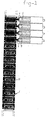
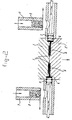
- a strip 1 of chip carrying elements 11 are positioned into a mould 2, for instance a mould as described in the copending Dutch Patent Application 82,03255, whereby the connecting pins of the elements are mutually turn and turn dislocated.
- the plastic material 3 is brought into the loading chamber in the form of pills through the supply unit 7.
- the powder unit in the form of a pill, brought into the supply unit 7 is fluidized because the adjoining mould parts 2 and 2' are heated whereafter the plastic material is through the sprue 4 injected into the mould cavity 6, in which mould cavity 6 the parts of the strip 1 to be encapsulated are positioned.
- the stroke volume of the piston 8 is adjustable the injected amount of plastic encapsulating the element in the mould can be adjusted. After hardening and releasing from the mould an electronic component is obtained connected to a sprue element and to a lump of plastic remaining in the cylinder.
- Said sprue element has minimum dimensions and comprises a minimum amount of material, however, it is always necessary to work with a sprue because of changes in the grain size of the plastic powder, so that the volume cannot be determined with great accuracy. With the described method however one obtains the result that the dosage is more accurate than with the usual central injection system, resulting into a decreased material waste.
- the mould may comprise several sections with a length corresponding to the length of an element 11.
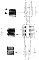
- Each mould has an own injection cylinder 5, schematically indicated in Fig. 3 with the reference number 9.
- Fig. 3 some devices in the neighbourhood of the injection device are illustrated.
- the chips or crystals and the connecting pins are mounted onto the strip at 8.
- the strip may be received from a supply reel and transported to the area 8, in which also bonding takes place, whereafter the strip is transported into the described device 9 for encapsulating into plastic. Thereafter the elements, encapsulated in the device 9, can be cleaned from the superfluous plastic, the sprue elements, into the device 10. Because as a result of the method according to the invention the encapsulating in plasic can take place continuously intermittent without the necessity to cut the strip into sections, also the supply of elements and the removal of the superfluous plastic can be carried out in a continuous (intermittent) way, so that an automized production can be realized.
Landscapes
- Engineering & Computer Science (AREA)
- Manufacturing & Machinery (AREA)
- Mechanical Engineering (AREA)
- Encapsulation Of And Coatings For Semiconductor Or Solid State Devices (AREA)
- Injection Moulding Of Plastics Or The Like (AREA)
Priority Applications (1)
| Application Number | Priority Date | Filing Date | Title |
|---|---|---|---|
| AT83201115T ATE26896T1 (de) | 1982-08-19 | 1983-07-27 | Verfahren und system zum einkapseln elektronischer bauteile in kunststoff. |
Applications Claiming Priority (2)
| Application Number | Priority Date | Filing Date | Title |
|---|---|---|---|
| NL8203253 | 1982-08-19 | ||
| NL8203253A NL8203253A (nl) | 1982-08-19 | 1982-08-19 | Werkwijze en inrichting voor het met kunststof omhullen van elektronische componenten. |
Publications (2)
| Publication Number | Publication Date |
|---|---|
| EP0101630A1 true EP0101630A1 (de) | 1984-02-29 |
| EP0101630B1 EP0101630B1 (de) | 1987-04-29 |
Family
ID=19840156
Family Applications (1)
| Application Number | Title | Priority Date | Filing Date |
|---|---|---|---|
| EP83201115A Expired EP0101630B1 (de) | 1982-08-19 | 1983-07-27 | Verfahren und System zum Einkapseln elektronischer Bauteile in Kunststoff |
Country Status (6)
| Country | Link |
|---|---|
| US (1) | US4653993A (de) |
| EP (1) | EP0101630B1 (de) |
| JP (1) | JPS5952842A (de) |
| AT (1) | ATE26896T1 (de) |
| DE (1) | DE3371263D1 (de) |
| NL (1) | NL8203253A (de) |
Cited By (2)
| Publication number | Priority date | Publication date | Assignee | Title |
|---|---|---|---|---|
| EP0201959A1 (de) * | 1985-05-14 | 1986-11-20 | Arbo Handels- En Ontwikkelingsmij B.V. | Vorrichtung zur gleichzeitigen Umhüllung von mehreren elektronischen Bauteilen |
| AT512441A1 (de) * | 2012-01-18 | 2013-08-15 | Engel Austria Gmbh | Verfahren zur herstellung eines faserverbund- oder hybridbauteils |
Families Citing this family (16)
| Publication number | Priority date | Publication date | Assignee | Title |
|---|---|---|---|---|
| DE3700902A1 (de) * | 1986-01-14 | 1987-07-16 | Mitsubishi Gas Chemical Co | Verfahren zur herstellung von plastikgeformten, gedruckten schaltplatten |
| JPH0740573B2 (ja) * | 1987-01-26 | 1995-05-01 | 株式会社東芝 | 半導体製造装置 |
| US5200125A (en) * | 1988-12-24 | 1993-04-06 | T&K International Laboratory, Ltd. | Method for seal molding electronic components with resin |
| US4927590A (en) * | 1989-05-26 | 1990-05-22 | At&T Bell Laboratories | Method for encapsulating integrated circuits |
| US6153141A (en) * | 1993-11-23 | 2000-11-28 | Motorola, Inc. | Semiconductor packaging method |
| JP3383701B2 (ja) * | 1994-03-07 | 2003-03-04 | 松下電器産業株式会社 | 樹脂封入成形用金型 |
| NL9400844A (nl) * | 1994-05-24 | 1996-01-02 | Boschman Holding Bv | Werkwijze en inrichting voor het ommantelen van voorwerpen. |
| US5855924A (en) * | 1995-12-27 | 1999-01-05 | Siemens Microelectronics, Inc. | Closed-mold for LED alphanumeric displays |
| JP2970569B2 (ja) * | 1997-01-13 | 1999-11-02 | 日本電気株式会社 | 樹脂封止方法および樹脂封止金型装置 |
| US5925384A (en) * | 1997-04-25 | 1999-07-20 | Micron Technology, Inc. | Manual pellet loader for Boschman automolds |
| US6666997B2 (en) * | 2001-10-02 | 2003-12-23 | Micron Technology, Inc. | Method for removing cleaning compound flash from mold vents |
| US7264456B2 (en) * | 2001-10-10 | 2007-09-04 | Micron Technology, Inc. | Leadframe and method for reducing mold compound adhesion problems |
| US7323361B2 (en) * | 2002-03-29 | 2008-01-29 | Fairchild Semiconductor Corporation | Packaging system for semiconductor devices |
| JP2004063851A (ja) * | 2002-07-30 | 2004-02-26 | Renesas Technology Corp | 樹脂封止装置 |
| KR20090006096A (ko) | 2006-04-11 | 2009-01-14 | 토와 가부시기가이샤 | 전자 부품의 수지 밀봉 성형 방법 및 전자 부품의 수지 밀봉 성형 장치 |
| US7678617B1 (en) | 2006-12-21 | 2010-03-16 | National Semiconductor Corporation | Universal laminator |
Citations (2)
| Publication number | Priority date | Publication date | Assignee | Title |
|---|---|---|---|---|
| FR2390008A1 (de) * | 1977-05-05 | 1978-12-01 | Fierkens Richardus | |
| EP0007762A1 (de) * | 1978-07-17 | 1980-02-06 | Dusan Slepcevic | Vorrichtung und Verfahren zum Umhüllen von elektronischen Bauteilen mit härtbarem Kunststoff |
Family Cites Families (13)
| Publication number | Priority date | Publication date | Assignee | Title |
|---|---|---|---|---|
| GB960097A (en) * | 1960-04-14 | 1964-06-10 | Dubilier Condenser Co 1925 Ltd | Improvements in or relating to the production of encapsulated electrical components |
| US3471900A (en) * | 1967-05-24 | 1969-10-14 | Trw Inc | Mold for encapsulating electrical components |
| IT982109B (it) * | 1973-04-27 | 1974-10-21 | Billi Spa | Sistema di comando degli aghi per macchine da maglieria con amplifi cazione del comando imposto dalle camme |
| US3915780A (en) * | 1973-08-02 | 1975-10-28 | Texas Instruments Inc | Extruded epoxy packaging system |
| US4109373A (en) * | 1975-03-10 | 1978-08-29 | General Electric Company | Method for manufacturing semiconductor devices |
| JPS5326670A (en) * | 1976-08-25 | 1978-03-11 | Hitachi Ltd | Manufacture of semiconductor device |
| JPS54162963A (en) * | 1978-06-14 | 1979-12-25 | Mitsubishi Electric Corp | Manufacture of resin-sealed semiconductor device |
| US4368168A (en) * | 1978-07-17 | 1983-01-11 | Dusan Slepcevic | Method for encapsulating electrical components |
| JPS5850582B2 (ja) * | 1979-08-24 | 1983-11-11 | 道男 長田 | 半導体封入成形方法とその金型装置 |
| JPS5649533A (en) * | 1979-09-28 | 1981-05-06 | Hitachi Ltd | Manufacture method of electron watch |
| JPS6045571B2 (ja) * | 1980-06-18 | 1985-10-11 | 株式会社東芝 | 樹脂封止用モ−ルド装置 |
| US4388265A (en) * | 1981-12-14 | 1983-06-14 | Kazuo Bandoh | Process and apparatus for molding plastics |
| US4460537A (en) * | 1982-07-26 | 1984-07-17 | Motorola, Inc. | Slot transfer molding apparatus and methods |
-
1982
- 1982-08-19 NL NL8203253A patent/NL8203253A/nl not_active Application Discontinuation
-
1983
- 1983-07-27 EP EP83201115A patent/EP0101630B1/de not_active Expired
- 1983-07-27 AT AT83201115T patent/ATE26896T1/de not_active IP Right Cessation
- 1983-07-27 DE DE8383201115T patent/DE3371263D1/de not_active Expired
- 1983-08-12 JP JP58148678A patent/JPS5952842A/ja active Pending
- 1983-08-16 US US06/523,749 patent/US4653993A/en not_active Expired - Fee Related
Patent Citations (2)
| Publication number | Priority date | Publication date | Assignee | Title |
|---|---|---|---|---|
| FR2390008A1 (de) * | 1977-05-05 | 1978-12-01 | Fierkens Richardus | |
| EP0007762A1 (de) * | 1978-07-17 | 1980-02-06 | Dusan Slepcevic | Vorrichtung und Verfahren zum Umhüllen von elektronischen Bauteilen mit härtbarem Kunststoff |
Cited By (4)
| Publication number | Priority date | Publication date | Assignee | Title |
|---|---|---|---|---|
| EP0201959A1 (de) * | 1985-05-14 | 1986-11-20 | Arbo Handels- En Ontwikkelingsmij B.V. | Vorrichtung zur gleichzeitigen Umhüllung von mehreren elektronischen Bauteilen |
| US4752198A (en) * | 1985-05-14 | 1988-06-21 | Arbo Handels- En Ontwikkelingsmij B.V. | Apparatus for simultaneously encapsulating a plurality of electronic components |
| AT512441A1 (de) * | 2012-01-18 | 2013-08-15 | Engel Austria Gmbh | Verfahren zur herstellung eines faserverbund- oder hybridbauteils |
| AT512441B1 (de) * | 2012-01-18 | 2014-08-15 | Engel Austria Gmbh | Verfahren zur herstellung eines faserverbund- oder hybridbauteils |
Also Published As
| Publication number | Publication date |
|---|---|
| US4653993A (en) | 1987-03-31 |
| ATE26896T1 (de) | 1987-05-15 |
| DE3371263D1 (en) | 1987-06-04 |
| EP0101630B1 (de) | 1987-04-29 |
| JPS5952842A (ja) | 1984-03-27 |
| NL8203253A (nl) | 1984-03-16 |
Similar Documents
| Publication | Publication Date | Title |
|---|---|---|
| US4653993A (en) | Apparatus for encapsulating electronic components in plastic material | |
| US4442056A (en) | Encapsulation mold with gate plate and method of using same | |
| US4480975A (en) | Apparatus for encapsulating electronic components | |
| CA1145521A (en) | Encapsulation mold with removable cavity plates | |
| US4250347A (en) | Method of encapsulating microelectronic elements | |
| JPH09123206A (ja) | 電子部品の樹脂封止成形装置 | |
| CN1134869A (zh) | 组合式模塑装置 | |
| GB2232117A (en) | Process and installation for manufacturing plastic mouldings | |
| GB2104827A (en) | Molding of electronic components | |
| EP1060507B1 (de) | Formteil, form und herstellungsverfahren zum umhüllen von elektronischen bauteilen auf einem träger | |
| JP2567603B2 (ja) | 連続自動樹脂封止方法 | |
| US7429342B2 (en) | Method for cleaning and regenerating a mold | |
| US5071612A (en) | Method for sealingly molding semiconductor electronic components | |
| JPS60242017A (ja) | パリ発生のない樹脂モ−ルド方法 | |
| KR100622173B1 (ko) | 주형, 캡슐에 넣기 위한 장치 및 캡슐에 넣는 방법 | |
| JP4162474B2 (ja) | 樹脂成形用金型への供給方法、樹脂成形用金型からの取出方法、供給機構、及び、取出機構 | |
| JP2003152005A (ja) | 半導体素子の樹脂封止成形装置 | |
| US20030024548A1 (en) | PBGA singulated substrate for model melamine cleaning | |
| JPS6146051B2 (de) | ||
| JP2675417B2 (ja) | マトリクスフレームのディゲート方法 | |
| JPS62169335A (ja) | 樹脂封止型半導体装置の製造装置 | |
| JPH0546897Y2 (de) | ||
| JPH0732408A (ja) | 電子部品の樹脂モールド方法 | |
| JP2980724B2 (ja) | モールド金型 | |
| JPH0637129A (ja) | モールド金型、リードフレーム及び半導体装置の製造方法 |
Legal Events
| Date | Code | Title | Description |
|---|---|---|---|
| PUAI | Public reference made under article 153(3) epc to a published international application that has entered the european phase |
Free format text: ORIGINAL CODE: 0009012 |
|
| AK | Designated contracting states |
Designated state(s): AT BE CH DE FR GB IT LI LU NL SE |
|
| RAP1 | Party data changed (applicant data changed or rights of an application transferred) |
Owner name: ARBO HANDELS- EN ONTWIKKELINGSMIJ B.V. |
|
| 17P | Request for examination filed |
Effective date: 19840726 |
|
| GRAA | (expected) grant |
Free format text: ORIGINAL CODE: 0009210 |
|
| AK | Designated contracting states |
Kind code of ref document: B1 Designated state(s): AT BE CH DE FR GB IT LI LU NL SE |
|
| PG25 | Lapsed in a contracting state [announced via postgrant information from national office to epo] |
Ref country code: LI Effective date: 19870429 Ref country code: CH Effective date: 19870429 Ref country code: BE Effective date: 19870429 Ref country code: AT Effective date: 19870429 |
|
| REF | Corresponds to: |
Ref document number: 26896 Country of ref document: AT Date of ref document: 19870515 Kind code of ref document: T |
|
| PG25 | Lapsed in a contracting state [announced via postgrant information from national office to epo] |
Ref country code: SE Effective date: 19870430 |
|
| ITF | It: translation for a ep patent filed | ||
| REF | Corresponds to: |
Ref document number: 3371263 Country of ref document: DE Date of ref document: 19870604 |
|
| ET | Fr: translation filed | ||
| PG25 | Lapsed in a contracting state [announced via postgrant information from national office to epo] |
Ref country code: LU Free format text: LAPSE BECAUSE OF NON-PAYMENT OF DUE FEES Effective date: 19870731 |
|
| REG | Reference to a national code |
Ref country code: CH Ref legal event code: PL |
|
| PLBE | No opposition filed within time limit |
Free format text: ORIGINAL CODE: 0009261 |
|
| STAA | Information on the status of an ep patent application or granted ep patent |
Free format text: STATUS: NO OPPOSITION FILED WITHIN TIME LIMIT |
|
| GBPC | Gb: european patent ceased through non-payment of renewal fee | ||
| 26N | No opposition filed | ||
| NLS | Nl: assignments of ep-patents |
Owner name: KULICKE AND SOFFA INDUSTRIES, INC. TE WILLOW GROVE |
|
| NLS | Nl: assignments of ep-patents |
Owner name: BOSCHMAN TOOLING & SYSTEMS B.V. TE GROESSEN. |
|
| ITTA | It: last paid annual fee | ||
| PGFP | Annual fee paid to national office [announced via postgrant information from national office to epo] |
Ref country code: FR Payment date: 19920707 Year of fee payment: 10 |
|
| PGFP | Annual fee paid to national office [announced via postgrant information from national office to epo] |
Ref country code: GB Payment date: 19920717 Year of fee payment: 10 |
|
| PGFP | Annual fee paid to national office [announced via postgrant information from national office to epo] |
Ref country code: DE Payment date: 19920727 Year of fee payment: 10 |
|
| PGFP | Annual fee paid to national office [announced via postgrant information from national office to epo] |
Ref country code: NL Payment date: 19920731 Year of fee payment: 10 |
|
| PG25 | Lapsed in a contracting state [announced via postgrant information from national office to epo] |
Ref country code: GB Effective date: 19930727 |
|
| PG25 | Lapsed in a contracting state [announced via postgrant information from national office to epo] |
Ref country code: NL Effective date: 19940201 |
|
| NLV4 | Nl: lapsed or anulled due to non-payment of the annual fee | ||
| GBPC | Gb: european patent ceased through non-payment of renewal fee |
Effective date: 19930727 |
|
| PG25 | Lapsed in a contracting state [announced via postgrant information from national office to epo] |
Ref country code: FR Effective date: 19940331 |
|
| PG25 | Lapsed in a contracting state [announced via postgrant information from national office to epo] |
Ref country code: DE Effective date: 19940401 |
|
| REG | Reference to a national code |
Ref country code: FR Ref legal event code: ST |