EP0102810A1 - Digitales Übertragungssystem - Google Patents
Digitales Übertragungssystem Download PDFInfo
- Publication number
- EP0102810A1 EP0102810A1 EP83304891A EP83304891A EP0102810A1 EP 0102810 A1 EP0102810 A1 EP 0102810A1 EP 83304891 A EP83304891 A EP 83304891A EP 83304891 A EP83304891 A EP 83304891A EP 0102810 A1 EP0102810 A1 EP 0102810A1
- Authority
- EP
- European Patent Office
- Prior art keywords
- aligner
- data
- read
- address
- storage means
- Prior art date
- Legal status (The legal status is an assumption and is not a legal conclusion. Google has not performed a legal analysis and makes no representation as to the accuracy of the status listed.)
- Granted
Links
Images

Classifications
-
- H—ELECTRICITY
- H04—ELECTRIC COMMUNICATION TECHNIQUE
- H04Q—SELECTING
- H04Q11/00—Selecting arrangements for multiplex systems
- H04Q11/04—Selecting arrangements for multiplex systems for time-division multiplexing
-
- H—ELECTRICITY
- H04—ELECTRIC COMMUNICATION TECHNIQUE
- H04J—MULTIPLEX COMMUNICATION
- H04J3/00—Time-division multiplex systems
- H04J3/02—Details
- H04J3/06—Synchronising arrangements
- H04J3/062—Synchronisation of signals having the same nominal but fluctuating bit rates, e.g. using buffers
- H04J3/0626—Synchronisation of signals having the same nominal but fluctuating bit rates, e.g. using buffers plesiochronous multiplexing systems, e.g. plesiochronous digital hierarchy [PDH], jitter attenuators
- H04J3/0629—Synchronisation of signals having the same nominal but fluctuating bit rates, e.g. using buffers plesiochronous multiplexing systems, e.g. plesiochronous digital hierarchy [PDH], jitter attenuators in a network, e.g. in combination with switching or multiplexing, slip buffers
Definitions
- This invention relates generally to digital transmission systems and in particular relates to an aligner with a time switching capability which can be used in a digital transmission system.
- an aligner with a time switching capability for use in a digital transmission system comprising storage means for storing n bytes of data in frames comprising m bytes where n > m, the storage means being arranged such that data is written sequentially under the control of timing signals associated with incoming data, and means for controlling the reading of data from said storage means, including logic means which generates read addresses for the bytes to be read, said logic means being arranged when a generated read address is in a predetermined relationship with the present write address to cause reading from the corresponding address of the previous or subsequent frame.
- This arrangement allows the aligner to operate also as a time switch and clashes between reading and writing are avoided by allowing slippage of one frame.
- n is 43.
- the logic means may comprise an arithmetic logic unit which receives the write address for each byte written into the storage means, the logic unit operating under the control of a processor and local clock to generate said read addresses.
- the aligner may include a clock extraction circuit for extracting clock signals from incoming data signals, said circuit being arranged to direct data signals to the data input of said storage means and to provide timing signals for controlling the writing of data into said storage means.
- the storage means may comprise an array of serial in-parallel out shift registers each arranged to store a byte of data. Separate decoders may be associated with said array and arranged to provide read and write addresses for said registers.
- the aligner will be described in the context of a digital telephone exchange where aligners are usually employed at the interface between the incoming digital transmission system and the exchange.
- the embodiment to be described is concerned with a device which carries out the combined function of an aligner and a time switch.
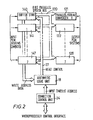
- the device comprises a circuit 10 which receives PCM speech samples on a line 11.
- the circuit 10 has a first output 12 connected to a buffer store 14 and a second output comprising a highway 15 which is also connected to the buffer store 14.
- a further highway 16 links the circuit 10 to an arithmetic logic unit 18.
- the arithmetic logic unit 18 receives local clock signals on a line 20 and a local frame vector on a line 21.
- a connection control unit 24 which is connected by a highway 25 to a microprocessor control unit 30 in the exchange can provide input timeslot address signals to the arithmetic logic unit via highway 26.
- the circuit 10 extracts the remote clock and frame vector signals from the incoming PCM samples on line 11 and generates appropriate write control signals which are fed to the buffer store 14 via highway 15. These signals are used to cyclically write into the buffer store 14 all 32 timeslots which are fed to the store 14 via line 12. The write address for each timeslot is fed to the arithmetic logic unit 18 via highway 16.
- the reading out of information from the store 14 is controlled from the arithmetic logic unit 18 which provides read addresses on a highway 27.
- the arithmetic logic unit 18 operates under the control of the local clock and local frame vector and computes the address in the buffer store 14 of the channel which is to be read out on the basis of data received from the connection control unit 24 and the write address on highway 16 and then enables that channel onto the output highway 28.
- the arithmetic logic unit has to ensure that attempts to simultaneously read and write to the same storage element in the buffer store 14 are avoided. This is achieved in the present arrangement by designing the buffer store 14 so that it is larger than one frame of information such that should a clash be imminent the wanted byte can be taken from an alternative location in the store. This means that slip will have occurred with either the omission of a byte or the repetition of the previous byte. This byte will be read from the same relative location in subsequent frames so that slip does not occur again whilst normal synchronisation is maintained.
- incoming timeslots are read into the buffer store 14 under the control of the remote clock and are read out from that store under the control of the local clock.
- the arrangement thus provides alignment of the incoming data to the local clock and also carries out a time switching function since a particular byte can be read out onto a selected output channel under the control of the arithmetic logic unit 18.
- the arrangement shown in Figure 1 is a single channel aligner and time switch. Similar units can be combined to form an 8 x 8 non-blocking switch by using a common, 8 bit wide, parallel highway containing 256 timeslots operating at 2Mbits/sec. Such an arrangement is shown in Figure 2 of the drawings.
- eight buffer stores 140 to 147 are provided and each buffer store has an 8 bit parallel speech bus 120 which is connected to parallel to serial converters 121 to 128.
- the arrangement of Figure 2 has an arithmetic logic unit 18 which is common to all buffer stores the arithmetic logic unit providing read control signals for the buffer stores onto highway 27.
- the timeslots are ordered such that the parallel to serial output converters 121 to 128 select every eighth byte from the common highway to drive the serial output highways.
- the calculation of the buffer store address can be carried out in 488 n sec (this corresponds to one 2Mbit/sec period).
- the size of the buffer store is critical to the operation of the device.
- the minimum size of the buffer store can be determined by consideration of the aligner function rather than the timeslot interchange function for the following reasons.
- the requirements set out in paragraph 2 above can conveniently be rounded up to seven bytes.
- the requirements set out in paragraphs 1, 2 and 3 then determine that the buffer store should have a minimum size of 43 bytes.
- the mean delay through such a store is 21h bytes or 84 micro seconds.
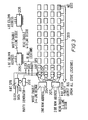
- the buffer store comprises an array of eight bit serial input/parallel output shift registers 200.
- the registers 200 are arranged in four rows of eleven columns the shaded shift register not being used as only 43 bytes of storage are required.
- Clock and data signals are fed to the array of shift registers via an 8 bit serial input parallel output register 201.
- the register 201 also enables a parity generator 202 so that a parity bit is associated with the clock and data signals fed to the registers.
- the decoder 204 receives a two bit row address and decoder 205 receives a four bit column address.
- the two decoders operate together to provide a co-ordinate address for the particular register to which a byte is to be written.
- decoders 207, 208 Similarly reading of the registers is controlled by decoders 207, 208.
- the decoder 207 receives a two bit row address and the decoder 208 receives a four bit column address. These two decoders together provide a co-ordinate address for the particular shift register which is to be enabled for an eight bit byte to be read out onto output bus 209.
- the writing function is carried out under the control of the remote clock whilst the reading function is carried out under the control of the local clock and thus two independent addressing modes are required as shown in Figure 3.
- Timeslot 0 Two mechanisms ensure that all faults in the buffer store are detectable. Firstly, the use of an odd number of shift registers allows timeslot 0 to exercise every storage location. Timeslot . 0 will either contain the frame alignment signal or another pattern if the frame alignment signal has been previously removed. A second fault detection mechanism is provided by the parity bit which is stored with each speech byte and is used to detect what are known as "stuck at" faults on the parallel output from each shift register.
- the data input line is written cyclically into each shift register element in the array under the control of the write enable co-ordinate address provided by the decoders 204 and 205.
- the parallel output from each shift register can be enabled under the control of the read enable co-ordinate address provided by the decoders 207 and 208.
- This read enable co-ordinate address is calculated by the arithmetic logic unit 18 shown in Figures 1 and 2 and is arranged to avoid attempts to read and write simultaneously to the same shift register. The following section describes how this is achieved.
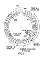
- Figure 4 the forty-three 8-bit stores are shown in a circular array of blocks numbered 0 to 42. It will be appreciated that this is a schematic illustration for ease of understanding and does not represent a physical arrangement. Time can be considered as advancing in a clockwise direction when viewed in Figure 4 and the write address is represented by an arrow 260. The write address moves cyclically in a clockwise direction from one store to the next. Thus, Figure 4 can be considered as a view of the buffer store showing the contents at a particular time.
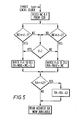
- the F bit which is stored in the connection control unit 24 instructs the arithmetic logic unit 18 as to which formula to use.
- the arithmetic logic unit also calculates a new value of the F bit by comparing RA and WA. To avoid buffer store contention a read operation is not permitted from those stores with addresses WA - 1, WA, WA + 1 and WA + 2.
- a change in the F bit signifies slip that is to say the repetition or omission of a particular byte.
- the size of the buffer store is such that once slip has occurred for a particular byte, no further slip is encountered whilst normal synchronisation is maintained.
Landscapes
- Engineering & Computer Science (AREA)
- Computer Networks & Wireless Communication (AREA)
- Computer Hardware Design (AREA)
- Signal Processing (AREA)
- Time-Division Multiplex Systems (AREA)
- Synchronisation In Digital Transmission Systems (AREA)
- Use Of Switch Circuits For Exchanges And Methods Of Control Of Multiplex Exchanges (AREA)
- Optical Communication System (AREA)
- Communication Control (AREA)
Applications Claiming Priority (2)
| Application Number | Priority Date | Filing Date | Title |
|---|---|---|---|
| GB8224481 | 1982-08-26 | ||
| GB8224481 | 1982-08-26 |
Publications (2)
| Publication Number | Publication Date |
|---|---|
| EP0102810A1 true EP0102810A1 (de) | 1984-03-14 |
| EP0102810B1 EP0102810B1 (de) | 1986-11-26 |
Family
ID=10532528
Family Applications (1)
| Application Number | Title | Priority Date | Filing Date |
|---|---|---|---|
| EP83304891A Expired EP0102810B1 (de) | 1982-08-26 | 1983-08-24 | Digitales Übertragungssystem |
Country Status (15)
| Country | Link |
|---|---|
| US (1) | US4535446A (de) |
| EP (1) | EP0102810B1 (de) |
| JP (1) | JPS5989099A (de) |
| KR (1) | KR840005958A (de) |
| AU (1) | AU558405B2 (de) |
| BR (1) | BR8304595A (de) |
| CA (1) | CA1212743A (de) |
| DE (1) | DE3367994D1 (de) |
| DK (1) | DK390683A (de) |
| ES (1) | ES8405568A1 (de) |
| FI (1) | FI833041A7 (de) |
| NO (1) | NO833046L (de) |
| NZ (1) | NZ205365A (de) |
| PT (1) | PT77252B (de) |
| ZA (1) | ZA836138B (de) |
Cited By (6)
| Publication number | Priority date | Publication date | Assignee | Title |
|---|---|---|---|---|
| EP0255290A3 (en) * | 1986-07-28 | 1988-12-14 | Advanced Micro Devices, Inc. | Time-slot assigner multiplexer |
| EP0210798A3 (en) * | 1985-07-26 | 1988-12-21 | Advanced Micro Devices, Inc. | Programmable data-routing multiplexer |
| EP0323248A3 (en) * | 1987-12-29 | 1990-10-24 | Nec Corporation | Time division switching for multi-channel calls using two time switch memories acting as a frame aligner |
| EP0351779A3 (de) * | 1988-07-18 | 1991-12-18 | Fujitsu Limited | Anordnung zur Phasenregelung eines Taktgebers |
| EP0421934A3 (en) * | 1989-10-06 | 1992-05-13 | Alcatel Str Ag | Method of and arrangement for intelligence transmission between pcm highways |
| US5452305A (en) * | 1993-01-11 | 1995-09-19 | Mitsubishi Denki Kabushiki Kaisha | Frame phase synchronization apparatus and method, and a phase synchronization apparatus of TDM frames |
Families Citing this family (12)
| Publication number | Priority date | Publication date | Assignee | Title |
|---|---|---|---|---|
| GB2151437B (en) * | 1983-12-13 | 1987-04-29 | Plessey Co Plc | Frame aligner for use in telecommunication exchange systems |
| NL8502023A (nl) * | 1985-07-15 | 1987-02-02 | Philips Nv | Werkwijze voor het schakelen van tijdsloten in een tdm-signaal en inrichting voor het uitvoeren van de werkwijze. |
| JPH0666766B2 (ja) * | 1985-10-11 | 1994-08-24 | 日本電気株式会社 | フレ−ムアライナ回路 |
| JPS62188444A (ja) * | 1986-02-13 | 1987-08-18 | Nec Corp | フレ−ム位相同期回路 |
| US5081575A (en) * | 1987-11-06 | 1992-01-14 | Oryx Corporation | Highly parallel computer architecture employing crossbar switch with selectable pipeline delay |
| US5271006A (en) * | 1989-07-19 | 1993-12-14 | Hitachi, Ltd. | Frame aligner and method and system for control thereof |
| JP2804126B2 (ja) * | 1989-11-10 | 1998-09-24 | 株式会社日立製作所 | フレーム位相変換方法および信号伝送方法 |
| JPH0799831B2 (ja) * | 1990-10-08 | 1995-10-25 | 株式会社東芝 | Atm通信システム用単位セルスイッチ |
| US5416778A (en) * | 1992-06-26 | 1995-05-16 | U.S. Philips Corporation | Digital radio communication system and primary and secondary station for use in such a system |
| US5515371A (en) * | 1994-10-26 | 1996-05-07 | Adtran | Timeslot interleaving delay compensation (bonding) mechanism for time division multiplexed digital communication network |
| DE19722433A1 (de) | 1997-05-28 | 1998-12-03 | Siemens Ag | Verfahren und Vorrichtung zur Übertragung eines kontinuierlichen Datenstroms in paketierter Form |
| US6724846B1 (en) | 2000-04-28 | 2004-04-20 | Hewlett-Packard Development Company, L.P. | Simple, high performance, bit-sliced mesochronous synchronizer for a source synchronous link |
Citations (2)
| Publication number | Priority date | Publication date | Assignee | Title |
|---|---|---|---|---|
| CH501344A (de) * | 1969-07-14 | 1970-12-31 | Standard Telephon & Radio Ag | Verfahren zur Durchschaltung von PCM-Kanälen in einer zentralgesteuerten elektronischen Fernmelde-Vermittlungsanlage |
| US3637941A (en) * | 1970-07-13 | 1972-01-25 | Gte Automatic Electric Lab Inc | Integrated switching and transmission network for pulse code modulated signals |
Family Cites Families (5)
| Publication number | Priority date | Publication date | Assignee | Title |
|---|---|---|---|---|
| FR2119152A5 (de) * | 1970-12-22 | 1972-08-04 | Lannionnais Electronique | |
| US3903371A (en) * | 1974-07-01 | 1975-09-02 | Bell Telephone Labor Inc | Common control framing detector |
| JPS5428516A (en) * | 1977-08-08 | 1979-03-03 | Nippon Telegr & Teleph Corp <Ntt> | Channel converter |
| US4224474A (en) * | 1978-09-28 | 1980-09-23 | Western Geophysical Co. Of America | Method and apparatus for demultiplexing multiplexed seismic data |
| US4312063A (en) * | 1979-09-27 | 1982-01-19 | Communications Satellite Corporation | TDM Data reorganization apparatus |
-
1983
- 1983-08-18 AU AU18101/83A patent/AU558405B2/en not_active Ceased
- 1983-08-19 ZA ZA836138A patent/ZA836138B/xx unknown
- 1983-08-19 US US06/524,776 patent/US4535446A/en not_active Expired - Fee Related
- 1983-08-23 NZ NZ205365A patent/NZ205365A/en unknown
- 1983-08-24 ES ES525130A patent/ES8405568A1/es not_active Expired
- 1983-08-24 DE DE8383304891T patent/DE3367994D1/de not_active Expired
- 1983-08-24 NO NO833046A patent/NO833046L/no unknown
- 1983-08-24 CA CA000435218A patent/CA1212743A/en not_active Expired
- 1983-08-24 EP EP83304891A patent/EP0102810B1/de not_active Expired
- 1983-08-25 PT PT77252A patent/PT77252B/pt unknown
- 1983-08-25 BR BR8304595A patent/BR8304595A/pt unknown
- 1983-08-25 FI FI833041A patent/FI833041A7/fi not_active Application Discontinuation
- 1983-08-25 KR KR1019830003977A patent/KR840005958A/ko not_active Withdrawn
- 1983-08-26 DK DK390683A patent/DK390683A/da not_active Application Discontinuation
- 1983-08-26 JP JP58155120A patent/JPS5989099A/ja active Pending
Patent Citations (2)
| Publication number | Priority date | Publication date | Assignee | Title |
|---|---|---|---|---|
| CH501344A (de) * | 1969-07-14 | 1970-12-31 | Standard Telephon & Radio Ag | Verfahren zur Durchschaltung von PCM-Kanälen in einer zentralgesteuerten elektronischen Fernmelde-Vermittlungsanlage |
| US3637941A (en) * | 1970-07-13 | 1972-01-25 | Gte Automatic Electric Lab Inc | Integrated switching and transmission network for pulse code modulated signals |
Non-Patent Citations (4)
| Title |
|---|
| COLLOQUE INTERNATIONAL DE COMMUTATION ELECTRONIQUE, March 28 - April 2, 1966, pages 513-520, Edition Chiron, Paris, FR * |
| ELECTRONICS AND COMMUNICATIONS IN JAPAN, vol. 49, no. 11, November 1966, pages 118-128, IEEE, Washington, US * |
| PROCEEDINGS OF THE IEEE, vol. 65, no. 9, September 1977, pages 1295-1304, New York, US * |
| REVIEW OF ELECTRICAL COMMUNICATION LABORATORIES, vol. 28, nos. 5-6, May-June 1980, pages 328-337, Tokyo, JP * |
Cited By (7)
| Publication number | Priority date | Publication date | Assignee | Title |
|---|---|---|---|---|
| EP0210798A3 (en) * | 1985-07-26 | 1988-12-21 | Advanced Micro Devices, Inc. | Programmable data-routing multiplexer |
| EP0255290A3 (en) * | 1986-07-28 | 1988-12-14 | Advanced Micro Devices, Inc. | Time-slot assigner multiplexer |
| EP0323248A3 (en) * | 1987-12-29 | 1990-10-24 | Nec Corporation | Time division switching for multi-channel calls using two time switch memories acting as a frame aligner |
| EP0351779A3 (de) * | 1988-07-18 | 1991-12-18 | Fujitsu Limited | Anordnung zur Phasenregelung eines Taktgebers |
| EP0421934A3 (en) * | 1989-10-06 | 1992-05-13 | Alcatel Str Ag | Method of and arrangement for intelligence transmission between pcm highways |
| US5452305A (en) * | 1993-01-11 | 1995-09-19 | Mitsubishi Denki Kabushiki Kaisha | Frame phase synchronization apparatus and method, and a phase synchronization apparatus of TDM frames |
| EP0606609A3 (en) * | 1993-01-11 | 1995-09-20 | Mitsubishi Electric Corp | A frame phase synchronization apparatus and method and a phase synchronization apparatus for tdm frames. |
Also Published As
| Publication number | Publication date |
|---|---|
| NO833046L (no) | 1984-02-27 |
| AU1810183A (en) | 1984-03-01 |
| ES525130A0 (es) | 1984-06-16 |
| US4535446A (en) | 1985-08-13 |
| PT77252A (en) | 1983-09-01 |
| ZA836138B (en) | 1984-04-25 |
| DK390683D0 (da) | 1983-08-26 |
| CA1212743A (en) | 1986-10-14 |
| EP0102810B1 (de) | 1986-11-26 |
| AU558405B2 (en) | 1987-01-29 |
| PT77252B (en) | 1986-02-12 |
| FI833041A7 (fi) | 1984-02-27 |
| JPS5989099A (ja) | 1984-05-23 |
| DK390683A (da) | 1984-02-27 |
| ES8405568A1 (es) | 1984-06-16 |
| BR8304595A (pt) | 1984-04-03 |
| NZ205365A (en) | 1986-03-14 |
| DE3367994D1 (en) | 1987-01-15 |
| FI833041A0 (fi) | 1983-08-25 |
| KR840005958A (ko) | 1984-11-19 |
Similar Documents
| Publication | Publication Date | Title |
|---|---|---|
| EP0102810B1 (de) | Digitales Übertragungssystem | |
| EP0323248B1 (de) | Zeitmultiplexvermittlung für Mehrkanal-Verbindungen, welche zwei Zeitvermittlungsspeicher als Rahmenausgleicher verwendet | |
| US5119368A (en) | High-speed time-division switching system | |
| US4392234A (en) | PCM Signal interface apparatus | |
| US6259703B1 (en) | Time slot assigner for communication system | |
| US4686670A (en) | Method of switching time slots in a TDM-signal and arrangement for performing the method | |
| US4967410A (en) | Method of multiplexing digital signals and apparatus therefor | |
| US4894821A (en) | Time division switching system with time slot alignment circuitry | |
| US5796733A (en) | Time division switching system | |
| US5305322A (en) | Phase alignment circuit for stuffed-synchronized TDM transmission system with cross-connect function | |
| JPH05191441A (ja) | 非同期時分割データパケットと同様に同期時分割信号を処理するためのシステム | |
| US4086437A (en) | Resynchronizing circuit for TDM system | |
| US4060698A (en) | Digital switching center | |
| FI73346C (fi) | Anordning foer att synkronisera multiplexrar vid en digitalstation. | |
| GB2066627A (en) | P.C.M. frame aligner with frame slip characteristic | |
| JPH01176197A (ja) | 時分割多元交換方式 | |
| CA2109007C (en) | Time slot assigner for communication system | |
| RU2012153C1 (ru) | Цифровое коммутационное поле | |
| JP3082577B2 (ja) | 先入先出メモリ装置 | |
| JP3199418B2 (ja) | データレート変換装置 | |
| KR0183135B1 (ko) | 동기램과 비동기램을 이용한 시간 스위칭 장치 | |
| SU1667087A1 (ru) | Устройство дл управлени обменом процессора с пам тью | |
| SU1019636A1 (ru) | Мажоритарное устройство | |
| KR0168921B1 (ko) | 동기식 전송시스템에서 시험액세스를 위한 24x3교차 스위치 회로 | |
| SU866774A1 (ru) | Устройство дл коммутации телеграфных каналов |
Legal Events
| Date | Code | Title | Description |
|---|---|---|---|
| PUAI | Public reference made under article 153(3) epc to a published international application that has entered the european phase |
Free format text: ORIGINAL CODE: 0009012 |
|
| AK | Designated contracting states |
Designated state(s): BE CH DE FR GB IT LI NL SE |
|
| 17P | Request for examination filed |
Effective date: 19840806 |
|
| GRAA | (expected) grant |
Free format text: ORIGINAL CODE: 0009210 |
|
| AK | Designated contracting states |
Kind code of ref document: B1 Designated state(s): BE CH DE FR GB IT LI NL SE |
|
| ITF | It: translation for a ep patent filed | ||
| REF | Corresponds to: |
Ref document number: 3367994 Country of ref document: DE Date of ref document: 19870115 |
|
| RAP2 | Party data changed (patent owner data changed or rights of a patent transferred) |
Owner name: BRITISH TELECOMMUNICATIONS |
|
| ET | Fr: translation filed | ||
| REG | Reference to a national code |
Ref country code: GB Ref legal event code: 732 |
|
| PG25 | Lapsed in a contracting state [announced via postgrant information from national office to epo] |
Ref country code: SE Effective date: 19870825 |
|
| PG25 | Lapsed in a contracting state [announced via postgrant information from national office to epo] |
Ref country code: LI Effective date: 19870831 Ref country code: CH Effective date: 19870831 |
|
| PLBE | No opposition filed within time limit |
Free format text: ORIGINAL CODE: 0009261 |
|
| STAA | Information on the status of an ep patent application or granted ep patent |
Free format text: STATUS: NO OPPOSITION FILED WITHIN TIME LIMIT |
|
| 26N | No opposition filed | ||
| BERE | Be: lapsed |
Owner name: BRITISH TELECOMMUNICATIONS Effective date: 19870831 |
|
| PG25 | Lapsed in a contracting state [announced via postgrant information from national office to epo] |
Ref country code: NL Effective date: 19880301 |
|
| NLV4 | Nl: lapsed or anulled due to non-payment of the annual fee | ||
| PG25 | Lapsed in a contracting state [announced via postgrant information from national office to epo] |
Ref country code: FR Free format text: LAPSE BECAUSE OF NON-PAYMENT OF DUE FEES Effective date: 19880429 |
|
| REG | Reference to a national code |
Ref country code: CH Ref legal event code: PL |
|
| PG25 | Lapsed in a contracting state [announced via postgrant information from national office to epo] |
Ref country code: DE Effective date: 19880503 |
|
| GBPC | Gb: european patent ceased through non-payment of renewal fee | ||
| REG | Reference to a national code |
Ref country code: FR Ref legal event code: ST |
|
| PG25 | Lapsed in a contracting state [announced via postgrant information from national office to epo] |
Ref country code: GB Free format text: LAPSE BECAUSE OF NON-PAYMENT OF DUE FEES Effective date: 19881122 |
|
| PG25 | Lapsed in a contracting state [announced via postgrant information from national office to epo] |
Ref country code: BE Effective date: 19890831 |
|
| EUG | Se: european patent has lapsed |
Ref document number: 83304891.1 Effective date: 19880711 |