EP0105711A2 - Détermination de la position d'un substrat à l'aide de faisceaux d'électrons - Google Patents
Détermination de la position d'un substrat à l'aide de faisceaux d'électrons Download PDFInfo
- Publication number
- EP0105711A2 EP0105711A2 EP83305829A EP83305829A EP0105711A2 EP 0105711 A2 EP0105711 A2 EP 0105711A2 EP 83305829 A EP83305829 A EP 83305829A EP 83305829 A EP83305829 A EP 83305829A EP 0105711 A2 EP0105711 A2 EP 0105711A2
- Authority
- EP
- European Patent Office
- Prior art keywords
- wafer
- mark
- determining
- marks
- line groups
- Prior art date
- Legal status (The legal status is an assumption and is not a legal conclusion. Google has not performed a legal analysis and makes no representation as to the accuracy of the status listed.)
- Granted
Links
Images


Classifications
-
- H—ELECTRICITY
- H01—ELECTRIC ELEMENTS
- H01J—ELECTRIC DISCHARGE TUBES OR DISCHARGE LAMPS
- H01J37/00—Discharge tubes with provision for introducing objects or material to be exposed to the discharge, e.g. for the purpose of examination or processing thereof
- H01J37/30—Electron-beam or ion-beam tubes for localised treatment of objects
- H01J37/304—Controlling tubes by information coming from the objects or from the beam, e.g. correction signals
- H01J37/3045—Object or beam position registration
Definitions
- the present invention relates to a method for determining the position of a wafer by means of electron beams and to a wafer having chips for determining the position of the wafer. More particularly, it relates to a method and a chip for determining the position of a wafer in which the chip is given a specific pattern so as to enable accurate determination of the position of the wafer with respect to the electron beams with a small scan width.
- the wafer when forming a pattern on a wafer using an electron beam exposure apparatus, the wafer must be positioned to the pattern-forming electron beam with an accuracy of about 0.1 ⁇ m.
- a chip with a large mark mounted on a wafer and is at first scanned in a rough adjusting step by an electron beam of secondary electrons, reflected electrons, and so forth, to determine the position of the wafer with an accuracy of about 1 ⁇ m. Then, a chip with a small mark mounted on the wafer is scanned in a fine adjusting step, to determine the position of the wafer with an accuracy of 0.1 ⁇ m.
- the large mark in the rough adjusting chip has a relatively simple shape, it is difficult to distinguish it from dust on the wafer or patterns on other semiconductor chips.
- An embodiment of the present invention can provide a method and a wafer with chips for determining the position of the wafer in which other chips are not destroyed and the same position-determining chip can be scanned a number of times.
- An embodiment of the present invention can also provide the above method and wafer in which a relatively small position-determining chip in comparison with the conventional position-determining chip can be used, thus enabling effective use of the wafer for semiconductor chips.
- An embodiment of of the present invention can to provide the above method and wafer in which marks on the position-determining chip can easily be distinguished from dust on the wafer or other patterns on the other semiconductor chips.
- a method for determining the position of a wafer comprising the steps of scanning, by means of an electron beam, one of a plurality of first-direction (Y-direction) line groups formed on a region of at least one position--determining chip on the wafer and extending in parallel from each other, each of the first-direction line groups comprising one first-direction main mark and one first--direction code mark expressing the position of the one first-direction main mark; and scanning, by means of an electron beam, one of a plurality of second-direction (X-direction) line groups formed on one side of the at least one position-determining chip on the wafer and extending in the direction orthogonal to the extending direction of the first-direction line groups, each of the second-direction line groups comprising one second--direction main mark and one second-direction code mark expressing the position of the one second-direction main mark.
- Y-direction first-direction
- An embodiment of the present invention may further include the steps of: analyzing the scanned first-direction code mark after scanning said.one first-direction line group so as to determine the position of the scanned first -direction main mark, and analyzing the scanned second-direction code mark after scanning said one second-direction line group so as to determine the position of the scanned second-direction main mark.
- a wafer having position-determining chips for determining the position of said wafer by means of electron beams, at least one of said position determining chips comprising: a plurality of first--direction (X-direction) line groups formed on one side portion of said at least one position-determining chip and extending in parallel from each other; a plurality of second-direction (Y-direction) line groups formed on the other region of said at least one position--determining chips and extending in the direction orthogonal to the extending direction of said first--direction line groups, said second-direction line groups extending in parallel from each other; each of said first-direction line groups comprising one first--direction main mark and one first-direction code mark expressing the position of said one first-direction main mark; each of said second-direction line groups comprising one second-direction main mark and one second-direction code mark expressing the position of said one second-direction main mark; whereby, by scanning one of said first-direction
- Said first-direction main marks may be separated from each other by a predetermined distance, and said second-direction main marks may be separated from each other by said predetermined distance.
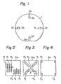
- the wafer 1 Before the rough adjusting process, the wafer 1 is positioned on a work table with an accuracy of 2 mm through 5 mm. Therefore, the rough adjusting chips in Figs. 1 through 3 should have a side length of at least 5 mm.
- the length of the scan line should be at least 5 mm.
- the distance between the position-determining chip and a semiconductor chip (not shown in Fig. 1) is less than 5 mm. Accordingly, as mentioned earlier, there is the problem that, in the rough adjusting process, a scan line may erroneously cover and thus destroy a semiconductor chip (not shown) adjacent to a rough adjusting chip.
- Figure 5 is a plan view of an example of a conventional rough adjusting chip having a plurality of marks.
- a number of marks M 1 , M 2 , M 3 , --- are formed on one chip 2a3.
- the chip 2a3 has a large area, thus limiting the effective area for semiconductor chips on the wafer.
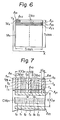
- Figure 6 is a general plan view of a chip for determining the position of a wafer according to an embodiment of the present invention.
- a position-determining chip 2a O is a square having a side length of 5 mm, for example.
- an X-direction mark M X is formed for roughly adjusting the position of the wafer in the X direction.
- the X-direction mark M X has a plurality of X-direction main marks l X1 , l X2 , --- arranged in parallel in the X direction at equal intervals therebetween.
- Each of the X-direction main marks l X1 , l X2 , --- extends in the Y direction and has, for example, a length of 500 ⁇ m.
- the interval between adjacent X-direction main marks is, for example, 100 ⁇ m. Therefore, in this case, 50 main marks are formed on the position-determining chip 2a.
- a Y-direction mark My for roughly adjusting the position of the wafer in the Y direction.
- the Y-direction mark My has a plurality of Y-direction main marks l y1 , l y2 , l y3 , --- arranged in parallel in the Y direction at equal intervals.
- Each of the Y-direction main marks l y1 , l y2 , l y3 , --- extends in the X direction and has the same length as the side length of the position determining chip 2a 0 .
- the interval between adjacent Y-direction main marks is also, for example, 100 ⁇ m.
- FIG. 7 is an expanded plan view of a part of Fig. 6.
- each of the X-direction main marks l x1 , l x2 , l x3 , --- has a width of 16 ⁇ m.
- Each of the Y-direction main marks l y1 , l y2 , --- has the same width of 16 ⁇ m.
- an X-direc- tion code mark CM xi for roughly determining the position of the X-direction main marks is formed.
- a Y-direction code mark CM for roughly determining the position of the Y-direction main marks is formed.
- Each X-direction code mark CM xi has up to six fine lines f o to f 5 for expressing a position code of the adjacent main mark l xi .
- CM xl has no fine lines
- CM x2 has one fine line f 0 .
- solid lines are used to indicate actual fine lines. The dash lines in the figure indicate merely the possible positions of other fine lines and are provided only for ease of understanding.
- the fine line f 0 in the X-direction code mark CM x2 thus expresses "1", while the empty positions of the fine lines f 1 to f 5 in the code mark CM x2 express "0"s.
- Each Y-direction code mark CM also has up to six fine lines f 0 to f 5 so as to express a position code of the adjacent main mark l Yi .
- Figure 8 is an expanded cross-sectional view taken along line VII-VII of Fig. 7.
- the X-direction code mark CM xl actually has no fine line. If a fine line did exist, it would have a width of for example, 4 m
- the X-direction main marks l xl , l x2 , --- and the code marks CM xi can be formed as grooves on the wafer 1.
- the X-direction main mark l xl and its adjacent X-direction code mark CM xl constitute a line group lG xl .
- an X-direction main mark l xi and its adjacent X-direction code mark CM xi constitute a line group lG xi .
- the position--determining chip 2a 0 is scanned in the Y direction by an electron beam with a scan length of 100 ⁇ m so as to scan one of the Y-direction main marks l y1 , l y2 , Because the scan length and the interval between adjacent main marks are only 100 um, respectively, the electron beam does not scan and destroy any semiconductor chip adjacent to the position-determining chip 2a 0 .
- the work table is moved in the Y direction by 50 ⁇ m. The process is repeated until a Y-direction main mark is found.
- the Y-direction code mark in the line group including the found Y-direction main mark is read so as to determine the position of the scanned Y-direction main mark.
- the scanned Y-direction main mark can be identified among a number of Y-direction main marks.
- the Y-direction position of the wafer is determined with an accuracy of 100 ⁇ m.
- the work table is then moved in the Y direction so that the electron beam can scan the region of the X- direction mark M x . to be moved
- the distanced between the position of the found Y-direction main mark and the region of the X-direction mark M x is found by simple calculation.
- the position-determining chip 2A O is scanned in the X direction by an electron beam with a scan length of 100 pm so as to scan one of the X-direction main marks l x1 , l x2 , ---.
- the work table is moved in the X-direction by 50 ⁇ m. The process is repeated until an X-direction main mark is found.
- the X direction code mark in the line group including the found X-direction main mark is read to determine the position of the scanned X-direction main mark with an accuracy of 100 ⁇ m.
- the scanned X-direction main mark can be identified among a number of X-direction main marks.
- the position of the wafer can be determined with an accuracy of 100 ⁇ m.
- the central position between the scanned X-direction main mark and its adjacent X-direction main mark and the central position between the scanned Y-direction main mark and its adjacent Y-direction main mark can be determined with an accuracy of 0.1 ⁇ m in a conventional way, for example, by determining the edges of the scanned main marks and their adjacent main marks.
- Figure 9 is a general plan view of a position-determining chip according to another embodiment of the present invention. The difference between Fig. 6 and Fig. 9 is that, in Fig. 9, the position-determining
- chip 2a 0 has, on its periphery, projected patterns P1 to P 4 for detecting the angle of the wafer rotation.
- the inclination of the wafer with respect to the X direction can be determined.
- the pattern P 2 and P 9 the inclination of the wafer with respect to the Y direction can be determined.
- the present invention is not restricted to the above-described embodiments. Various changes and modifications are possible without departing from the spirit of the present invention. For example, the position and the size of the region for the X-direction main marks or the Y-direction main marks may be changed. Also, the number of the main marks may be changed. Each code mark may have any number of fine lines. Further, instead of forming grooves for the main marks and the code marks on the wafer, these marks may be formed by a projections on the wafer or by/different material such as silicon dioxide, aluminum, polycrystalline silicon, phosphosilicate glass, and silicon nitride, on the silicon wafer.
- the position of the wafer can be determined without destroying other chips as the position-determining chip can be scanned with a short scanning line in comparison with the prior art.
- the marks on the position--determining chip can easily be distinguished from dust on the wafer or other patterns on the other semiconductor chips.
- the position-determining chip can withstand a number of scans by electron beams.
- position-determining chip is small in comparison with conventional position- -determining chips including a number of marks, a greater area of the wafer can be used for semiconductor chips.
- the present invention is not only applicableto an electron beam exposure apparatus, but also to a wafer inspecting apparatus using electron beams or to a size-length measuring apparatus using electron beams.
Landscapes
- Chemical & Material Sciences (AREA)
- Analytical Chemistry (AREA)
- Electron Beam Exposure (AREA)
- Length-Measuring Devices Using Wave Or Particle Radiation (AREA)
- Exposure And Positioning Against Photoresist Photosensitive Materials (AREA)
- Container, Conveyance, Adherence, Positioning, Of Wafer (AREA)
Applications Claiming Priority (2)
| Application Number | Priority Date | Filing Date | Title |
|---|---|---|---|
| JP172170/82 | 1982-09-30 | ||
| JP57172170A JPS5960306A (ja) | 1982-09-30 | 1982-09-30 | 位置決定用チップを備えた試料 |
Publications (3)
| Publication Number | Publication Date |
|---|---|
| EP0105711A2 true EP0105711A2 (fr) | 1984-04-18 |
| EP0105711A3 EP0105711A3 (en) | 1986-02-19 |
| EP0105711B1 EP0105711B1 (fr) | 1989-07-19 |
Family
ID=15936865
Family Applications (1)
| Application Number | Title | Priority Date | Filing Date |
|---|---|---|---|
| EP83305829A Expired EP0105711B1 (fr) | 1982-09-30 | 1983-09-28 | Détermination de la position d'un substrat à l'aide de faisceaux d'électrons |
Country Status (4)
| Country | Link |
|---|---|
| US (1) | US4564764A (fr) |
| EP (1) | EP0105711B1 (fr) |
| JP (1) | JPS5960306A (fr) |
| DE (1) | DE3380230D1 (fr) |
Cited By (3)
| Publication number | Priority date | Publication date | Assignee | Title |
|---|---|---|---|---|
| EP0226893A1 (fr) * | 1985-12-13 | 1987-07-01 | Siemens Aktiengesellschaft | Procédé de haute précision de mesure pour structures bidimensionnelles ainsi que masque de référence pour l'utilisation de ce procédé |
| FR2709868A1 (fr) * | 1994-08-23 | 1995-03-17 | Schlumberger Technologies Inc | Grille de positionnement pour gravure par faisceau ionique focalisé. |
| US5438207A (en) * | 1993-11-17 | 1995-08-01 | Nec Corporation | Electron beam direct writing system for ULSI lithography with facilitated rotation and gain corrections of shot patterns and electron beam direct writing method for same |
Families Citing this family (6)
| Publication number | Priority date | Publication date | Assignee | Title |
|---|---|---|---|---|
| JP2723508B2 (ja) * | 1985-10-21 | 1998-03-09 | 日本電気株式会社 | 電子線直接描画のためのアライメント方法 |
| JPS62208627A (ja) * | 1986-03-07 | 1987-09-12 | Jeol Ltd | 荷電粒子線描画におけるマ−ク位置検出方法 |
| JPH07111954B2 (ja) * | 1989-03-15 | 1995-11-29 | 光計測技術開発株式会社 | 電子ビーム露光装置 |
| US5087537A (en) * | 1989-10-11 | 1992-02-11 | International Business Machines Corporation | Lithography imaging tool and related photolithographic processes |
| EP0669636A1 (fr) * | 1994-02-25 | 1995-08-30 | AT&T Corp. | Détection d'erreur dans un système de fabrication |
| US6126382A (en) * | 1997-11-26 | 2000-10-03 | Novellus Systems, Inc. | Apparatus for aligning substrate to chuck in processing chamber |
Family Cites Families (8)
| Publication number | Priority date | Publication date | Assignee | Title |
|---|---|---|---|---|
| BE756684A (fr) * | 1969-09-25 | 1971-03-01 | Commw Of Australia | Dispositif pour le routage de signaux de telecommunication discontinus |
| US3603974A (en) * | 1969-12-31 | 1971-09-07 | Nasa | High speed photo-optical time recording |
| GB1328976A (en) * | 1970-12-22 | 1973-09-05 | Marconi Co Ltd | Electronic scanning devices |
| US3849659A (en) * | 1973-09-10 | 1974-11-19 | Westinghouse Electric Corp | Alignment of a patterned electron beam with a member by electron backscatter |
| GB1520925A (en) * | 1975-10-06 | 1978-08-09 | Mullard Ltd | Semiconductor device manufacture |
| US4327292A (en) * | 1980-05-13 | 1982-04-27 | Hughes Aircraft Company | Alignment process using serial detection of repetitively patterned alignment marks |
| JPS5795627A (en) * | 1980-12-05 | 1982-06-14 | Nippon Telegr & Teleph Corp <Ntt> | Method for arranging mark in electron beam exposure |
| JPS57210628A (en) * | 1981-06-19 | 1982-12-24 | Hitachi Ltd | Retrieving method for pattern data in electron beam drawing device |
-
1982
- 1982-09-30 JP JP57172170A patent/JPS5960306A/ja active Granted
-
1983
- 1983-09-28 EP EP83305829A patent/EP0105711B1/fr not_active Expired
- 1983-09-28 DE DE8383305829T patent/DE3380230D1/de not_active Expired
- 1983-09-30 US US06/537,624 patent/US4564764A/en not_active Expired - Lifetime
Cited By (3)
| Publication number | Priority date | Publication date | Assignee | Title |
|---|---|---|---|---|
| EP0226893A1 (fr) * | 1985-12-13 | 1987-07-01 | Siemens Aktiengesellschaft | Procédé de haute précision de mesure pour structures bidimensionnelles ainsi que masque de référence pour l'utilisation de ce procédé |
| US5438207A (en) * | 1993-11-17 | 1995-08-01 | Nec Corporation | Electron beam direct writing system for ULSI lithography with facilitated rotation and gain corrections of shot patterns and electron beam direct writing method for same |
| FR2709868A1 (fr) * | 1994-08-23 | 1995-03-17 | Schlumberger Technologies Inc | Grille de positionnement pour gravure par faisceau ionique focalisé. |
Also Published As
| Publication number | Publication date |
|---|---|
| EP0105711B1 (fr) | 1989-07-19 |
| DE3380230D1 (en) | 1989-08-24 |
| EP0105711A3 (en) | 1986-02-19 |
| US4564764A (en) | 1986-01-14 |
| JPS6352328B2 (fr) | 1988-10-18 |
| JPS5960306A (ja) | 1984-04-06 |
Similar Documents
| Publication | Publication Date | Title |
|---|---|---|
| KR100310497B1 (ko) | 독특하게위치된얼라인먼트마크를사용하는전자빔리소그래피방법과그얼라인먼트마크를구비하는웨이퍼 | |
| US5777392A (en) | Semiconductor device having improved alignment marks | |
| US4585931A (en) | Method for automatically identifying semiconductor wafers | |
| EP0105711A2 (fr) | Détermination de la position d'un substrat à l'aide de faisceaux d'électrons | |
| EP0130819B1 (fr) | Procédé pour le positionnement d'un faisceau à une partie spécifique d'une pastille semi-conductrice | |
| US5552611A (en) | Pseudo-random registration masks for projection lithography tool | |
| US7007855B1 (en) | Wafer identification mark | |
| US6218199B1 (en) | Silicon substrate with identification data | |
| JP2723508B2 (ja) | 電子線直接描画のためのアライメント方法 | |
| GB2109538A (en) | Electron beam alignment | |
| KR100217445B1 (ko) | 정렬 마크를 가진 반도체 장치 | |
| US4932064A (en) | Semiconductor device | |
| US4808829A (en) | Mark position detection system for use in charged particle beam apparatus | |
| US6666337B1 (en) | Method and apparatus for determining wafer identity and orientation | |
| EP0078578B1 (fr) | Méthode d'utilisation d'un faisceau d'électrons | |
| JPH0713997B2 (ja) | ウエハの要位置合せ角検出装置 | |
| US6468704B1 (en) | Method for improved photomask alignment after epitaxial process through 90° orientation change | |
| JPS63168708A (ja) | 回転位置決め装置 | |
| US12055859B2 (en) | Overlay mark design for electron beam overlay | |
| JPH11340131A (ja) | 半導体集積回路の製造方法 | |
| JPH11175737A (ja) | ハニカム構造体の位置決め方法および加工方法 | |
| JPS6222010A (ja) | パタ−ン欠陥検出方法 | |
| GB2328761A (en) | Mask preparation method including critical dimension test forming means | |
| KR20010028937A (ko) | 반도체 웨이퍼 패턴의 크기 및 오버레이 측정방법 | |
| JPS6234135B2 (fr) |
Legal Events
| Date | Code | Title | Description |
|---|---|---|---|
| PUAI | Public reference made under article 153(3) epc to a published international application that has entered the european phase |
Free format text: ORIGINAL CODE: 0009012 |
|
| AK | Designated contracting states |
Designated state(s): DE FR GB |
|
| PUAL | Search report despatched |
Free format text: ORIGINAL CODE: 0009013 |
|
| AK | Designated contracting states |
Designated state(s): DE FR GB |
|
| 17P | Request for examination filed |
Effective date: 19860804 |
|
| 17Q | First examination report despatched |
Effective date: 19871120 |
|
| GRAA | (expected) grant |
Free format text: ORIGINAL CODE: 0009210 |
|
| AK | Designated contracting states |
Kind code of ref document: B1 Designated state(s): DE FR GB |
|
| REF | Corresponds to: |
Ref document number: 3380230 Country of ref document: DE Date of ref document: 19890824 |
|
| ET | Fr: translation filed | ||
| PLBE | No opposition filed within time limit |
Free format text: ORIGINAL CODE: 0009261 |
|
| STAA | Information on the status of an ep patent application or granted ep patent |
Free format text: STATUS: NO OPPOSITION FILED WITHIN TIME LIMIT |
|
| 26N | No opposition filed | ||
| PGFP | Annual fee paid to national office [announced via postgrant information from national office to epo] |
Ref country code: GB Payment date: 19990922 Year of fee payment: 17 |
|
| PG25 | Lapsed in a contracting state [announced via postgrant information from national office to epo] |
Ref country code: GB Free format text: LAPSE BECAUSE OF NON-PAYMENT OF DUE FEES Effective date: 20000928 |
|
| GBPC | Gb: european patent ceased through non-payment of renewal fee |
Effective date: 20000928 |
|
| PGFP | Annual fee paid to national office [announced via postgrant information from national office to epo] |
Ref country code: FR Payment date: 20010911 Year of fee payment: 19 |
|
| PGFP | Annual fee paid to national office [announced via postgrant information from national office to epo] |
Ref country code: DE Payment date: 20011015 Year of fee payment: 19 |
|
| PG25 | Lapsed in a contracting state [announced via postgrant information from national office to epo] |
Ref country code: DE Free format text: LAPSE BECAUSE OF NON-PAYMENT OF DUE FEES Effective date: 20030401 |
|
| PG25 | Lapsed in a contracting state [announced via postgrant information from national office to epo] |
Ref country code: FR Free format text: LAPSE BECAUSE OF NON-PAYMENT OF DUE FEES Effective date: 20030603 |
|
| REG | Reference to a national code |
Ref country code: FR Ref legal event code: ST |