EP0110465A2 - Chinoxalin-Polymere mit Biphenylen-Endgruppen und ihre Verwendung als Isolierüberzüge in Halbleiterelementen - Google Patents
Chinoxalin-Polymere mit Biphenylen-Endgruppen und ihre Verwendung als Isolierüberzüge in Halbleiterelementen Download PDFInfo
- Publication number
- EP0110465A2 EP0110465A2 EP83201633A EP83201633A EP0110465A2 EP 0110465 A2 EP0110465 A2 EP 0110465A2 EP 83201633 A EP83201633 A EP 83201633A EP 83201633 A EP83201633 A EP 83201633A EP 0110465 A2 EP0110465 A2 EP 0110465A2
- Authority
- EP
- European Patent Office
- Prior art keywords
- biphenylene
- quinoxaline
- capped
- prepolymer
- benzocyclobutadienoquinone
- Prior art date
- Legal status (The legal status is an assumption and is not a legal conclusion. Google has not performed a legal analysis and makes no representation as to the accuracy of the status listed.)
- Granted
Links
Images
Classifications
-
- H—ELECTRICITY
- H10—SEMICONDUCTOR DEVICES; ELECTRIC SOLID-STATE DEVICES NOT OTHERWISE PROVIDED FOR
- H10P—GENERIC PROCESSES OR APPARATUS FOR THE MANUFACTURE OR TREATMENT OF DEVICES COVERED BY CLASS H10
- H10P14/00—Formation of materials, e.g. in the shape of layers or pillars
- H10P14/60—Formation of materials, e.g. in the shape of layers or pillars of insulating materials
- H10P14/68—Organic materials, e.g. photoresists
- H10P14/683—Organic materials, e.g. photoresists carbon-based polymeric organic materials, e.g. polyimides, poly cyclobutene or PVC
-
- C—CHEMISTRY; METALLURGY
- C08—ORGANIC MACROMOLECULAR COMPOUNDS; THEIR PREPARATION OR CHEMICAL WORKING-UP; COMPOSITIONS BASED THEREON
- C08G—MACROMOLECULAR COMPOUNDS OBTAINED OTHERWISE THAN BY REACTIONS ONLY INVOLVING UNSATURATED CARBON-TO-CARBON BONDS
- C08G73/00—Macromolecular compounds obtained by reactions forming a linkage containing nitrogen with or without oxygen or carbon in the main chain of the macromolecule, not provided for in groups C08G12/00 - C08G71/00
- C08G73/06—Polycondensates having nitrogen-containing heterocyclic rings in the main chain of the macromolecule
- C08G73/0683—Polycondensates containing six-membered rings, condensed with other rings, with nitrogen atoms as the only ring hetero atoms
- C08G73/0694—Polycondensates containing six-membered rings, condensed with other rings, with nitrogen atoms as the only ring hetero atoms with only two nitrogen atoms in the ring, e.g. polyquinoxalines
-
- H—ELECTRICITY
- H01—ELECTRIC ELEMENTS
- H01B—CABLES; CONDUCTORS; INSULATORS; SELECTION OF MATERIALS FOR THEIR CONDUCTIVE, INSULATING OR DIELECTRIC PROPERTIES
- H01B3/00—Insulators or insulating bodies characterised by the insulating materials; Selection of materials for their insulating or dielectric properties
- H01B3/18—Insulators or insulating bodies characterised by the insulating materials; Selection of materials for their insulating or dielectric properties mainly consisting of organic substances
- H01B3/30—Insulators or insulating bodies characterised by the insulating materials; Selection of materials for their insulating or dielectric properties mainly consisting of organic substances plastics; resins; waxes
- H01B3/303—Macromolecular compounds obtained by reactions forming a linkage containing nitrogen with or without oxygen or carbon in the main chain of the macromolecule, not provided for in groups H01B3/38 or H01B3/302
-
- H—ELECTRICITY
- H10—SEMICONDUCTOR DEVICES; ELECTRIC SOLID-STATE DEVICES NOT OTHERWISE PROVIDED FOR
- H10P—GENERIC PROCESSES OR APPARATUS FOR THE MANUFACTURE OR TREATMENT OF DEVICES COVERED BY CLASS H10
- H10P14/00—Formation of materials, e.g. in the shape of layers or pillars
- H10P14/60—Formation of materials, e.g. in the shape of layers or pillars of insulating materials
- H10P14/63—Formation of materials, e.g. in the shape of layers or pillars of insulating materials characterised by the formation processes
- H10P14/6326—Deposition processes
- H10P14/6342—Liquid deposition, e.g. spin-coating, sol-gel techniques or spray coating
Definitions
- This invention relates to insulating or masking coatings for semiconductor devices, and more in particular to forming such coatings from cured compositions of biphenylene end-capped quinoxaline prepolymers.
- One object of this invention is to provide improved insulating and masking coatings for electronic components as for example, semiconductor component structures.
- Another object of this invention is to provide new insulating and masking coatings for use on semiconductor components.
- Another object of this invention is to provide an improved prepolymer of a biphenylene end-capped quinoxaline which can be used as insulating or masking coatings on electronic components, such as semiconductor integrated circuits.
- Another object of the present invention is to provide cured biphenylene end-capped prepolymers on semiconductor structures such as integrated circuit devices and/or substrate carriers therefor.
- Another object of the present invention is to provide cross-linked polymers of biphenylene end-capped quinoxaline compositions as coatings on semiconductor components.
- Another object of the present invention is to provide biphenylene end-capped quinoxaline compositions which can be cured by addition reactions into cross-linked polymers.
- Another object of the present invention is to provide a method for forming biphenylene end-capped quinoxaline compositions.
- Another object of the present invention is to provide cross-linked polymers of biphenylene end-capped quinoxalines.
- polymeric resins in the fabrication of electronic components such as semiconductor integrated circuits and/or supporting carriers therefor.
- polymeric compositions include the polyimides, such as described in U.S. Patents No. 3,684,592 and No. 3,700,497, whose properties have made them attractive for semiconductor devices or integrated circuits.
- These polyimides are condensation products of pyromellitic dianhydride and an aromatic diamine, possessing properties which made them attractive for passivation of semiconductor devices, encapsulation thereof against contaminants in the ambient, and as masks for deposition of metallization in an interconnecting pattern between elements of an integrated circuit device.
- these polyimide polymers are cross-linked, on curing by condensation reactions, the process is accompanied by the evolution of volatiles which tend to form voids in the cured product which detracts from their suitability in said applications.
- the substituted biphenylene (III) was then modified in various ways and subsequently incorporated in a polymer chain. Typical of the polymer chains are the quinoxaline polymers. However, the use of biphenylene poses a problem since it is difficult and dangerous to make.
- curable quinoxaline polymers or prepolymers are those discussed in U.S. Patents No. 3,852,243 and No. 4,125,725.
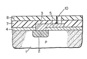
- Fig. 1 is a fragmentary view in elevation of a semiconductor device for purposes of illustrating this invention.
- the biphenylene group can be incorporated in a polymer (e.g. quinoxaline) by end-capping the polymer with a 1,2-diketone (IV).
- a polymer e.g. quinoxaline
- IV 1,2-diketone
- the diketone can then be reacted with orthodiamines (for example, constituent of quinoxalines) to give end-capped structures (V) as follows
- a specific application of this invention is in the use of benzocyclobutadienoquinone (IV) to prepare quinoxaline prepolymers containing the biphenylene terminal unit. These biphenylene units are incorporated at the ends of the chain. Previous quinoxaline polymers have had this biphenylene unit incorporated within the chain, see A. Recca et al noted above, where such synthesis involved the formation of biphenylene (I) which was then converted to the 2,6-diglyoxalyldiphenylene dihydrate (VI): prior to the formation of the quinoxaline polymers.
- the resultant end-capped polymer composition can be represented by the following structural formulas. where R can be a direct bond, -0-, -S- or to 20. and n is an integer from 1
- Structures (VIII) and (X) incorporate both biphenylene and acetylene curing sites, thus providing a two step curing process.
- Such a cure offers advantages in certain applications requiring multi-layer coatings of a cured product, where each applied layer of the prepolymer (e.g. structures (VIII) and (X)) need to be partially cured before subsequent layers are deposited. This was evidenced in DCS traces for structure (X) which showed exotherms at about 300°C and at about 425°C, which can be attributed to the acetylene and biphenylene groups, respectively.
- the biphenylene end-capped polymers are soluble in suitable solvents, such as N-methylpyrrolidone, and can be spun coated on substrates (e.g. semiconductor wafers) in conventional manner.
- suitable solvents such as N-methylpyrrolidone
- the cured polymers also have good thermal stability by virtue of their aromatic structure, where for example, structure (X) showed only a 4X weight loss on heating to 500°C in nitrogen.
- Benzocyclobutadienoquinone (IV) was prepared as indicated below in accordance with published procedures as described by Cava et al noted above; Cava and Napier, J. Am. Chem. Soc., 79, 1701 (1957); Jensen and Coleman, J. Org. Chem., 23, 869 (1958); and Schmidt and Ried, Synthesis, 869 (1978):
- the diketone (IV) was purified by recrystallization from methylenechloride/ hexane solution followed by sublimation under vacuum at 100°C.
- the mixture was brought to reflux for an hour.
- the product was isolated by pouring the tetrahydrofuran solution into 100 mls. MeOH (methanol). The product was filtered, washed three times with MeOH, and dried under vacuum. The yield was better than 80%.
- n is an integer from 1 to 20.
- oligomers are prepared in accordance with the reaction: Using a similar procedure as described in Example 4, an oligomer (X) was prepared with 0.82 grams (0.0038 moles) of 3,3'-diaminobenzidine (XIA), 0.82 grams (0.00188 moles) of 4,4'-bis(phenylglyoxaloyl) diphenylether (XIII), 0.287 grams (0.0021 moles) of benzocyclobutadienoquinone (IV) and 0.685 grams (0.0021 moles) of 4-(3-ethynylphenoxy)-benzil (XII) to give the oligomer (X).
- XIA 3,3'-diaminobenzidine
- XIII 4,4'-bis(phenylglyoxaloyl) diphenylether
- IV benzocyclobutadienoquinone
- XII 4-(3-ethynylphenoxy)-benzil
- a substrate 1 which is typically monocrystalline silicon, with an overlying layer of a dielectric coating 4, as for example Si0 2 , si 3 N 4 or composites thereof, and the like.
- the substrate 1 in this description is comprehended as an integrated circuit device having active and passive devices fabricated therein (not shown) and means for electrically isolating the devices from each other.
- the substrate is illustrated with a single doped region 2.
- the insulating or dielectric layer 4 is normally provided with contact openings 3 for making contact to the active and passive devices.
- the substrate can also be a body of dielectric material, when the invention is used to form metallurgical patterns on a dielectric module (e.g. alumina ceramics, glass-ceramics, etc.) for supporting integrated circuit chips or devices, and appropriate association circuitry.
- a dielectric module e.g. alumina ceramics, glass-ceramics, etc.
- the device will include an interconnecting conductor pattern, such as shown at 5, which can be comprised of aluminum deposited by any conventional manner, such as evaporation, which overlies a portion of the dielectric layer 4 and extends therethrough, via access opening 3, to connect with a circuit element or diffused region 2.
- an interconnecting conductor pattern such as shown at 5, which can be comprised of aluminum deposited by any conventional manner, such as evaporation, which overlies a portion of the dielectric layer 4 and extends therethrough, via access opening 3, to connect with a circuit element or diffused region 2.
- a layer 7 of one of the prepolymers (VII) to (X) (as for example oligomer (X)) is coated in a thin layer over the dielectric layer 4 and metallization 5, by means of spinning thereon from a suitable solution, as for example, in a solvent comprised of N-methylpyrrolidone.
- oligomer can vary to some extent, effective solutions can be obtained which contain from about 10 to about 40 weight percent of the oligomer, which can be employed for spin-coating techniques conventionally used for coating resists in the semiconductor industry, or by spray coating techniques.
- the applied oligomer can effectively have a wet layer thickness in the range of about 1,000 to about 5,000 nm, with the layer thickness depending on the concentration of the prepolymer in solution, and on the rotational speed of the spinner. After application of the prepolymer, it is precured for about 10 to 20 minutes at about 80 to 100 in an inert atmosphere, such as nitrogen, to drive off the solvent.
- a thin photoresist layer 8 is applied over the oligomer film 7.
- the photoresist can comprise any of the conventional resists commercially available in the market. Illustratively it may be a positive resist such as one commercially marketed by the Shipley Company under the designation AZ-1350J, which is comprised of a phenol-formaldehyde resin and a diazonaphthoquinone sensitizer. This resist is alo applied by spin-coating techniques, with a typical thickness of about 1,500 nm. After application, the resist can be dried for about 10 minutes at about 80 0 C in an inert atmosphere, such as nitrogen.
- the photoresist is then exposed by E-Beam techniques or to ultraviolet light through a mask in a pattern corresponding to the pattern of openings desired, as at 10 in the drawing, followed by removal of the exposed portion of the positive resist 8, and the underlying portion of the precured oligomers coating 7, in a two-stage development process.
- the resist etch comprises an aqueous tetra-alkylammonium hydroxide solution, as for example a 0.237 molar tetramethylammonium hydroxide solution at a pH value of about 13.4.
- the device is immersed in the solution for sufficient time to remove the exposed portions of the photoresist layer 8 (e.g. 60 seconds for a 1,500 nm thick resist layer).
- the bared portions of the precured prepolymer 7, in opening 10 are removed by wet or dry etching techniques, as for example by wet etching in a suitable solvent such as N-methylpyrrolidone, or preferably by dry techniques, such as by an oxygen reactive ion etch.
- the devices After etching, the devices are rinsed, dried and the remaining precured prepolymer 7 cured at temperatures of the order of 350 to 450 C for about 30 to 90 minutes.
Landscapes
- Chemical & Material Sciences (AREA)
- Chemical Kinetics & Catalysis (AREA)
- Physics & Mathematics (AREA)
- Spectroscopy & Molecular Physics (AREA)
- Health & Medical Sciences (AREA)
- Medicinal Chemistry (AREA)
- Polymers & Plastics (AREA)
- Organic Chemistry (AREA)
- Macromolecular Compounds Obtained By Forming Nitrogen-Containing Linkages In General (AREA)
- Laminated Bodies (AREA)
- Polymers With Sulfur, Phosphorus Or Metals In The Main Chain (AREA)
- Formation Of Insulating Films (AREA)
Applications Claiming Priority (2)
| Application Number | Priority Date | Filing Date | Title |
|---|---|---|---|
| US06/443,251 US4507333A (en) | 1982-11-22 | 1982-11-22 | Biphenylene end-capped quinoxaline polymers and their use as insulating coatings for semiconductor devices |
| US443251 | 1982-11-22 |
Publications (3)
| Publication Number | Publication Date |
|---|---|
| EP0110465A2 true EP0110465A2 (de) | 1984-06-13 |
| EP0110465A3 EP0110465A3 (en) | 1987-09-09 |
| EP0110465B1 EP0110465B1 (de) | 1993-01-20 |
Family
ID=23760035
Family Applications (1)
| Application Number | Title | Priority Date | Filing Date |
|---|---|---|---|
| EP83201633A Expired - Lifetime EP0110465B1 (de) | 1982-11-22 | 1983-11-17 | Chinoxalin-Polymere mit Biphenylen-Endgruppen und ihre Verwendung als Isolierüberzüge in Halbleiterelementen |
Country Status (4)
| Country | Link |
|---|---|
| US (1) | US4507333A (de) |
| EP (1) | EP0110465B1 (de) |
| JP (1) | JPS5996133A (de) |
| DE (1) | DE3382653T2 (de) |
Cited By (1)
| Publication number | Priority date | Publication date | Assignee | Title |
|---|---|---|---|---|
| EP0299452A3 (de) * | 1987-07-13 | 1991-04-24 | AT&T Corp. | Polychinoxalinpolymere und aus ihnen hergestellte Produkte |
Families Citing this family (5)
| Publication number | Priority date | Publication date | Assignee | Title |
|---|---|---|---|---|
| JPS601846A (ja) * | 1983-06-18 | 1985-01-08 | Toshiba Corp | 多層配線構造の半導体装置とその製造方法 |
| JP2557898B2 (ja) * | 1987-07-31 | 1996-11-27 | 株式会社東芝 | 半導体装置 |
| US5024969A (en) * | 1990-02-23 | 1991-06-18 | Reche John J | Hybrid circuit structure fabrication methods using high energy electron beam curing |
| US5550405A (en) * | 1994-12-21 | 1996-08-27 | Advanced Micro Devices, Incorporated | Processing techniques for achieving production-worthy, low dielectric, low interconnect resistance and high performance ICS |
| US6248171B1 (en) * | 1998-09-17 | 2001-06-19 | Silicon Valley Group, Inc. | Yield and line width performance for liquid polymers and other materials |
Family Cites Families (9)
| Publication number | Priority date | Publication date | Assignee | Title |
|---|---|---|---|---|
| US3852243A (en) * | 1969-07-31 | 1974-12-03 | Boeing Co | Polyphenylquinoxalines containing latent crosslinking groups |
| US3966729A (en) * | 1975-05-19 | 1976-06-29 | The United States Of America As Represented By The Secretary Of The Air Force | Addition curable phenyl-quinoxaline compositions and their synthesis |
| DD131831A3 (de) * | 1975-06-03 | 1978-07-26 | Heinz Raubach | Verwendung von polyimidchinoxalinen,insbesondere polyimidphenylchinoxalinen,als ueberzugsmaterial fuer waermebestaendige elektroisolierungen |
| US4022746A (en) * | 1975-09-10 | 1977-05-10 | The United States Of America As Represented By The Secretary Of The Air Force | Bis-ethynyl heterocyclic compositions and method of snythesis |
| US4125725A (en) * | 1976-04-06 | 1978-11-14 | The United States Of America As Represented By The Secretary Of The Navy | Phenylated carboxyquinoxalines |
| US4098825A (en) * | 1977-01-24 | 1978-07-04 | The United States Of America As Represented By The Secretary Of The Air Force | Acetylene-substituted aromatic benzils and acetylene-terminated quinoxaline compositions |
| FR2453873A1 (fr) * | 1979-01-19 | 1980-11-07 | Inst Francais Du Petrole | Resines de polyarylquinoxalines thermodurcissables utilisables notamment dans des vernis d'emaillage |
| US4507462A (en) * | 1981-08-03 | 1985-03-26 | Polymer Science | Low molecular weight aromatic polymers with biphenylene end groups |
| US4375536A (en) * | 1981-11-12 | 1983-03-01 | The United States Of America As Represented By The Administrator Of The National Aeronautics And Space Administration | Polyphenylquinoxalines containing pendant phenylethynyl and ethynyl groups |
-
1982
- 1982-11-22 US US06/443,251 patent/US4507333A/en not_active Expired - Fee Related
-
1983
- 1983-09-19 JP JP58171421A patent/JPS5996133A/ja active Granted
- 1983-11-17 EP EP83201633A patent/EP0110465B1/de not_active Expired - Lifetime
- 1983-11-17 DE DE8383201633T patent/DE3382653T2/de not_active Expired - Fee Related
Cited By (1)
| Publication number | Priority date | Publication date | Assignee | Title |
|---|---|---|---|---|
| EP0299452A3 (de) * | 1987-07-13 | 1991-04-24 | AT&T Corp. | Polychinoxalinpolymere und aus ihnen hergestellte Produkte |
Also Published As
| Publication number | Publication date |
|---|---|
| EP0110465A3 (en) | 1987-09-09 |
| JPS6241877B2 (de) | 1987-09-04 |
| EP0110465B1 (de) | 1993-01-20 |
| DE3382653T2 (de) | 1993-07-15 |
| DE3382653D1 (de) | 1993-03-04 |
| JPS5996133A (ja) | 1984-06-02 |
| US4507333A (en) | 1985-03-26 |
Similar Documents
| Publication | Publication Date | Title |
|---|---|---|
| US5767014A (en) | Integrated circuit and process for its manufacture | |
| KR19980032199A (ko) | 집적회로 장치 및 그의 제조방법 | |
| KR100872778B1 (ko) | 아미노기를 함유한 페놀 유도체 | |
| JPH10301273A (ja) | ポリキノリンポリマー及びジアゾ化合物を含有する光画像形成性組成物 | |
| US5962113A (en) | Integrated circuit device and process for its manufacture | |
| EP0251828A1 (de) | Isolierharz-Zusammensetzung und Halbleitervorrichtung unter deren Verwendung | |
| EP0110465B1 (de) | Chinoxalin-Polymere mit Biphenylen-Endgruppen und ihre Verwendung als Isolierüberzüge in Halbleiterelementen | |
| US5133989A (en) | Process for producing metal-polyimide composite article | |
| EP0361462B1 (de) | Verfahren zur Herstellung eines aus Kupfer oder Silber/Polyimid zusammengesetzten Artikels | |
| JP3486012B2 (ja) | ポリイミドシロキサンブロック共重合体、それを含むワニスおよびその使用方法 | |
| EP0781079A1 (de) | Verfahren zur herstellung einer elektronischen schaltung | |
| JPS62159449A (ja) | 多層配線構造の製造法 | |
| US5849861A (en) | Polyquinazolines and methods for their preparation | |
| JPH02103052A (ja) | 微細加工方法 | |
| KR940007803B1 (ko) | 폴리이미드막 패턴을 형성하기 위한 감광성 수지 조성물 및 그 패턴을 구비하여 이루어지는 반도체 장치 | |
| JPH02167741A (ja) | 金属/ポリイミド複合体の製造方法 | |
| WO1992017516A1 (en) | Process for curing polyquinoline polymers and compositions thereof | |
| JPH05222195A (ja) | ポリイミド系樹脂前駆体の製造法および樹脂組成物 | |
| JPH0637459A (ja) | 多層配線構造の製造法 | |
| KR100519510B1 (ko) | 실란과 방향족 화합물로 구성된 분자내 대환상 공간을 가지는 저유전율 화합물 | |
| Moyer | Photocrosslinkable polyimide and poly (imide siloxane) homo-and copolymers: synthesis and characterization | |
| JPH0456975B2 (de) | ||
| JPH06122768A (ja) | 新規な共重合体およびその製造方法 | |
| JPH05295114A (ja) | フェニルキノクザリン‐コポリマー | |
| JPH0215863B2 (de) |
Legal Events
| Date | Code | Title | Description |
|---|---|---|---|
| PUAI | Public reference made under article 153(3) epc to a published international application that has entered the european phase |
Free format text: ORIGINAL CODE: 0009012 |
|
| AK | Designated contracting states |
Designated state(s): DE FR GB |
|
| 17P | Request for examination filed |
Effective date: 19840921 |
|
| PUAL | Search report despatched |
Free format text: ORIGINAL CODE: 0009013 |
|
| AK | Designated contracting states |
Kind code of ref document: A3 Designated state(s): DE FR GB |
|
| 17Q | First examination report despatched |
Effective date: 19900619 |
|
| GRAA | (expected) grant |
Free format text: ORIGINAL CODE: 0009210 |
|
| AK | Designated contracting states |
Kind code of ref document: B1 Designated state(s): DE FR GB |
|
| REF | Corresponds to: |
Ref document number: 3382653 Country of ref document: DE Date of ref document: 19930304 |
|
| ET | Fr: translation filed | ||
| PLBE | No opposition filed within time limit |
Free format text: ORIGINAL CODE: 0009261 |
|
| STAA | Information on the status of an ep patent application or granted ep patent |
Free format text: STATUS: NO OPPOSITION FILED WITHIN TIME LIMIT |
|
| 26N | No opposition filed | ||
| PGFP | Annual fee paid to national office [announced via postgrant information from national office to epo] |
Ref country code: GB Payment date: 19951024 Year of fee payment: 13 |
|
| PGFP | Annual fee paid to national office [announced via postgrant information from national office to epo] |
Ref country code: FR Payment date: 19951107 Year of fee payment: 13 |
|
| PGFP | Annual fee paid to national office [announced via postgrant information from national office to epo] |
Ref country code: DE Payment date: 19951123 Year of fee payment: 13 |
|
| PG25 | Lapsed in a contracting state [announced via postgrant information from national office to epo] |
Ref country code: GB Effective date: 19961117 |
|
| GBPC | Gb: european patent ceased through non-payment of renewal fee |
Effective date: 19961117 |
|
| PG25 | Lapsed in a contracting state [announced via postgrant information from national office to epo] |
Ref country code: FR Effective date: 19970731 |
|
| PG25 | Lapsed in a contracting state [announced via postgrant information from national office to epo] |
Ref country code: DE Effective date: 19970801 |
|
| REG | Reference to a national code |
Ref country code: FR Ref legal event code: ST |