EP0110515A1 - Méthode pour le contraste et la sensibilité d'un polymère réserve positif, avec température de congélation - Google Patents
Méthode pour le contraste et la sensibilité d'un polymère réserve positif, avec température de congélation Download PDFInfo
- Publication number
- EP0110515A1 EP0110515A1 EP83305800A EP83305800A EP0110515A1 EP 0110515 A1 EP0110515 A1 EP 0110515A1 EP 83305800 A EP83305800 A EP 83305800A EP 83305800 A EP83305800 A EP 83305800A EP 0110515 A1 EP0110515 A1 EP 0110515A1
- Authority
- EP
- European Patent Office
- Prior art keywords
- resist
- molecular weight
- narrow
- sensitivity
- fraction
- Prior art date
- Legal status (The legal status is an assumption and is not a legal conclusion. Google has not performed a legal analysis and makes no representation as to the accuracy of the status listed.)
- Withdrawn
Links
Images




Classifications
-
- G—PHYSICS
- G03—PHOTOGRAPHY; CINEMATOGRAPHY; ANALOGOUS TECHNIQUES USING WAVES OTHER THAN OPTICAL WAVES; ELECTROGRAPHY; HOLOGRAPHY
- G03F—PHOTOMECHANICAL PRODUCTION OF TEXTURED OR PATTERNED SURFACES, e.g. FOR PRINTING, FOR PROCESSING OF SEMICONDUCTOR DEVICES; MATERIALS THEREFOR; ORIGINALS THEREFOR; APPARATUS SPECIALLY ADAPTED THEREFOR
- G03F7/00—Photomechanical, e.g. photolithographic, production of textured or patterned surfaces, e.g. printing surfaces; Materials therefor, e.g. comprising photoresists; Apparatus specially adapted therefor
- G03F7/004—Photosensitive materials
- G03F7/039—Macromolecular compounds which are photodegradable, e.g. positive electron resists
-
- G—PHYSICS
- G03—PHOTOGRAPHY; CINEMATOGRAPHY; ANALOGOUS TECHNIQUES USING WAVES OTHER THAN OPTICAL WAVES; ELECTROGRAPHY; HOLOGRAPHY
- G03F—PHOTOMECHANICAL PRODUCTION OF TEXTURED OR PATTERNED SURFACES, e.g. FOR PRINTING, FOR PROCESSING OF SEMICONDUCTOR DEVICES; MATERIALS THEREFOR; ORIGINALS THEREFOR; APPARATUS SPECIALLY ADAPTED THEREFOR
- G03F7/00—Photomechanical, e.g. photolithographic, production of textured or patterned surfaces, e.g. printing surfaces; Materials therefor, e.g. comprising photoresists; Apparatus specially adapted therefor
- G03F7/16—Coating processes; Apparatus therefor
- G03F7/168—Finishing the coated layer, e.g. drying, baking, soaking
Definitions
- the present invention is related to positive radiation sensitive resists used in electron and x-ray lithography.
- Fine-line lithography is' used to transfer patterns into a radiation-sensitive resist in many areas of micro-fabrication, e.g., materials science, optics and electronics.
- a radiation-sensitive resist is one in which chemical or physical changes induced by ionizing radiation allow the resist to be patterned.
- Most of the resists used in fine-line lithography are polymers functionally classified as belonging to two groups depending on whether their solubilities in the appropriate developers are markedly enhanced or diminished by irradiation. These resists are commonly called positive and negative resists, respectively.
- a molecule of an ideal polymer resist consists basically of a chain of monomer units polymerized into a backbone composed primarily of carbon atoms. All polymer chains will not necessarily be of the same length. To characterize the distribution of polymer chain lengths, it is common to compare two different moments or averages of the distribution. For the purposes herein, the ratio of the weight average M w , to number average, M n , molecular weight will be used to characterize the distribution of polymer chain lengths.
- the number average molecular weight is defined as where Ni is the number of moles of polymer having molecular weight Mi.
- the resist To use a polymer resist for lithographic patterning of a substrate, the resist must be first coated on the surface of the substrate.
- the resist is dissolved in a suitable solvent, and the solution is applied to the substrate by some method such as dipping or spinning. As the solvent evaporates, the resist passes from a solution to a dense, amorphous mat of tangled polymer chains.
- the physical and chemical properties of the resultant glassy material depend both on the characteristics of the individual polymer molecules making up the mat and on the organization of these individual polymer molecules in the mat.
- the organization of these individual polymer chains in the mat may be altered by baking the resist at elevated temperature. For most polymer resists there is a temperature above which the chains re-organize into a more ordered state. This is referred to as the glass transition temperature.
- the solubility of the resist in the developer increases with decreasing molecular weight.
- the decrease in the molecular weight due to irradiation renders the exposed resist readily soluble in a developer in which the unexposed resist has only a very small solubility.
- negative resists the converse is true.
- the sensitivity of a resist is defined as the incident dose required to cause a change in the solubility of the resist in developer sufficient for production of a lithographically useful image. For the purposes herein, a change in the solubility of resist in developer of 1,000 i/min will be used to define the sensitivity.
- the sensitivity of a resist is influenced by several parameters. These include energy of the ionizing radiation, resist thickness, substrate material, polymer molecular weight, distribution of molecular weights and activity of the developer. Contrast, ⁇ , is defined as the slope of the linear portion of the curve of remaining resist thickness versus the natural log of dose for fixed developer condition.
- PMMA poly(methylmethacrylate), PMMA. It was one of the first radiation-sensitive resist materials to have been used for fabricating electronic components. It is attractive because of a number of its properties, i.e., insensitivity to light, high resolution, ease of availability.
- the present invention is a method to increase the contrast of a polymer positive resist by baking a narrow molecular weight fraction resist above the glass transition temperature.
- Another aspect of the invention is a method to increase the sensitivity of a polymer positive resist by baking a narrow molecular weight fraction resist below the glass transition temperature. More particularly both the sensitivity and contrast are increased by the use of low average molecular weight resist of narrow molecular weight distribution.
- PMMA Poly(methylmethacrylate), PMMA.
- PMMA was one of the first materials to be used as a radiation sensitive resist. It is widely used for studying properties of positive resists and resist development effects.
- a positive resist has a broad distribution of molecular weights.
- a resist having a narrow distribution of molecular weights will be defined for the purposes herein as any polymer material with M w/ M n ⁇ 1.5, where M w and M n are respectively the weight average and number average molecular weights.
- a preferred range is M w / M n ⁇ 1.
- a resist having a broad distribution of molecular weights will be defined as any polymer material with M w/ M n >2. Therefore, for a typical positive resist, the method of the present invention begins by obtaining the appropriate polymer with a narrow distribution of molecular weights.
- Narrow molecular weight fractions of positive resist are obtained either by fractionating a broad molecular weight distribution resist or by direct synthesis of narrow molecular weight fractions from a monomer. The resulting narrow molecular weights fraction is then dissolved in a volatile solvent to facilitate coating of the resist onto a substrate.
- a volatile solvent for PMMA an appropriate solvent would be xylene.
- a suitable substrate is coated with the fractionated resist by dipping in the resist-solvent solution or by placing the resist-solvent solution on a horizontal substrate and rotating the substrate in a horizontal plane thus spreading the resist over the substrate surface and dispelling the excess solution from the substrate (spinning). In either case, a thin resist film remains on the substrate after the solvent has evaporated.
- the resist After the resist has been coated on the substrate it must be baked to remove residual solvent trapped in the polymer network during the coating process.
- either the sensitivity or contrast can be altered for narrowly fractionated positive polymer resists.
- the contrast of a narrowly fractionated resist By baking above the glass transition temperature, the contrast of a narrowly fractionated resist can be improved over a broad distribution resist having the same average molecular weight.
- the sensitivity By baking narrowly fractionated resists below the glass transition temperature, the sensitivity can be improved when compared with the same material baked above the glass transition temperature.
- broad distribution resists of low molecular weight baked below the glass transition temperature are often soluble in developer and as such can be useless for producing a lithographic exposure.
- comparison will be made with the behavior of narrow and broad distribution materials processed above the glass transition temperature.
- the resist is patterned by electron beam or x-ray lithography.
- the exposed area is then dissolved away by the developer.
- the developer is a mixture of solvent and nonsolvents for the resist.
- MIBK methylisobutyl ketone
- IPA isopropyl alcohol
- the method of the present invention is used to increase the sensitivity of the resist, then prior to exposure the resist coated substrate is baked at temperature below the glass transition temperature of PMMA.
- the baking temperature is about 60°C.
- the bake time is typically one hour. Baking can be performed either in air or vacuum, however vacuum baking is preferred to prevent oxidation of the resist.
- By baking below TG solvent remains trapped in the polymer matrix. Baking the resist below the glass transition temperature (110°C) partially removes solvent from the coated film, while baking above the glass transition temperature completely removes trapped solvent.
- Figure 5 shows the time evolution of thickness in a narrow distribution PMMA film sequentially annealed at successively higher temperatures.
- the sensitivity of the narrow molecular weight distribution resist baked below the glass transition temperature can be more than a factor of 10 greater than either narrow or broad molecular weight material baked above Tg.
- the largest increase in sensitivity occurs at low average molecular weight where the narrow distribution resist is insoluble in a developer which dissolves broad distribution resist of the same average molecular weight.
- optimum improvements occur for narrowly fractionated resists having M w ⁇ 75,000. As the average molecular weight of the narrowly fractionated resist increases, the improvement in sensitivity decreases.
- Useful improvements in sensitivity can be effected with narrow fractionated resists having an average molecular weight as large as 500,000.
- unexposed broad distribution PMMA with m w 70,000 is readily dissolved in the developer when baked below Tg, while the unexposed narrowly fractionated resist is slowly etched by the developer.
- etch rates of more than 350 A/min can be attained. This occurs because small alterations in the molecular weight distribution cause it to become soluble in the developer.
- narrowly fractionated PMMA can be rendered sufficiently sensitive so that only one chain scission per molecule is needed to substantially alter the etch rate of the resist.
- about 20 chain scissions per molecule would be required to produce such an alteration in etch rates.
- low molecular weight narrowly fractionated resists processed below the glass transition temperature can be rendered developable with less than about 10 chain sissions per molecule.
- 1 ⁇ M w / M n ⁇ 1.1 and that Fl w not exceed 500,000.
- M w/ M n increases, the improvement in sensitivity decreases and the contrast in the developed image decreases.
- the broadest distribution resist which could usefully be used according to the present invention has M w/ M n ⁇ 1.5. In all cases the improvement in sensitivity can be produced without a significant loss in contrast of the resist.
- the coated substrate is baked at temperature above the glass transition temperature of PMMA. Typically, the baking time is about 10-30 minutes in vacuum at a temperature of about 140-160 0 C.
- the coated substrate is then patterned by electron beam or X-ray lithography and the exposed area is then dissolved away by the developer.
- the contrast of the narrow distribution resist is typically more than 50% greater than that of a broad distribution material of the same average molecular weight.
- optimum improvements in contrast occur with narrowly fractionated resist having low average molecular weight. Contrast improvement tends to decrease with increasing molecular weight. This occurs because more chain scissions per molecule are required to render high average molecule weight resists developable.
- the correlation between the molecular weight distribution before and after exposure decreases.
- the molecular weight distribution after exposure is completely independent of the initial molecular weight distribution.
- signficant contrast improvements can be produced when the average molecular weight of the unexposed resist is less than about 300,000.
- Optimum improvements in contrast occur when M w / M n ⁇ 1.1. Broader molecular weight distributions would tend to decrease the improvement in contrast.
- the broadest molecular weight distribution useful with the present invention has M w / M n ⁇ 1.5.
- Figure 1 shows how the modifications of resist contrast and sensitivity affect the behavior of PMMA having weight average molecular weight, M w less than 500,000 and M w / M n ⁇ 1.5.
- the width of lines which can be exposed in the resist is plotted as a function of electron dose (20 kev electrons) for several common resists utilized in electron beam lithography.
- Positive resists shown in Figure 1 are PMMA (poly methyl methacrylate) and PBS (poly butene-l-sulfone) while negative resists shown include COP (copolymer glycidyl methacrylate-co-ethyl-acrylate) and epoxidized polybutadiene.
- the electron dose required to expose the resist is a direct measure of the sensitivity while the minimum line width which can be produced is related to contrast.
- the improvement in contrast of PMMA permits fabrication of a finer line while the improved sensitivity permits exposure with less electron dose.
- Figure 1 Also included on Figure 1 is a theoretical sensitivity-resolution limit for resists used in electron beam lithography. It is seen that the improvement in contrast approaches the theoretical limit. Changes in the sensitivity and contrast similar to those indicated in Figure 1 are expected when the method of the present invention is used for x-ray lithographic exposures. It should be noted that dose for x-ray exposure is measured in units of J/cm 2 so the abscissa in Figure 1 will be modified. However, the proportional improvement in sensitivity and contrast for x-ray exposures should be similar to those shown in Figure 1.
- FIG. 2 shows the significant improvement in sensitivity obtained by baking narrow distribution low molecular weight PMMA resists below the glass transition temperature.
- Curve A shows the change in dissolution or etch rate as a function of dose for narrow fraction 75,000 M w (130,000 M w ) resists baked below the glass transition temperature.
- Curve B shows the change in dissolution or etch rate as a function of dose for narrow fraction 130,000 M w resists baked below the glass transition temperature.
- Behavior of the wide distribution 130,000 M w resist baked above the glass transition temperature is shown in curve C.
- the dose required to obtain a 1,000 R/min change in the dissolution rate has been reduced by a factor of 10 for the 130,000 M w narrow fraction resist (curve B) compared with the wide distribution resist (curve C).
- the etch rate of a PMMA resist baked above Tg having 130,000 M w and M w /M n ⁇ 3 is included in Figure 2.
- the etch rate is plotted for development conditions identical to those used for curves A and B.
- the etch rate of the unexposed material is less than 10 ⁇ /min.
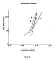
- Figure 3 shows the improved contrast obtained for resists of narrow molecular weight distribution when compared to contrast obtained from broad distribution resists of the same average molecular weight which were identically prepared. Improvement of contrast is due to baking narrow fraction low molecular weight resists above the glass transition temperature.
- Curve D shows the behavior of broad distribution resists having M w/ M n >3 and 80,000 ⁇ M n ⁇ 130,000.
- the slope of the curves shown in Figure 3 can be directly used to calculate contrast of the resists.
- the computed contrast ( ⁇ ) is 6.2, 4.5 and 4.6, respectively.
- Figure 4 illustrates the effect of developer conditions on the improvements in resist sensitivity.
- Curves A and B show the change in dissolution rate of narrowly fractionated 130,000 M n PMMA baked below Tg when developed at 21 and 31 0 C, respectively in a 1:1 MIBK:IPA mixture.
- MIBK solvent
- IPA nonsolvent
Landscapes
- Physics & Mathematics (AREA)
- General Physics & Mathematics (AREA)
- Spectroscopy & Molecular Physics (AREA)
- Addition Polymer Or Copolymer, Post-Treatments, Or Chemical Modifications (AREA)
- Photosensitive Polymer And Photoresist Processing (AREA)
Applications Claiming Priority (4)
| Application Number | Priority Date | Filing Date | Title |
|---|---|---|---|
| US42624382A | 1982-09-28 | 1982-09-28 | |
| US426243 | 1982-09-28 | ||
| US52817883A | 1983-08-31 | 1983-08-31 | |
| US528178 | 1983-08-31 |
Publications (1)
| Publication Number | Publication Date |
|---|---|
| EP0110515A1 true EP0110515A1 (fr) | 1984-06-13 |
Family
ID=27026986
Family Applications (1)
| Application Number | Title | Priority Date | Filing Date |
|---|---|---|---|
| EP83305800A Withdrawn EP0110515A1 (fr) | 1982-09-28 | 1983-09-28 | Méthode pour le contraste et la sensibilité d'un polymère réserve positif, avec température de congélation |
Country Status (3)
| Country | Link |
|---|---|
| EP (1) | EP0110515A1 (fr) |
| AU (1) | AU1962283A (fr) |
| ES (2) | ES8503703A1 (fr) |
Cited By (1)
| Publication number | Priority date | Publication date | Assignee | Title |
|---|---|---|---|---|
| WO1994006058A1 (fr) * | 1992-09-10 | 1994-03-17 | Kernforschungszentrum Karlsruhe Gmbh | Utilisation d'une resine de coulee et son procede de fabrication |
Citations (3)
| Publication number | Priority date | Publication date | Assignee | Title |
|---|---|---|---|---|
| FR1548846A (fr) * | 1967-01-13 | 1968-12-06 | ||
| FR2265809A1 (fr) * | 1974-03-25 | 1975-10-24 | Ibm | |
| FR2394833A1 (fr) * | 1977-06-17 | 1979-01-12 | Thomson Csf | Resine de masquage positive presentant une sensibilite amelioree a l'irradiation electronique, et methode de fabrication d'une telle resine |
-
1983
- 1983-09-23 ES ES525880A patent/ES8503703A1/es not_active Expired
- 1983-09-27 AU AU19622/83A patent/AU1962283A/en not_active Abandoned
- 1983-09-28 EP EP83305800A patent/EP0110515A1/fr not_active Withdrawn
-
1984
- 1984-05-14 ES ES532484A patent/ES532484A0/es active Granted
Patent Citations (3)
| Publication number | Priority date | Publication date | Assignee | Title |
|---|---|---|---|---|
| FR1548846A (fr) * | 1967-01-13 | 1968-12-06 | ||
| FR2265809A1 (fr) * | 1974-03-25 | 1975-10-24 | Ibm | |
| FR2394833A1 (fr) * | 1977-06-17 | 1979-01-12 | Thomson Csf | Resine de masquage positive presentant une sensibilite amelioree a l'irradiation electronique, et methode de fabrication d'une telle resine |
Non-Patent Citations (3)
| Title |
|---|
| EXTENDED ABSTRACTS, The Electrochemical Society, Inc. Fall Meeting, Las Vegas Nevada, 17th-22nd October 1976, vol. 76.2, pages 741-742, abstract no. 288 * |
| FUJITSU SCIENT. & TECHN. JOURNAL, vol. 14, no. 2, June 1978, pages 143-157, Tokyo, JP. * |
| IBM JOURNAL OF RESEARCH AND DEVELOPMENT, vol. 12, no. 3, May 1968, pages 251-256, New York, USA * |
Cited By (1)
| Publication number | Priority date | Publication date | Assignee | Title |
|---|---|---|---|---|
| WO1994006058A1 (fr) * | 1992-09-10 | 1994-03-17 | Kernforschungszentrum Karlsruhe Gmbh | Utilisation d'une resine de coulee et son procede de fabrication |
Also Published As
| Publication number | Publication date |
|---|---|
| ES8600346A1 (es) | 1985-09-16 |
| ES532484A0 (es) | 1985-09-16 |
| ES525880A0 (es) | 1985-03-01 |
| ES8503703A1 (es) | 1985-03-01 |
| AU1962283A (en) | 1984-04-05 |
Similar Documents
| Publication | Publication Date | Title |
|---|---|---|
| US4061829A (en) | Negative resist for X-ray and electron beam lithography and method of using same | |
| CA1088737A (fr) | Mode de fabrication d'une matiere de protection durcie par rayonnement energetique eleve | |
| US4267258A (en) | Negative type deep ultraviolet resist | |
| US4430419A (en) | Positive resist and method for manufacturing a pattern thereof | |
| US5403699A (en) | Process for formation of resist patterns | |
| CA1176902A (fr) | Obtention de structures protectrices grace a des ondes courtes uv et d'un copolymere renfermant un derive acrylique chlore ou cyane | |
| EP0240843B1 (fr) | Composition photosensible, son procédé de préparation et emploi | |
| US4608281A (en) | Improvements in sensitivity of a positive polymer resist having a glass transition temperature through control of a molecular weight distribution and prebaked temperature | |
| US4701342A (en) | Negative resist with oxygen plasma resistance | |
| JPS5983157A (ja) | ポジ型重合体レジストの感度及びコントラストを増大させる方法 | |
| EP0110515A1 (fr) | Méthode pour le contraste et la sensibilité d'un polymère réserve positif, avec température de congélation | |
| US4604305A (en) | Improvements in contrast of a positive polymer resist having a glass transition temperature through control of the molecular weight distribution and prebaked temperature | |
| US4454200A (en) | Methods for conducting electron beam lithography | |
| US5589424A (en) | Photodefinable dielectric layers comprising poly(aromatic diacetylenes) | |
| JPH0643646A (ja) | フォトレジスト組成物 | |
| US4414313A (en) | Sensitive positive electron beam resists | |
| JPS59198446A (ja) | 感光性樹脂組成物及びその使用方法 | |
| JPS63271253A (ja) | 高解像度ポジ型放射線感応性レジスト | |
| US4302529A (en) | Process for developing a positive electron resist | |
| Novembre et al. | A sub‐0.5 μm bilevel lithographic process using the deep‐UV electron‐beam resist p (si‐cms) | |
| JPS60260946A (ja) | パタ−ン形成用材料及びパタ−ン形成方法 | |
| JPH0358104B2 (fr) | ||
| JPH087441B2 (ja) | ポジ型高感度放射線感応性レジスト | |
| JPS59121042A (ja) | ネガ型レジスト組成物 | |
| Deckman et al. | PMMA electron resists with narrow molecular weight distribution |
Legal Events
| Date | Code | Title | Description |
|---|---|---|---|
| PUAI | Public reference made under article 153(3) epc to a published international application that has entered the european phase |
Free format text: ORIGINAL CODE: 0009012 |
|
| AK | Designated contracting states |
Designated state(s): BE DE FR GB IT |
|
| 17P | Request for examination filed |
Effective date: 19841115 |
|
| 17Q | First examination report despatched |
Effective date: 19860520 |
|
| D17Q | First examination report despatched (deleted) | ||
| STAA | Information on the status of an ep patent application or granted ep patent |
Free format text: STATUS: THE APPLICATION IS DEEMED TO BE WITHDRAWN |
|
| 18D | Application deemed to be withdrawn |
Effective date: 19880510 |
|
| RIN1 | Information on inventor provided before grant (corrected) |
Inventor name: DECKMAN, HARRY WILLIAM Inventor name: DUNSMUIR, JOHN HENRY |