EP0111086A2 - Procédé pour la fabrication de structures à dimensions sub-micrométriques et application de ce procédé pour la fabrication de régions d'isolation diélectrique profondes à largeur sub-micrométrique dans un corps semi-conducteur - Google Patents
Procédé pour la fabrication de structures à dimensions sub-micrométriques et application de ce procédé pour la fabrication de régions d'isolation diélectrique profondes à largeur sub-micrométrique dans un corps semi-conducteur Download PDFInfo
- Publication number
- EP0111086A2 EP0111086A2 EP83109945A EP83109945A EP0111086A2 EP 0111086 A2 EP0111086 A2 EP 0111086A2 EP 83109945 A EP83109945 A EP 83109945A EP 83109945 A EP83109945 A EP 83109945A EP 0111086 A2 EP0111086 A2 EP 0111086A2
- Authority
- EP
- European Patent Office
- Prior art keywords
- layer
- silicon
- silicon dioxide
- mask
- reactive ion
- Prior art date
- Legal status (The legal status is an assumption and is not a legal conclusion. Google has not performed a legal analysis and makes no representation as to the accuracy of the status listed.)
- Granted
Links
Images


Classifications
-
- H—ELECTRICITY
- H10—SEMICONDUCTOR DEVICES; ELECTRIC SOLID-STATE DEVICES NOT OTHERWISE PROVIDED FOR
- H10P—GENERIC PROCESSES OR APPARATUS FOR THE MANUFACTURE OR TREATMENT OF DEVICES COVERED BY CLASS H10
- H10P76/00—Manufacture or treatment of masks on semiconductor bodies, e.g. by lithography or photolithography
- H10P76/40—Manufacture or treatment of masks on semiconductor bodies, e.g. by lithography or photolithography of masks comprising inorganic materials
- H10P76/408—Manufacture or treatment of masks on semiconductor bodies, e.g. by lithography or photolithography of masks comprising inorganic materials characterised by their sizes, orientations, dispositions, behaviours or shapes
- H10P76/4085—Manufacture or treatment of masks on semiconductor bodies, e.g. by lithography or photolithography of masks comprising inorganic materials characterised by their sizes, orientations, dispositions, behaviours or shapes characterised by the processes involved to create the masks
-
- H—ELECTRICITY
- H10—SEMICONDUCTOR DEVICES; ELECTRIC SOLID-STATE DEVICES NOT OTHERWISE PROVIDED FOR
- H10P—GENERIC PROCESSES OR APPARATUS FOR THE MANUFACTURE OR TREATMENT OF DEVICES COVERED BY CLASS H10
- H10P50/00—Etching of wafers, substrates or parts of devices
- H10P50/69—Etching of wafers, substrates or parts of devices using masks for semiconductor materials
- H10P50/691—Etching of wafers, substrates or parts of devices using masks for semiconductor materials for Group V materials or Group III-V materials
- H10P50/693—Etching of wafers, substrates or parts of devices using masks for semiconductor materials for Group V materials or Group III-V materials characterised by their size, orientation, disposition, behaviour or shape, in horizontal or vertical plane
- H10P50/695—Etching of wafers, substrates or parts of devices using masks for semiconductor materials for Group V materials or Group III-V materials characterised by their size, orientation, disposition, behaviour or shape, in horizontal or vertical plane characterised by the process involved to create the mask, e.g. lift-off masks or sidewalls or to modify the mask
-
- H—ELECTRICITY
- H10—SEMICONDUCTOR DEVICES; ELECTRIC SOLID-STATE DEVICES NOT OTHERWISE PROVIDED FOR
- H10P—GENERIC PROCESSES OR APPARATUS FOR THE MANUFACTURE OR TREATMENT OF DEVICES COVERED BY CLASS H10
- H10P50/00—Etching of wafers, substrates or parts of devices
- H10P50/69—Etching of wafers, substrates or parts of devices using masks for semiconductor materials
- H10P50/691—Etching of wafers, substrates or parts of devices using masks for semiconductor materials for Group V materials or Group III-V materials
- H10P50/693—Etching of wafers, substrates or parts of devices using masks for semiconductor materials for Group V materials or Group III-V materials characterised by their size, orientation, disposition, behaviour or shape, in horizontal or vertical plane
- H10P50/696—Process specially adapted to improve the resolution of the mask
-
- H—ELECTRICITY
- H10—SEMICONDUCTOR DEVICES; ELECTRIC SOLID-STATE DEVICES NOT OTHERWISE PROVIDED FOR
- H10P—GENERIC PROCESSES OR APPARATUS FOR THE MANUFACTURE OR TREATMENT OF DEVICES COVERED BY CLASS H10
- H10P76/00—Manufacture or treatment of masks on semiconductor bodies, e.g. by lithography or photolithography
- H10P76/40—Manufacture or treatment of masks on semiconductor bodies, e.g. by lithography or photolithography of masks comprising inorganic materials
- H10P76/408—Manufacture or treatment of masks on semiconductor bodies, e.g. by lithography or photolithography of masks comprising inorganic materials characterised by their sizes, orientations, dispositions, behaviours or shapes
- H10P76/4088—Processes for improving the resolution of the masks
-
- H—ELECTRICITY
- H10—SEMICONDUCTOR DEVICES; ELECTRIC SOLID-STATE DEVICES NOT OTHERWISE PROVIDED FOR
- H10W—GENERIC PACKAGES, INTERCONNECTIONS, CONNECTORS OR OTHER CONSTRUCTIONAL DETAILS OF DEVICES COVERED BY CLASS H10
- H10W10/00—Isolation regions in semiconductor bodies between components of integrated devices
- H10W10/01—Manufacture or treatment
- H10W10/011—Manufacture or treatment of isolation regions comprising dielectric materials
- H10W10/014—Manufacture or treatment of isolation regions comprising dielectric materials using trench refilling with dielectric materials, e.g. shallow trench isolations
-
- H—ELECTRICITY
- H10—SEMICONDUCTOR DEVICES; ELECTRIC SOLID-STATE DEVICES NOT OTHERWISE PROVIDED FOR
- H10W—GENERIC PACKAGES, INTERCONNECTIONS, CONNECTORS OR OTHER CONSTRUCTIONAL DETAILS OF DEVICES COVERED BY CLASS H10
- H10W10/00—Isolation regions in semiconductor bodies between components of integrated devices
- H10W10/10—Isolation regions comprising dielectric materials
- H10W10/17—Isolation regions comprising dielectric materials formed using trench refilling with dielectric materials, e.g. shallow trench isolations
-
- Y—GENERAL TAGGING OF NEW TECHNOLOGICAL DEVELOPMENTS; GENERAL TAGGING OF CROSS-SECTIONAL TECHNOLOGIES SPANNING OVER SEVERAL SECTIONS OF THE IPC; TECHNICAL SUBJECTS COVERED BY FORMER USPC CROSS-REFERENCE ART COLLECTIONS [XRACs] AND DIGESTS
- Y10—TECHNICAL SUBJECTS COVERED BY FORMER USPC
- Y10S—TECHNICAL SUBJECTS COVERED BY FORMER USPC CROSS-REFERENCE ART COLLECTIONS [XRACs] AND DIGESTS
- Y10S438/00—Semiconductor device manufacturing: process
- Y10S438/942—Masking
- Y10S438/947—Subphotolithographic processing
Definitions
- the invention relates to a method for producing structures with dimensions in the submicron range and the use of this method for producing a deep dielectric insulation with a submicron width in a silicon body.
- a number of methods are known for increasing the integration density of integrated circuits. Significant increases in the integration density have recently been achieved primarily by reducing the density of photolithographic defects. The use of electron and X-ray exposure methods instead of the previously used light radiation has made progress towards a higher optical resolution. In addition, efforts have been made to achieve very narrow line widths in the range of 1 ⁇ m and below by expanding standard lithographic techniques while avoiding the costly techniques of electron and X-ray lithography. With the technology of plasma or reactive ion etching for etching metals, semiconducting and dielectric materials, further progress towards very narrow line widths and thus a higher integration density could be made.
- U.S. Patent 4,358,340 describes a method of making submicron devices, but without using submicron lithography, in which a conductive thin film with dimensions in the submicron range is deposited on a vertical step between adjacent surfaces of an insulation and then vertically etched to the conductive film only has the part that is in contact with the vertical step. The remaining insulation not covered by the conductor is removed to obtain a gate of a MOS field effect transistor with a width in the submicron range which is equal to the layer thickness of the thin film originally applied.
- US Pat. No. 4,209,349 describes a method for forming very small mask openings for the production of semiconductor circuit arrangements.
- regions of a first insulating layer are first formed on a substrate, so that there are essentially horizontal and essentially vertical surfaces.
- a second insulating layer made of different material than the first insulating layer is applied, and a reactive ion etching method is applied in this way subjected in that the horizontal portions of the second insulating layer are removed and only very narrow regions of this layer on the vertically ge - remain directed surface regions of the first insulating layer or the relevant areas of the substrate.
- a thermal oxidation of the exposed substrate areas is then carried out and the areas of the second insulating layer located there are finally removed to expose the desired mask openings.
- This process is said to be able to achieve smaller dimensions than the minimum dimensions previously determined with conventional photolithographic processes.
- the first insulating layer determines the position and thickness of the mask (column 2, line 62). All openings in the insulating layer are made by standard photolithography and etching techniques (column 3, line 21), in which no vertical side walls can be obtained. In the method according to the invention, however, a polymer layer determines the position and thickness of the mask. In the process of the US patent, hot processes are carried out throughout, for example thermal oxidation at 970 ° C. (column 4, line 65) and the deposition of silicon nitride from the gas phase at approximately 1000 ° C.
- the thermal oxidation results in an asymmetrical mask in which the bird's beak problem, which arises due to the formation of a non-planar silicon dioxide on the surface of the trench, plays a role, so that the mask is also removed is therefore unusable for etching trenches.
- the mask produced according to the invention has strictly vertical side walls and is constructed symmetrically.
- junction isolation in which isolation wells are formed by surrounding semiconductor areas with oppositely doped semiconductor zones.
- the resulting semiconductor junctions form diodes operated in the reverse direction, which bring about the insulation.
- dielectric insulation in this, the semiconductor regions to be insulated are surrounded with a dielectric insulation trough. In one embodiment of the same, trenches are formed in silicon, in which the isolation regions are then formed.
- the remaining surface of the semiconductor substrate is protected by a protective layer which consists of a silicon dioxide-silicon nitride sandwich structure.
- a protective layer which consists of a silicon dioxide-silicon nitride sandwich structure.
- the silicon semiconductor substrate is subjected to oxidation in a conventional manner, as a result of which the silicon in the region of the trenches is oxidized and the resulting silicon dioxide fills the trenches.
- undesirable structures are formed on the edges of the trenches, which are referred to as "bird's beak".
- Bird's beak refers to the formation of a non-planar silicon dioxide on the surface of the trench, which is caused by the lateral oxidation which takes place below the silicon dioxide layer and causes the silicon dioxide / silicon nitride structure to bulge at the edges of the trench. As a result, it is no longer possible to directly adjoin diffusions to the insulation, which represents a significant advantage of the dielectric insulation originally planned.
- An alternative to the embedded oxide insulation is "deep dielectric insulation, which includes the formation of rectangular trenches by reactive ion etching processes and the filling of the trenches to form the insulation for the individual silicon regions of the substrate.
- This process also has some significant disadvantages.
- Solk for example for No thermal oxide is used to fill the trenches, but only an oxide which is chemically deposited from a gas phase containing silane and oxygen, or polysilicon. Filling the trenches with oxide by chemical deposition from the gas phase can in turn lead to poor oxide quality or a seam line in the middle of the trenches, which can influence the continuity of the metallic conductor run on the surface and ultimately cause conductivity errors.
- the oxide chemically separated from the gas phase does not have the same thermal expansion coefficient as silicon during the subsequent different temperature processes and leads to stresses around the trenches at process temperatures around 1000 ° C. Furthermore, oxide chemically separated from the gas phase is difficult to planarize.
- the invention achieves the object of specifying an improved lithography method with reduced line widths down to the submicron range.
- the invention also relates to the use of this method for producing deep dielectric insulation with widths in the submicron range.
- a structure is made from polymer material with vertical sidewalls, the latter being used to form sidewall structures of silicon oxide or nitride with dimensions in the submicron range.
- These side wall structures can be used directly as masks.
- a further layer is alternatively applied over the side wall structures, this is removed until the tips of the side wall structures are exposed and the same is removed. The resulting opening can then be used as a mask for a large number of processes for producing integrated circuits.
- the invention also includes an application of the method for producing submicron-wide deep dielectric insulation in a silicon semiconductor body.
- the method according to the invention can be used to produce silicon dioxide etching masks with openings which are only 0.2 ⁇ m wide and have vertical side walls. These in turn are used to etch trenches into the silicon substrate with a width of 0.5 ⁇ m. The trenches are then filled with dielectric material.
- the lithography method according to the invention is described in general with reference to FIGS. 3 to 9 and 14 and 15 and subsequently the production of deep dielectric insulation in a silicon semiconductor body using a special exemplary embodiment (FIGS. 10 to 13).
- a layer 2 of dielectric material is applied to a silicon semiconductor substrate by conventional methods.
- Layer 2 can consist, for example, of silicon dioxide, which is produced by thermal oxidation at 925 ° C.
- Layer 2 can also consist of a silicon dioxide layer and a silicon nitride layer, the silicon dioxide layer having a layer thickness of approximately 160 nm and the silicon nitride layer having a layer thickness of approximately 100 nm.
- the silicon dioxide layer is produced in a conventional manner by thermal oxidation, and the silicon nitride layer is deposited in a known manner from an atmosphere containing silane, ammonia and argon at a temperature of approximately 1000 ° C.
- a double layer made of silicon dioxide and polysilicon or polysilicon and silicon dioxide can also be applied.
- Layer 2 can also be constructed from a sequence of layers, which is discussed in detail in connection with FIG. 14. It is also possible to apply the following layers to the bare surface of the silicon substrate 1.
- Layer 2 is used to produce a structure of polymer material with vertical side walls Polymer, for example a polyimide, which is thermally stable up to about 400 to 450 ° C, spun on. It should be emphasized that the layer thickness of the polymer material determines the height of the silicon nitride or silicon dioxide walls which are produced in the further course of the process. A number of known positive or negative resist materials can also be applied as polymer materials in the desired layer thickness, for example of approximately 2.0 ⁇ m.
- a positive resist material for example, a resist from Shipley, which is available under the trade name 1350J and consists of a phenol formaldehyde resin and a naphthoquinonediazide sensitizer, which is used as 3,4-dihydroxybenzophenone-4- [naphthoquinone (1,2) diazide (2)] sulfonate is used.
- the resist layer 3 is cured at a temperature which is the same as or higher than the deposition temperature of the material 6 to form the side wall structure (FIG. 5).
- the resist layer 3 made of the aforementioned material can, for example, be cured at a temperature of 210 ° C. for about 30 minutes.
- a silicon nitride layer 4 is applied to the resist layer 3 as an etching barrier for reactive ion etching with oxygen in a layer thickness of approximately 100 nm.
- the silicon nitride is deposited by plasma deposition from an atmosphere containing silane, ammonia and argon at a pressure of about 1 mbar and a power of 100 watts (power density 0.05 W / cm 2 ). The time required for this is about 3 to 4 minutes. It should be emphasized that the deposition temperature is 210 ° C., ie it is a so-called "cold process" in which the material of layer 3 is not damaged.
- a resist layer 5 is applied to the plasma silicon nitride layer 4 in a layer thickness of approximately 1.0 ⁇ m.
- Layer 5 can consist of the same resist material as layer 3. However, it can also consist of another photoresist which is highly sensitive to radiation, for example a methacrylate resist.
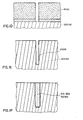
- a pattern is produced in layer 5 by exposure and development. Then, as shown in FIG. 4 and SEM 1, a resist mask 3 with edge angles that are as steep as possible is generated by reactive ion etching. For the production of the desired mask structure with the steepest possible edge angles, it is a prerequisite that these resist side walls are as steep as possible.
- top resist layer 5 As a mask, 4 openings are etched into the plasma nitride layer.
- the nitride layer 4 and the underlying polymer or resist layer 3 are etched by reactive ions.
- the plasma nitride layer 4 is etched in a reactor with carbon tetrafluoride under the following conditions:
- the etching rate for plasma nitride is approximately 30 nm / min under these conditions.
- the layer 4 with the etched openings is used as a mask for etching the resist or polymer layer 3.
- Layer 3 is etched with oxygen in a reactive ion etching process under the following conditions:
- the etch rate for a resist is approximately 150 nm / min under these conditions.
- the reactive ion etching is carried out at a very low oxygen pressure of approximately 2 to 5 ⁇ bar. If one were to work at a higher oxygen pressure, the proportion of lateral etching which would be noticeable in a lateral undercut of the silicon nitride mask would increase.
- Residues of plasma nitride and resist are removed in a known manner by etching with buffered hydrofluoric acid.
- PCT application WO 80/00639 Western Electric, US priority September 11, 1978 (Serial No. 941 369).
- the structure made of polymer material 3 with vertical side walls can also be produced in a modified image reversal process (DE patent 25 29 054) (not shown). This process is inexpensive and inexpensive. This also results in structures with almost vertical side walls. Specifically, a photosensitive layer which contains a phenol-formaldehyde resin, an o-quinonediazide and a 1-hydroxyethyl-2-alkylimidazoline (monazoline C) is applied to the substrate 1, 2 in accordance with to produce a negative resist image. Fig. 3 applied.
- This layer is exposed imagewise and then Heated to about 105 ° C for 10 to 20 minutes.
- the photoresist is crosslinked by the monazoline molecules in the exposed areas, as a result of which these areas become insoluble in an alkaline developer.
- the entire photoresist layer is exposed. With this full-area exposure, the photoresist is now also decomposed in the areas not exposed during the image-wise exposure, while no significant change takes place in the exposed areas.
- a resist image which is negative for presentation is obtained.
- FIGS. 5 and 6 (SEM 2- and 3) show the plasma deposition of silicon nitride 6 on the horizontal and vertical surfaces of the resist structure 3 and the substrate 2 and the production of plasma nitride walls by removing the nitride from all horizontal surfaces by reactive ion etching and , also by reactive ion etching, the removal of the resist 3.
- silicon dioxide or polysilicon can also be deposited from the vapor phase at low temperature on the horizontal and vertical surfaces of the resist structure.
- silicon nitride 6 is deposited from a plasma of an atmosphere containing silane, ammonia and argon at a pressure of 1 mbar and an output of 100 watts at a temperature of 210 ° C. in a layer thickness of approximately 400 nm.
- the silicon nitride 6 be covers all horizontal and vertical surfaces of the resist structure 3 and the substrate 2 (SEM 2).
- the silicon nitride is then removed from all horizontal surfaces by reactive ion etching in carbon tetrafluoride. This is done, for example, with a CF4 flow of 30 cm 3 / min., A pressure of about 50 ⁇ bar and a power density of 0.2 W / cm 2 .
- CF 4 etching is stopped when all silicon nitride is removed from the horizontal surfaces.
- the end point of the etching is determined with laser interference with 5 to 10% overetching.
- the procedure is analogous if the deposited material consists of silicon dioxide or polysilicon.
- the resist 3 is removed by reactive ion etching in an oxygen-containing atmosphere. It is not necessary to maintain a particularly low oxygen pressure in this step.
- the actual mask material is then deposited (FIG. 7A).
- Any materials that can be applied by spinning such as a photoresist, polyimide or glass, or materials that can be sputtered on or deposited from the vapor phase, for example silicon dioxide, silicon nitride, magnesium oxide, polysilicon, aluminum oxide, metals, are suitable as such and the same.
- silicon dioxide is selected as the mask material, this can be done by sputtering, by deposition from a silane and oxygen-containing gas plasma or by chemical precipitation from an SiH 4 and oxygen or SiH 2 Cl 2 and N 2 0-containing gas atmosphere can be applied.
- the different deposition methods each result in a different form of the silicon dioxide which covers the plasma silicon nitride walls 6.
- silicon dioxide for example by means of sputtering.
- This method is the preferred in the context of the present invention. First, about 1.3 ⁇ m silicon dioxide (standard quartz) is applied using standard sputtering techniques. Then an approximately 0.5 ⁇ m thick silicon dioxide layer (planar quartz) is applied in a planar process by means of cathode sputtering with increased anode performance. In this method, silicon dioxide is removed simultaneously during application, as a result of which structures with a surface topology are essentially planarized (FIG. 7A).
- FIGS. 7B and 7C Further possibilities for covering the silicon nitride walls 6 with silicon dioxide are shown in FIGS. 7B and 7C.
- a 0.5 ⁇ m thick silicon dioxide layer 7a is deposited on the entire surface of the structure with the silicon nitride walls 6 by means of chemical precipitation from the gas phase.
- Chemical vapor deposition uses S i H4 and O 2 at about 500 ° C or SiH 2 Cl 2 and N 2 0 at about 800 ° C and atmospheric pressure or less.
- an approximately 1 ⁇ m thick silicon dioxide layer is applied with increased anode power by means of cathode sputtering (planar quartz).
- the silicon dioxide 7b applied by means of sputtering causes one Increasing the silicon dioxide layer thickness and a planarization of the areas over the silicon nitride walls 6 (FIG. 7B).
- a photoresist can also be applied as layer 7b for planarization and cured at 180 ° C.
- FIG. 7 Another way to planarize a structure as shown in FIG. 7 is to deposit and etch quartz under the usual sputtering conditions until the tips of the silicon nitride walls 6 are exposed (FIG. 7C).
- a planarization of the structure can, as already indicated in the planarization according to FIG. 7B, be carried out in such a way that instead of the quartz applied by means of sputtering, a photoresist is applied in a layer thickness of 2.0 gm ′ and cured at 180 ° C. and then etching away from the resist layer until the tips of the silicon nitride walls are exposed (FIG. 7C).
- the silicon nitride walls embedded in silicon dioxide as mask material are removed by etching.
- the entire surface of the silicon dioxide is removed in a layer thickness of about 0.3 ⁇ m by reactive ion etching with CF 4 .
- the silicon nitride walls are plasma-etched in a LFE Corporation system using carbon tetrafluoride at a pressure of approximately 1.0 mbar to obtain openings 8 with a width of 0.2 to 0.3 ⁇ m, which extend to the SiO 2 layer 2 range, removed.
- the silicon nitride walls can also be removed by wet etching. According to FIG.
- the openings 8 of the silicon dioxide mask are deepened through the entire surface reactive ion etching with CF 4 through the layer 2 up to the silicon substrate 1.
- This The step can also be carried out with CHF 3 gas, since this ensures a better interruption of the etching on the silicon substrate surface.
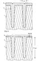
- Silicon dioxide is also removed from the surface of the mask during the etching. If the walls 6, which define the height and width of the mask openings 8, are made of silicon dioxide or polysilicon, a photoresist must be used for planarization. In the case of walls made of polysilicon, quartz can also be planarized. The silicon dioxide or polysilicon walls 6 are removed by wet etching until the layer 2, which in this case consists of silicon nitride, is reached. FIG.
- SEM 5 shows the finished etching mask made of silicon dioxide 7, which can be used for etching trenches in silicon substrate 1. It has a thickness of approximately 0.6 to 1 ⁇ m and openings with almost vertical side walls and a width of 0.2 to 0.3 ⁇ m.
- FIGS. 14 and 15 a method is described with which the side walls 6 can be converted into a positive template with identical dimensions but made of a different material.
- layer 2 of the figures described above consists of a double layer, a layer 2a of the desired mask material, for example of a photoresist, of polyimide, silicon dioxide, silicon nitride, polysilicon, metal or combinations of these materials and a thin, dielectric layer 2b, which is based on layer 2a is arranged and. made of plasma nitride or Oxide exists.
- a series of layers, for example of silicon dioxide, polyimide, silicon dioxide, can also take the place of the layer.
- the sidewall structures 6 with the submicron dimensions, as described above, are produced with the aid of a structure made of polymer material with vertical sidewalls.
- the dielectric layer 2b which in the case of side walls made of plasma nitride made of silicon dioxide, is removed by reactive ion etching in carbon tetrafluoride.
- Layer 2a is also removed in the areas not covered by side walls 6 by reactive ion etching. If the layer 2a consists of polymer material, the reactive ion etching can be carried out in an atmosphere of oxygen.
- the side wall structures 6 and the remaining silicon dioxide of the layer 2b are then removed by LFE etching or wet etching.
- a positive mask structure with the dimensions of the plasma nitride columns according to FIG. 6 is obtained, which however consist of the material of layer 2a (FIGS. 14 and 15).
- the layer 2 of FIG. 14 consists of a sequence of layers of, for example, silicon dioxide, polyimide, silicon dioxide, then after the production of the submicron mask 6, the uppermost thin oxide layer in a CF 4 atmosphere, the polyimide in an oxygen atmosphere and the silicon dioxide on the surface of the Silicon substrate etched in a CF 4 atmosphere with reactive ions.
- the final silicon dioxide mask is obtained on the silicon substrate by plasma etching in oxygen or by dissolving the middle polyimide layer of the etched structures.
- FIG. 6 A special application of the previously described method is shown below, in which in a Mask reversal method, the structures shown in FIG. 6 can be used to produce a silicon dioxide mask 7.
- trenches are etched into a silicon substrate.
- the trenches are filled by thermal oxidation or by spinning on a plastic, for example polyimide.
- a semiconductor wafer made of p- conducting material can be used as the silicon substrate.
- This substrate with a resistivity of 10 ⁇ -cm, in which an N + conductive zone was produced (not shown), is applied in a conventional process at a temperature in the range between 950 and 1170 ° C. and for a period of about 17 minutes an N conductive layer with a maximum interfering element concentration of 10 18 atoms / cm 3 epitaxially grown. During the deposition of this layer, the N + conductive zone diffuses out into this layer.
- the epitaxial layer 1 (FIG.
- Epitaxial layer-1 can be applied, for example, using an apparatus and method as described in U.S. Patent 3,424,629. 3, a layer 2 of dielectric material is then applied to the epitaxial layer 1 by conventional methods.
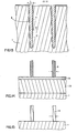
- SEM 6 shows the production of the trenches 9 in the silicon substrate 1 by etching.
- the reactive ion etching which is carried out for this purpose, takes place under the following conditions:
- etching silicon uses gas mixtures containing SF 6 , C1 2 and helium or CC1 2 F 2 and 0 2 or SiF 4 , C1 2 , helium or argon.
- chlorine, fluorine and / or oxygen-containing gas mixtures can be used for reactive ion etching of silicon.
- the Leybold etching rate ratios of silicon to silicon dioxide of up to 20: 1. If deep and shallow trenches are to be etched at the same time, then the previously described etching process must be carried out twice, or a mask must be used with which the shallow trenches are covered during the further etching of the deep trenches. 10, the remaining silicon dioxide etching mask is removed in a wet etching step with buffered hydrofluoric acid.
- FIG. 11 shows the filling of the trenches by thermal oxidation. This takes place at about 1000 ° C. and is carried out as dry-wet-dry oxidation until about 0.5 ⁇ m silicon dioxide has formed in the trenches from each trench wall and a silicon dioxide of comparable layer thickness has formed on the surface.
- the oxidation can also be carried out in the form of a high pressure oxidation at 850 ° C.
- the oxide in FIG. 11 removed by reactive ion etching over the entire surface in CHF 3 with interruption of the etching on the silicon surface. The silicon is then reoxidized
- the interface between the insulation and the silicon substrate has a low charge level due to the thermal oxidation.
- the filling of the trenches with polyimide instead of the filling by thermal oxidation is particularly advantageous because defects in the silicon were observed in the case of trenches completely filled with thermal oxide. When filling with oxide separated from the gas phase, such defects can be largely avoided.
- the diffusions from the sub-collector, base and emitter can directly connect to the insulation, the formation of the undesirable "bird beaks" is also avoided.
- the trenches are etched after the diffusion of subcollector, base and emitter.
- the quality of the arrangements produced using the method according to the invention is improved on account of the lower capacitance, which is due to the direct connection of the diffusions to the insulation and shorter electrical conduction paths.
- the method according to the invention for producing structures with dimensions in the submicron range uses polymer materials instead of dielectric materials to define structures with horizontal and vertical surfaces, for example a photoresist or polyimide.
- the polymer materials can be applied in a simple and inexpensive process by spinning. They can be excellently etched vertically with reactive oxygen ions, in particular using the three-layer process described.
- the polymer layer which determines the position and the thickness of the mask, can be applied with a much greater layer thickness than, for example, dielectric materials. Therefore, masks can be made with a greater thickness than would be possible with other processes. With masks that have a thickness of, for example, up to 3 ⁇ m, trenches up to 6 ⁇ m deep can be etched into a silicon substrate.
- the sidewall structures are produced from silicon dioxide or silicon nitride in a plasma deposition process, which can be carried out at temperatures> 200 ° C. and is a so-called low-temperature process, so that the polymer structures are not damaged.
- the lower process temperatures compared to the prior art also allow the process to be used more universally.
- the method according to the invention is not only suitable for producing deep dielectric insulation with a trench width in the submicron range. Other possible applications are, for example, the production of field effect transistors with a channel length in the submicrometer range or the production of lateral, bipolar pnp transistors with a base width in the submicrometer range.
Landscapes
- Drying Of Semiconductors (AREA)
- Element Separation (AREA)
- ing And Chemical Polishing (AREA)
Applications Claiming Priority (2)
| Application Number | Priority Date | Filing Date | Title |
|---|---|---|---|
| DE3242113 | 1982-11-13 | ||
| DE19823242113 DE3242113A1 (de) | 1982-11-13 | 1982-11-13 | Verfahren zur herstellung einer duennen dielektrischen isolation in einem siliciumhalbleiterkoerper |
Publications (3)
| Publication Number | Publication Date |
|---|---|
| EP0111086A2 true EP0111086A2 (fr) | 1984-06-20 |
| EP0111086A3 EP0111086A3 (en) | 1986-07-30 |
| EP0111086B1 EP0111086B1 (fr) | 1989-03-08 |
Family
ID=6178117
Family Applications (1)
| Application Number | Title | Priority Date | Filing Date |
|---|---|---|---|
| EP83109945A Expired EP0111086B1 (fr) | 1982-11-13 | 1983-10-05 | Procédé pour la fabrication de structures à dimensions sub-micrométriques et application de ce procédé pour la fabrication de régions d'isolation diélectrique profondes à largeur sub-micrométrique dans un corps semi-conducteur |
Country Status (4)
| Country | Link |
|---|---|
| US (1) | US4502914A (fr) |
| EP (1) | EP0111086B1 (fr) |
| JP (1) | JPS59107518A (fr) |
| DE (2) | DE3242113A1 (fr) |
Cited By (10)
| Publication number | Priority date | Publication date | Assignee | Title |
|---|---|---|---|---|
| EP0146789A3 (en) * | 1983-12-29 | 1988-03-16 | International Business Machines Corporation | Process for forming isolating trenches in integrated circuit devices |
| FR2607600A1 (fr) * | 1986-11-28 | 1988-06-03 | Commissariat Energie Atomique | Procede de realisation sur un substrat d'elements espaces les uns des autres |
| WO1988005602A1 (fr) * | 1987-01-26 | 1988-07-28 | Commissariat A L'energie Atomique | Procede de fabrication de zones d'isolation electrique dans un circuit integre cmos |
| EP0226517A3 (fr) * | 1985-12-18 | 1989-10-18 | Fairchild Semiconductor Corporation | Procédé pour isoler des régions ayant des concentrations d'impuretés différentes dans un substrat semi-conducteur |
| EP0369053A1 (fr) * | 1988-11-17 | 1990-05-23 | International Business Machines Corporation | Procédé pour fabriquer des masques comportant des structures dans la région submicrométrique |
| EP0223032A3 (fr) * | 1985-11-18 | 1990-06-27 | International Business Machines Corporation | Procédé pour la formation d'ouvertures de masque submicronique utilisant les techniques de décollage et utilisation d'écarteurs accolés |
| EP0402296A1 (fr) * | 1989-06-09 | 1990-12-12 | International Business Machines Corporation | Transistor à effet de champ ayant une structure asymétrique |
| EP0313814A3 (fr) * | 1987-10-30 | 1991-01-02 | International Business Machines Corporation | Structures de flancs en matière organique |
| EP0288739A3 (fr) * | 1987-04-30 | 1991-01-16 | International Business Machines Corporation | Procédé de self-alignement d'une structure de tranchée d'isolation par rapport à une région implantée |
| WO1998018165A1 (fr) * | 1996-10-18 | 1998-04-30 | Siemens Aktiengesellschaft | Cellule de memoire et procede de fabrication d'une cellule de memoire remanente |
Families Citing this family (149)
| Publication number | Priority date | Publication date | Assignee | Title |
|---|---|---|---|---|
| JPS60173842A (ja) * | 1984-02-20 | 1985-09-07 | Canon Inc | パタ−ン形成方法 |
| US4663832A (en) * | 1984-06-29 | 1987-05-12 | International Business Machines Corporation | Method for improving the planarity and passivation in a semiconductor isolation trench arrangement |
| US4596070A (en) * | 1984-07-13 | 1986-06-24 | Texas Instruments Incorporated | Interdigitated IMPATT devices |
| US4599136A (en) * | 1984-10-03 | 1986-07-08 | International Business Machines Corporation | Method for preparation of semiconductor structures and devices which utilize polymeric dielectric materials |
| US4568601A (en) * | 1984-10-19 | 1986-02-04 | International Business Machines Corporation | Use of radiation sensitive polymerizable oligomers to produce polyimide negative resists and planarized dielectric components for semiconductor structures |
| US4631803A (en) * | 1985-02-14 | 1986-12-30 | Texas Instruments Incorporated | Method of fabricating defect free trench isolation devices |
| JPS6269520A (ja) * | 1985-09-21 | 1987-03-30 | Semiconductor Energy Lab Co Ltd | 光cvd法により凹部を充填する方法 |
| US5462767A (en) * | 1985-09-21 | 1995-10-31 | Semiconductor Energy Laboratory Co., Ltd. | CVD of conformal coatings over a depression using alkylmetal precursors |
| US4689871A (en) * | 1985-09-24 | 1987-09-01 | Texas Instruments Incorporated | Method of forming vertically integrated current source |
| US4661204A (en) * | 1985-10-25 | 1987-04-28 | Tandem Computers Inc. | Method for forming vertical interconnects in polyimide insulating layers |
| US4753901A (en) * | 1985-11-15 | 1988-06-28 | Ncr Corporation | Two mask technique for planarized trench oxide isolation of integrated devices |
| EP0238690B1 (fr) * | 1986-03-27 | 1991-11-06 | International Business Machines Corporation | Procédé pour la formation de flancs latéraux |
| US4726879A (en) * | 1986-09-08 | 1988-02-23 | International Business Machines Corporation | RIE process for etching silicon isolation trenches and polycides with vertical surfaces |
| US4707218A (en) | 1986-10-28 | 1987-11-17 | International Business Machines Corporation | Lithographic image size reduction |
| US5082795A (en) * | 1986-12-05 | 1992-01-21 | General Electric Company | Method of fabricating a field effect semiconductor device having a self-aligned structure |
| US4941026A (en) * | 1986-12-05 | 1990-07-10 | General Electric Company | Semiconductor devices exhibiting minimum on-resistance |
| US4796070A (en) * | 1987-01-15 | 1989-01-03 | General Electric Company | Lateral charge control semiconductor device and method of fabrication |
| NL8701867A (nl) * | 1987-08-07 | 1989-03-01 | Cobrain Nv | Werkwijze voor het behandelen, in het bijzonder droog etsen van een substraat en etsinrichting. |
| US4755478A (en) * | 1987-08-13 | 1988-07-05 | International Business Machines Corporation | Method of forming metal-strapped polysilicon gate electrode for FET device |
| JPS6450439A (en) * | 1987-08-21 | 1989-02-27 | Oki Electric Ind Co Ltd | Manufacture of semiconductor device |
| US4776922A (en) * | 1987-10-30 | 1988-10-11 | International Business Machines Corporation | Formation of variable-width sidewall structures |
| EP0313683A1 (fr) * | 1987-10-30 | 1989-05-03 | International Business Machines Corporation | Méthode pour fabriquer une structure de circuit intégré semi-conducteur comprenant un élément de longueur submicrométrique |
| JPH01119028A (ja) * | 1987-10-30 | 1989-05-11 | Nec Corp | 半導体装置の製造方法 |
| US4838991A (en) * | 1987-10-30 | 1989-06-13 | International Business Machines Corporation | Process for defining organic sidewall structures |
| JPH0817169B2 (ja) * | 1988-03-11 | 1996-02-21 | 株式会社日立製作所 | プラズマエッチング方法 |
| EP0338102B1 (fr) * | 1988-04-19 | 1993-03-10 | International Business Machines Corporation | Procédé de fabrication de circuits intégrés à semi-conducteurs comportant des transistors à effet de champ ayant des canaux submicroniques |
| US4839305A (en) * | 1988-06-28 | 1989-06-13 | Texas Instruments Incorporated | Method of making single polysilicon self-aligned transistor |
| JP2550728B2 (ja) * | 1989-12-06 | 1996-11-06 | 三菱電機株式会社 | 半導体装置の製造方法 |
| EP0439727A3 (en) * | 1990-02-01 | 1991-10-02 | Siemens Aktiengesellschaft | Process to make grooves in silicon substrates for high density integrated circuits |
| US5118384A (en) * | 1990-04-03 | 1992-06-02 | International Business Machines Corporation | Reactive ion etching buffer mask |
| US5047117A (en) * | 1990-09-26 | 1991-09-10 | Micron Technology, Inc. | Method of forming a narrow self-aligned, annular opening in a masking layer |
| US5110760A (en) * | 1990-09-28 | 1992-05-05 | The United States Of America As Represented By The Secretary Of The Navy | Method of nanometer lithography |
| US5420067A (en) * | 1990-09-28 | 1995-05-30 | The United States Of America As Represented By The Secretary Of The Navy | Method of fabricatring sub-half-micron trenches and holes |
| US5202272A (en) * | 1991-03-25 | 1993-04-13 | International Business Machines Corporation | Field effect transistor formed with deep-submicron gate |
| US5236853A (en) * | 1992-02-21 | 1993-08-17 | United Microelectronics Corporation | Self-aligned double density polysilicon lines for ROM and EPROM |
| US5573837A (en) * | 1992-04-22 | 1996-11-12 | Micron Technology, Inc. | Masking layer having narrow isolated spacings and the method for forming said masking layer and the method for forming narrow isolated trenches defined by said masking layer |
| US5254218A (en) * | 1992-04-22 | 1993-10-19 | Micron Technology, Inc. | Masking layer having narrow isolated spacings and the method for forming said masking layer and the method for forming narrow isolated trenches defined by said masking layer |
| DE4236609A1 (de) * | 1992-10-29 | 1994-05-05 | Siemens Ag | Verfahren zur Erzeugung einer Struktur in der Oberfläche eines Substrats |
| US6139483A (en) * | 1993-07-27 | 2000-10-31 | Texas Instruments Incorporated | Method of forming lateral resonant tunneling devices |
| US5952246A (en) * | 1993-11-03 | 1999-09-14 | Advanced Micro Devices, Inc. | Nitride selective, anisotropic Cl2 /He etch process |
| EP0661733A2 (fr) * | 1993-12-21 | 1995-07-05 | International Business Machines Corporation | Dispositifs de fil quantique mono-dimensionnel en silicium et méthode de fabrication |
| US5618383A (en) * | 1994-03-30 | 1997-04-08 | Texas Instruments Incorporated | Narrow lateral dimensioned microelectronic structures and method of forming the same |
| US5665997A (en) * | 1994-03-31 | 1997-09-09 | Texas Instruments Incorporated | Grated landing area to eliminate sticking of micro-mechanical devices |
| JP3317582B2 (ja) * | 1994-06-01 | 2002-08-26 | 菱電セミコンダクタシステムエンジニアリング株式会社 | 微細パターンの形成方法 |
| US5429988A (en) * | 1994-06-13 | 1995-07-04 | United Microelectronics Corporation | Process for producing high density conductive lines |
| US5378646A (en) * | 1994-07-07 | 1995-01-03 | United Microelectronics Corporation | Process for producing closely spaced conductive lines for integrated circuits |
| KR0170899B1 (ko) * | 1994-07-14 | 1999-03-30 | 김주용 | 반도체소자의 콘택홀 제조방법 |
| US5879955A (en) * | 1995-06-07 | 1999-03-09 | Micron Technology, Inc. | Method for fabricating an array of ultra-small pores for chalcogenide memory cells |
| US6420725B1 (en) * | 1995-06-07 | 2002-07-16 | Micron Technology, Inc. | Method and apparatus for forming an integrated circuit electrode having a reduced contact area |
| US5831276A (en) | 1995-06-07 | 1998-11-03 | Micron Technology, Inc. | Three-dimensional container diode for use with multi-state material in a non-volatile memory cell |
| DE19526011C1 (de) * | 1995-07-17 | 1996-11-28 | Siemens Ag | Verfahren zur Herstellung von sublithographischen Ätzmasken |
| US5702976A (en) | 1995-10-24 | 1997-12-30 | Micron Technology, Inc. | Shallow trench isolation using low dielectric constant insulator |
| US5667632A (en) * | 1995-11-13 | 1997-09-16 | Motorola, Inc. | Method of defining a line width |
| US5767017A (en) * | 1995-12-21 | 1998-06-16 | International Business Machines Corporation | Selective removal of vertical portions of a film |
| US6139647A (en) * | 1995-12-21 | 2000-10-31 | International Business Machines Corporation | Selective removal of vertical portions of a film |
| US6653733B1 (en) | 1996-02-23 | 2003-11-25 | Micron Technology, Inc. | Conductors in semiconductor devices |
| US5946566A (en) * | 1996-03-01 | 1999-08-31 | Ace Memory, Inc. | Method of making a smaller geometry high capacity stacked DRAM device |
| JP2778579B2 (ja) * | 1996-04-25 | 1998-07-23 | 日本電気株式会社 | 半導体装置 |
| US5928967A (en) * | 1996-06-10 | 1999-07-27 | International Business Machines Corporation | Selective oxide-to-nitride etch process using C4 F8 /CO/Ar |
| US6025220A (en) | 1996-06-18 | 2000-02-15 | Micron Technology, Inc. | Method of forming a polysilicon diode and devices incorporating such diode |
| US5711851A (en) * | 1996-07-12 | 1998-01-27 | Micron Technology, Inc. | Process for improving the performance of a temperature-sensitive etch process |
| US6337266B1 (en) | 1996-07-22 | 2002-01-08 | Micron Technology, Inc. | Small electrode for chalcogenide memories |
| US6015977A (en) | 1997-01-28 | 2000-01-18 | Micron Technology, Inc. | Integrated circuit memory cell having a small active area and method of forming same |
| US5952671A (en) * | 1997-05-09 | 1999-09-14 | Micron Technology, Inc. | Small electrode for a chalcogenide switching device and method for fabricating same |
| US6455394B1 (en) | 1998-03-13 | 2002-09-24 | Micron Technology, Inc. | Method for trench isolation by selective deposition of low temperature oxide films |
| US6797188B1 (en) | 1997-11-12 | 2004-09-28 | Meihua Shen | Self-cleaning process for etching silicon-containing material |
| US6322714B1 (en) | 1997-11-12 | 2001-11-27 | Applied Materials Inc. | Process for etching silicon-containing material on substrates |
| US6872322B1 (en) | 1997-11-12 | 2005-03-29 | Applied Materials, Inc. | Multiple stage process for cleaning process chambers |
| US6136211A (en) * | 1997-11-12 | 2000-10-24 | Applied Materials, Inc. | Self-cleaning etch process |
| US6781212B1 (en) | 1998-08-31 | 2004-08-24 | Micron Technology, Inc | Selectively doped trench device isolation |
| US6383951B1 (en) | 1998-09-03 | 2002-05-07 | Micron Technology, Inc. | Low dielectric constant material for integrated circuit fabrication |
| US6323101B1 (en) | 1998-09-03 | 2001-11-27 | Micron Technology, Inc. | Semiconductor processing methods, methods of forming silicon dioxide methods of forming trench isolation regions, and methods of forming interlevel dielectric layers |
| US6291137B1 (en) * | 1999-01-20 | 2001-09-18 | Advanced Micro Devices, Inc. | Sidewall formation for sidewall patterning of sub 100 nm structures |
| US6423475B1 (en) * | 1999-03-11 | 2002-07-23 | Advanced Micro Devices, Inc. | Sidewall formation for sidewall patterning of sub 100 nm structures |
| US6540928B1 (en) | 1999-09-10 | 2003-04-01 | Unaxis Usa Inc. | Magnetic pole fabrication process and device |
| US6362057B1 (en) | 1999-10-26 | 2002-03-26 | Motorola, Inc. | Method for forming a semiconductor device |
| US6547975B1 (en) | 1999-10-29 | 2003-04-15 | Unaxis Usa Inc. | Magnetic pole fabrication process and device |
| US6527968B1 (en) | 2000-03-27 | 2003-03-04 | Applied Materials Inc. | Two-stage self-cleaning silicon etch process |
| US6563156B2 (en) * | 2001-03-15 | 2003-05-13 | Micron Technology, Inc. | Memory elements and methods for making same |
| US6440837B1 (en) | 2000-07-14 | 2002-08-27 | Micron Technology, Inc. | Method of forming a contact structure in a semiconductor device |
| US6444531B1 (en) | 2000-08-24 | 2002-09-03 | Infineon Technologies Ag | Disposable spacer technology for device tailoring |
| US6905800B1 (en) | 2000-11-21 | 2005-06-14 | Stephen Yuen | Etching a substrate in a process zone |
| US6852242B2 (en) | 2001-02-23 | 2005-02-08 | Zhi-Wen Sun | Cleaning of multicompositional etchant residues |
| US6862798B2 (en) | 2002-01-18 | 2005-03-08 | Hitachi Global Storage Technologies Netherlands B.V. | Method of making a narrow pole tip by ion beam deposition |
| US6913871B2 (en) * | 2002-07-23 | 2005-07-05 | Intel Corporation | Fabricating sub-resolution structures in planar lightwave devices |
| WO2005094231A2 (fr) * | 2004-03-19 | 2005-10-13 | The Regents Of The University Of California | Procedes de fabrication de nanostructures a position et composition determinees sur un substrat |
| US7098105B2 (en) * | 2004-05-26 | 2006-08-29 | Micron Technology, Inc. | Methods for forming semiconductor structures |
| DE102004027425A1 (de) * | 2004-06-04 | 2005-09-29 | Infineon Technologies Ag | Verfahren zum Erzeugen eines schmalen Grabens in einer Schicht |
| US7151040B2 (en) | 2004-08-31 | 2006-12-19 | Micron Technology, Inc. | Methods for increasing photo alignment margins |
| US7442976B2 (en) | 2004-09-01 | 2008-10-28 | Micron Technology, Inc. | DRAM cells with vertical transistors |
| US7910288B2 (en) | 2004-09-01 | 2011-03-22 | Micron Technology, Inc. | Mask material conversion |
| US7655387B2 (en) * | 2004-09-02 | 2010-02-02 | Micron Technology, Inc. | Method to align mask patterns |
| US7115525B2 (en) * | 2004-09-02 | 2006-10-03 | Micron Technology, Inc. | Method for integrated circuit fabrication using pitch multiplication |
| US7253118B2 (en) * | 2005-03-15 | 2007-08-07 | Micron Technology, Inc. | Pitch reduced patterns relative to photolithography features |
| US7390746B2 (en) | 2005-03-15 | 2008-06-24 | Micron Technology, Inc. | Multiple deposition for integration of spacers in pitch multiplication process |
| US7611944B2 (en) * | 2005-03-28 | 2009-11-03 | Micron Technology, Inc. | Integrated circuit fabrication |
| JP4804028B2 (ja) * | 2005-04-25 | 2011-10-26 | 東京応化工業株式会社 | ナノ構造体の製造方法 |
| JP2006310350A (ja) * | 2005-04-26 | 2006-11-09 | Ishikawajima Harima Heavy Ind Co Ltd | 素子間分離領域の形成方法 |
| US7120046B1 (en) * | 2005-05-13 | 2006-10-10 | Micron Technology, Inc. | Memory array with surrounding gate access transistors and capacitors with global and staggered local bit lines |
| US7371627B1 (en) * | 2005-05-13 | 2008-05-13 | Micron Technology, Inc. | Memory array with ultra-thin etched pillar surround gate access transistors and buried data/bit lines |
| US7429536B2 (en) * | 2005-05-23 | 2008-09-30 | Micron Technology, Inc. | Methods for forming arrays of small, closely spaced features |
| US7560390B2 (en) * | 2005-06-02 | 2009-07-14 | Micron Technology, Inc. | Multiple spacer steps for pitch multiplication |
| US7396781B2 (en) * | 2005-06-09 | 2008-07-08 | Micron Technology, Inc. | Method and apparatus for adjusting feature size and position |
| US7541632B2 (en) * | 2005-06-14 | 2009-06-02 | Micron Technology, Inc. | Relaxed-pitch method of aligning active area to digit line |
| US7902598B2 (en) | 2005-06-24 | 2011-03-08 | Micron Technology, Inc. | Two-sided surround access transistor for a 4.5F2 DRAM cell |
| US7888721B2 (en) * | 2005-07-06 | 2011-02-15 | Micron Technology, Inc. | Surround gate access transistors with grown ultra-thin bodies |
| US7768051B2 (en) * | 2005-07-25 | 2010-08-03 | Micron Technology, Inc. | DRAM including a vertical surround gate transistor |
| US7413981B2 (en) * | 2005-07-29 | 2008-08-19 | Micron Technology, Inc. | Pitch doubled circuit layout |
| US8123968B2 (en) * | 2005-08-25 | 2012-02-28 | Round Rock Research, Llc | Multiple deposition for integration of spacers in pitch multiplication process |
| US7816262B2 (en) * | 2005-08-30 | 2010-10-19 | Micron Technology, Inc. | Method and algorithm for random half pitched interconnect layout with constant spacing |
| US7696567B2 (en) * | 2005-08-31 | 2010-04-13 | Micron Technology, Inc | Semiconductor memory device |
| US7829262B2 (en) * | 2005-08-31 | 2010-11-09 | Micron Technology, Inc. | Method of forming pitch multipled contacts |
| US7393789B2 (en) | 2005-09-01 | 2008-07-01 | Micron Technology, Inc. | Protective coating for planarization |
| US7759197B2 (en) | 2005-09-01 | 2010-07-20 | Micron Technology, Inc. | Method of forming isolated features using pitch multiplication |
| US7416943B2 (en) * | 2005-09-01 | 2008-08-26 | Micron Technology, Inc. | Peripheral gate stacks and recessed array gates |
| US7557032B2 (en) * | 2005-09-01 | 2009-07-07 | Micron Technology, Inc. | Silicided recessed silicon |
| US7687342B2 (en) * | 2005-09-01 | 2010-03-30 | Micron Technology, Inc. | Method of manufacturing a memory device |
| US7572572B2 (en) * | 2005-09-01 | 2009-08-11 | Micron Technology, Inc. | Methods for forming arrays of small, closely spaced features |
| US7776744B2 (en) * | 2005-09-01 | 2010-08-17 | Micron Technology, Inc. | Pitch multiplication spacers and methods of forming the same |
| US7538858B2 (en) * | 2006-01-11 | 2009-05-26 | Micron Technology, Inc. | Photolithographic systems and methods for producing sub-diffraction-limited features |
| US7439144B2 (en) * | 2006-02-16 | 2008-10-21 | International Business Machines Corporation | CMOS gate structures fabricated by selective oxidation |
| US7842558B2 (en) * | 2006-03-02 | 2010-11-30 | Micron Technology, Inc. | Masking process for simultaneously patterning separate regions |
| US7476933B2 (en) | 2006-03-02 | 2009-01-13 | Micron Technology, Inc. | Vertical gated access transistor |
| US7902074B2 (en) * | 2006-04-07 | 2011-03-08 | Micron Technology, Inc. | Simplified pitch doubling process flow |
| US8003310B2 (en) * | 2006-04-24 | 2011-08-23 | Micron Technology, Inc. | Masking techniques and templates for dense semiconductor fabrication |
| US7488685B2 (en) * | 2006-04-25 | 2009-02-10 | Micron Technology, Inc. | Process for improving critical dimension uniformity of integrated circuit arrays |
| US7795149B2 (en) * | 2006-06-01 | 2010-09-14 | Micron Technology, Inc. | Masking techniques and contact imprint reticles for dense semiconductor fabrication |
| US7723009B2 (en) | 2006-06-02 | 2010-05-25 | Micron Technology, Inc. | Topography based patterning |
| US7611980B2 (en) * | 2006-08-30 | 2009-11-03 | Micron Technology, Inc. | Single spacer process for multiplying pitch by a factor greater than two and related intermediate IC structures |
| US7517804B2 (en) * | 2006-08-31 | 2009-04-14 | Micron Technologies, Inc. | Selective etch chemistries for forming high aspect ratio features and associated structures |
| US7666578B2 (en) | 2006-09-14 | 2010-02-23 | Micron Technology, Inc. | Efficient pitch multiplication process |
| US8129289B2 (en) * | 2006-10-05 | 2012-03-06 | Micron Technology, Inc. | Method to deposit conformal low temperature SiO2 |
| US7923373B2 (en) * | 2007-06-04 | 2011-04-12 | Micron Technology, Inc. | Pitch multiplication using self-assembling materials |
| JP2009004535A (ja) * | 2007-06-21 | 2009-01-08 | Toshiba Corp | パターン形成方法 |
| US8642474B2 (en) * | 2007-07-10 | 2014-02-04 | Advanced Micro Devices, Inc. | Spacer lithography |
| US8563229B2 (en) | 2007-07-31 | 2013-10-22 | Micron Technology, Inc. | Process of semiconductor fabrication with mask overlay on pitch multiplied features and associated structures |
| US7737039B2 (en) | 2007-11-01 | 2010-06-15 | Micron Technology, Inc. | Spacer process for on pitch contacts and related structures |
| US8118946B2 (en) * | 2007-11-30 | 2012-02-21 | Wesley George Lau | Cleaning process residues from substrate processing chamber components |
| US7659208B2 (en) | 2007-12-06 | 2010-02-09 | Micron Technology, Inc | Method for forming high density patterns |
| US7790531B2 (en) | 2007-12-18 | 2010-09-07 | Micron Technology, Inc. | Methods for isolating portions of a loop of pitch-multiplied material and related structures |
| US8030218B2 (en) | 2008-03-21 | 2011-10-04 | Micron Technology, Inc. | Method for selectively modifying spacing between pitch multiplied structures |
| US8076208B2 (en) | 2008-07-03 | 2011-12-13 | Micron Technology, Inc. | Method for forming transistor with high breakdown voltage using pitch multiplication technique |
| US8101497B2 (en) | 2008-09-11 | 2012-01-24 | Micron Technology, Inc. | Self-aligned trench formation |
| US8492282B2 (en) * | 2008-11-24 | 2013-07-23 | Micron Technology, Inc. | Methods of forming a masking pattern for integrated circuits |
| JP2011233922A (ja) * | 2011-07-20 | 2011-11-17 | Ihi Corp | 素子間分離領域の形成方法 |
| US9583381B2 (en) * | 2013-06-14 | 2017-02-28 | Micron Technology, Inc. | Methods for forming semiconductor devices and semiconductor device structures |
| US9406331B1 (en) | 2013-06-17 | 2016-08-02 | Western Digital (Fremont), Llc | Method for making ultra-narrow read sensor and read transducer device resulting therefrom |
| US9312064B1 (en) | 2015-03-02 | 2016-04-12 | Western Digital (Fremont), Llc | Method to fabricate a magnetic head including ion milling of read gap using dual layer hard mask |
| TWI640042B (zh) | 2015-03-09 | 2018-11-01 | 聯華電子股份有限公司 | 半導體裝置之圖案化結構的製作方法 |
Family Cites Families (13)
| Publication number | Priority date | Publication date | Assignee | Title |
|---|---|---|---|---|
| JPS5131186A (fr) * | 1974-09-11 | 1976-03-17 | Hitachi Ltd | |
| US4209349A (en) * | 1978-11-03 | 1980-06-24 | International Business Machines Corporation | Method for forming a narrow dimensioned mask opening on a silicon body utilizing reactive ion etching |
| US4313782A (en) * | 1979-11-14 | 1982-02-02 | Rca Corporation | Method of manufacturing submicron channel transistors |
| US4274909A (en) * | 1980-03-17 | 1981-06-23 | International Business Machines Corporation | Method for forming ultra fine deep dielectric isolation |
| US4359816A (en) * | 1980-07-08 | 1982-11-23 | International Business Machines Corporation | Self-aligned metal process for field effect transistor integrated circuits |
| US4334348A (en) * | 1980-07-21 | 1982-06-15 | Data General Corporation | Retro-etch process for forming gate electrodes of MOS integrated circuits |
| US4354896A (en) * | 1980-08-05 | 1982-10-19 | Texas Instruments Incorporated | Formation of submicron substrate element |
| US4331708A (en) * | 1980-11-04 | 1982-05-25 | Texas Instruments Incorporated | Method of fabricating narrow deep grooves in silicon |
| US4454014A (en) * | 1980-12-03 | 1984-06-12 | Memorex Corporation | Etched article |
| US4508579A (en) * | 1981-03-30 | 1985-04-02 | International Business Machines Corporation | Lateral device structures using self-aligned fabrication techniques |
| JPS5871638A (ja) * | 1981-10-26 | 1983-04-28 | Hitachi Ltd | エツチング方法 |
| US4432132A (en) * | 1981-12-07 | 1984-02-21 | Bell Telephone Laboratories, Incorporated | Formation of sidewall oxide layers by reactive oxygen ion etching to define submicron features |
| JPS58100441A (ja) * | 1981-12-10 | 1983-06-15 | Toshiba Corp | 半導体装置の製造方法 |
-
1982
- 1982-11-13 DE DE19823242113 patent/DE3242113A1/de not_active Withdrawn
-
1983
- 1983-10-05 DE DE8383109945T patent/DE3379363D1/de not_active Expired
- 1983-10-05 EP EP83109945A patent/EP0111086B1/fr not_active Expired
- 1983-10-28 US US06/546,612 patent/US4502914A/en not_active Expired - Lifetime
- 1983-11-14 JP JP58212610A patent/JPS59107518A/ja active Pending
Cited By (14)
| Publication number | Priority date | Publication date | Assignee | Title |
|---|---|---|---|---|
| EP0146789A3 (en) * | 1983-12-29 | 1988-03-16 | International Business Machines Corporation | Process for forming isolating trenches in integrated circuit devices |
| EP0223032A3 (fr) * | 1985-11-18 | 1990-06-27 | International Business Machines Corporation | Procédé pour la formation d'ouvertures de masque submicronique utilisant les techniques de décollage et utilisation d'écarteurs accolés |
| EP0226517A3 (fr) * | 1985-12-18 | 1989-10-18 | Fairchild Semiconductor Corporation | Procédé pour isoler des régions ayant des concentrations d'impuretés différentes dans un substrat semi-conducteur |
| US4931137A (en) * | 1986-11-28 | 1990-06-05 | Commissariat A L'energie Atomique | Process for producing mutually spaced conductor elements on a substrate |
| FR2607600A1 (fr) * | 1986-11-28 | 1988-06-03 | Commissariat Energie Atomique | Procede de realisation sur un substrat d'elements espaces les uns des autres |
| EP0273792A1 (fr) * | 1986-11-28 | 1988-07-06 | Commissariat A L'energie Atomique | Procédé de réalisation sur un substrat d'éléments espacés les uns des autres |
| WO1988005602A1 (fr) * | 1987-01-26 | 1988-07-28 | Commissariat A L'energie Atomique | Procede de fabrication de zones d'isolation electrique dans un circuit integre cmos |
| US4882291A (en) * | 1987-01-26 | 1989-11-21 | Commissiriat A L'energie Atomique | Process for the production of electrical isolation zones in a CMOS integrated circuit |
| FR2610141A1 (fr) * | 1987-01-26 | 1988-07-29 | Commissariat Energie Atomique | Circuit integre cmos et procede de fabrication de zones d'isolation electrique dans ce circuit |
| EP0288739A3 (fr) * | 1987-04-30 | 1991-01-16 | International Business Machines Corporation | Procédé de self-alignement d'une structure de tranchée d'isolation par rapport à une région implantée |
| EP0313814A3 (fr) * | 1987-10-30 | 1991-01-02 | International Business Machines Corporation | Structures de flancs en matière organique |
| EP0369053A1 (fr) * | 1988-11-17 | 1990-05-23 | International Business Machines Corporation | Procédé pour fabriquer des masques comportant des structures dans la région submicrométrique |
| EP0402296A1 (fr) * | 1989-06-09 | 1990-12-12 | International Business Machines Corporation | Transistor à effet de champ ayant une structure asymétrique |
| WO1998018165A1 (fr) * | 1996-10-18 | 1998-04-30 | Siemens Aktiengesellschaft | Cellule de memoire et procede de fabrication d'une cellule de memoire remanente |
Also Published As
| Publication number | Publication date |
|---|---|
| US4502914A (en) | 1985-03-05 |
| DE3379363D1 (en) | 1989-04-13 |
| EP0111086B1 (fr) | 1989-03-08 |
| DE3242113A1 (de) | 1984-05-24 |
| JPS59107518A (ja) | 1984-06-21 |
| EP0111086A3 (en) | 1986-07-30 |
Similar Documents
| Publication | Publication Date | Title |
|---|---|---|
| EP0111086B1 (fr) | Procédé pour la fabrication de structures à dimensions sub-micrométriques et application de ce procédé pour la fabrication de régions d'isolation diélectrique profondes à largeur sub-micrométrique dans un corps semi-conducteur | |
| EP0010624B1 (fr) | Procédé pour la réalisation d'ouvertures de masque très petites pour la fabrication de circuits intégrés à semiconducteurs | |
| EP0010633B1 (fr) | Procédé pour former des zones de dopage très étroites dans un corps semiconducteur et utilisation de ce procédé pour produire des zones semiconductrices isolées l'une contre l'autre, des dispositifs bipolaires à semiconducteurs, circuits intégrés logiques à injection et des transistors à effet de champ et à double diffusion | |
| EP0010596B1 (fr) | Méthode de formation d'ouvertures dans des masques pour la production de circuits semiconducteurs | |
| DE3688042T2 (de) | Verfahren zur herstellung einer submikron-grabenstruktur auf einem halbleitenden substrat. | |
| DE3485880T2 (de) | Verfahren zur herstellung von halbleiteranordnungen. | |
| DE69031849T2 (de) | Verfahren zum Ebnen von Topologien für integrierte Schaltungen | |
| DE69211093T2 (de) | Verfahren zur Herstellung einer integrierten Schaltung mit selbstjustierten Kontakten zwischen eng beabstandeten Strukturen | |
| EP0001100B1 (fr) | Procédé de formation de régions diélectriques d'isolation encastrées dans le silicium au moyen de particules chargées et accélérées | |
| EP0010623B1 (fr) | Procédé pour la fabrication d'une structure laminée pour des dispositifs à semi-conducteur hautement intégrés avec une couche isolante entre deux couches conductrices | |
| DE3784958T2 (de) | Seitenwanddistanzschichten zur Spannungsaufnahme und Isolierung von CMOS Schaltungen und Herstellungsverfahren. | |
| EP0286708B1 (fr) | Méthode pour fabriquer des trous de contact dans une couche d'isolation double | |
| DE3850843T2 (de) | Verfahren zur Herstellung von epitaxial abgelagertem fehlerfreien Silizium. | |
| DE69321149T2 (de) | Halbleiter-Kontaktöffnungsstruktur und -verfahren | |
| DE3327301C2 (de) | Verfahren zur Herstellung einer integrierten Halbleiterschaltung | |
| EP0025129A2 (fr) | Procédé de formation de régions d'isolation dans du silicium | |
| DE4142469B4 (de) | Verfahren zur Erzeugung und zur Entfernung von temporären Siliziumdioxid-Strukturen | |
| DE69621412T2 (de) | Verfahren zur Herstellung einer Halbleitereinrichtung mit einem aus einer Grube herausragenden Isolationsoxid | |
| DE69331077T2 (de) | Verfahren zur Herstellung einer MOSFET-Struktur mit planarem Oberfläche | |
| EP0369053B1 (fr) | Procédé pour fabriquer des masques comportant des structures dans la région submicrométrique | |
| DE2626739A1 (de) | Verfahren zur herstellung von monolithisch integrierten halbleiterschaltungen mit durch ionenbombardement hervorgerufenen dielektrischen isolationszonen | |
| DE69127837T2 (de) | Hochgeschwindigkeits-SOI-Bauelement und Herstellungsverfahren dafür | |
| DE4444776C2 (de) | Verfahren zur Herstellung eines Bipolartransistors mit einer selbstjustierenden vertikalen Struktur | |
| DE3825701A1 (de) | Verfahren zur herstellung eines bipolaren transistors | |
| DE3131746A1 (de) | "verfahren zur herstellung einer halbleitereinheit" |
Legal Events
| Date | Code | Title | Description |
|---|---|---|---|
| PUAI | Public reference made under article 153(3) epc to a published international application that has entered the european phase |
Free format text: ORIGINAL CODE: 0009012 |
|
| AK | Designated contracting states |
Designated state(s): DE FR GB IT NL |
|
| 17P | Request for examination filed |
Effective date: 19840921 |
|
| PUAL | Search report despatched |
Free format text: ORIGINAL CODE: 0009013 |
|
| AK | Designated contracting states |
Kind code of ref document: A3 Designated state(s): DE FR GB IT NL |
|
| 17Q | First examination report despatched |
Effective date: 19880706 |
|
| GRAA | (expected) grant |
Free format text: ORIGINAL CODE: 0009210 |
|
| AK | Designated contracting states |
Kind code of ref document: B1 Designated state(s): DE FR GB IT NL |
|
| GBT | Gb: translation of ep patent filed (gb section 77(6)(a)/1977) | ||
| REF | Corresponds to: |
Ref document number: 3379363 Country of ref document: DE Date of ref document: 19890413 |
|
| ET | Fr: translation filed | ||
| ITF | It: translation for a ep patent filed | ||
| PLBE | No opposition filed within time limit |
Free format text: ORIGINAL CODE: 0009261 |
|
| STAA | Information on the status of an ep patent application or granted ep patent |
Free format text: STATUS: NO OPPOSITION FILED WITHIN TIME LIMIT |
|
| 26N | No opposition filed | ||
| ITTA | It: last paid annual fee | ||
| PGFP | Annual fee paid to national office [announced via postgrant information from national office to epo] |
Ref country code: NL Payment date: 19911031 Year of fee payment: 9 |
|
| PGFP | Annual fee paid to national office [announced via postgrant information from national office to epo] |
Ref country code: FR Payment date: 19920928 Year of fee payment: 10 |
|
| PG25 | Lapsed in a contracting state [announced via postgrant information from national office to epo] |
Ref country code: NL Effective date: 19930501 |
|
| NLV4 | Nl: lapsed or anulled due to non-payment of the annual fee | ||
| PGFP | Annual fee paid to national office [announced via postgrant information from national office to epo] |
Ref country code: DE Payment date: 19931023 Year of fee payment: 11 |
|
| PG25 | Lapsed in a contracting state [announced via postgrant information from national office to epo] |
Ref country code: FR Effective date: 19940630 |
|
| REG | Reference to a national code |
Ref country code: FR Ref legal event code: ST |
|
| PG25 | Lapsed in a contracting state [announced via postgrant information from national office to epo] |
Ref country code: DE Effective date: 19950701 |
|
| REG | Reference to a national code |
Ref country code: GB Ref legal event code: IF02 |
|
| PGFP | Annual fee paid to national office [announced via postgrant information from national office to epo] |
Ref country code: GB Payment date: 20021001 Year of fee payment: 20 |
|
| PG25 | Lapsed in a contracting state [announced via postgrant information from national office to epo] |
Ref country code: GB Free format text: LAPSE BECAUSE OF EXPIRATION OF PROTECTION Effective date: 20031004 |
|
| REG | Reference to a national code |
Ref country code: GB Ref legal event code: PE20 |