EP0111568B1 - Dispositif electroluminescent a champ electrique a film mince - Google Patents
Dispositif electroluminescent a champ electrique a film mince Download PDFInfo
- Publication number
- EP0111568B1 EP0111568B1 EP83901629A EP83901629A EP0111568B1 EP 0111568 B1 EP0111568 B1 EP 0111568B1 EP 83901629 A EP83901629 A EP 83901629A EP 83901629 A EP83901629 A EP 83901629A EP 0111568 B1 EP0111568 B1 EP 0111568B1
- Authority
- EP
- European Patent Office
- Prior art keywords
- thin film
- dielectric
- film
- electric field
- self
- Prior art date
- Legal status (The legal status is an assumption and is not a legal conclusion. Google has not performed a legal analysis and makes no representation as to the accuracy of the status listed.)
- Expired
Links
Images


Classifications
-
- H—ELECTRICITY
- H05—ELECTRIC TECHNIQUES NOT OTHERWISE PROVIDED FOR
- H05B—ELECTRIC HEATING; ELECTRIC LIGHT SOURCES NOT OTHERWISE PROVIDED FOR; CIRCUIT ARRANGEMENTS FOR ELECTRIC LIGHT SOURCES, IN GENERAL
- H05B33/00—Electroluminescent light sources
- H05B33/12—Light sources with substantially two-dimensional [2D] radiating surfaces
- H05B33/22—Light sources with substantially two-dimensional [2D] radiating surfaces characterised by the chemical or physical composition or the arrangement of auxiliary dielectric or reflective layers
-
- H—ELECTRICITY
- H01—ELECTRIC ELEMENTS
- H01B—CABLES; CONDUCTORS; INSULATORS; SELECTION OF MATERIALS FOR THEIR CONDUCTIVE, INSULATING OR DIELECTRIC PROPERTIES
- H01B3/00—Insulators or insulating bodies characterised by the insulating materials; Selection of materials for their insulating or dielectric properties
- H01B3/02—Insulators or insulating bodies characterised by the insulating materials; Selection of materials for their insulating or dielectric properties mainly consisting of inorganic substances
- H01B3/12—Insulators or insulating bodies characterised by the insulating materials; Selection of materials for their insulating or dielectric properties mainly consisting of inorganic substances ceramics
-
- Y—GENERAL TAGGING OF NEW TECHNOLOGICAL DEVELOPMENTS; GENERAL TAGGING OF CROSS-SECTIONAL TECHNOLOGIES SPANNING OVER SEVERAL SECTIONS OF THE IPC; TECHNICAL SUBJECTS COVERED BY FORMER USPC CROSS-REFERENCE ART COLLECTIONS [XRACs] AND DIGESTS
- Y10—TECHNICAL SUBJECTS COVERED BY FORMER USPC
- Y10S—TECHNICAL SUBJECTS COVERED BY FORMER USPC CROSS-REFERENCE ART COLLECTIONS [XRACs] AND DIGESTS
- Y10S428/00—Stock material or miscellaneous articles
- Y10S428/917—Electroluminescent
Definitions
- This invention relates to a thin film luminescent element producing luminescence under application of electric field.
- a thin film EL (electroluminescent) element producing luminescence in response to application of an electric field increased brightness is attempted to be attained with such a structure in which a phosphor thin film having one or both surfaces deposited with a dielectric thin film is sandwiched between two electrode layers.
- the element of the structure in which the dielectric thin film is provided on one surface of the phosphor thin film is characterized by a simplified structure and a low driving voltage.
- the element of the structure in which both surfaces of the phosphor thin film layer are provided with dielectric thin films, respectively, is advantageous in that the dielectric breakdown is difficult to occur and that brightness is significantly increased.
- the phosphor material used to this purpose there are known ZnS, ZnSe, ZnF 2 or the like added with an activator.
- ZnS ZnS
- ZnSe ZnF 2 or the like
- an activator for light emission
- brightness in the range of 3500 to 5000 cd/m 2 at maximum is attained.
- the typical dielectric material there may be mentioned Y 2 0 3 , SiO, Si 3 N 4 , AI 2 0 3 , Ta 2 0 5 and the like.
- the layer of ZnS is of thickness in a range of 500 to 700 nm, has a dielectric constant of about 9.
- the thickness of the dielectric film is in a range of 400 to 800 nm and has a dielectric constant in a range of 4 to 25.
- the voltage applied across the element is divided between the layer of ZnS and the dielectric thin film, wherein a voltage on the order of about 40% to 60% of the voltage applied across the electrodes makes appearance across the layer of ZnS.
- the voltage required for producing brightness thus becomes higher in appearance.
- brightness is produced by applying a voltage higher than 200 V, inclusive thereof, in the pulse- voltage driving at a frequency in the order of KHz in the present state of art.
- Such a high voltage imposes a great load on the driving circuit, involving the necessity for using a special integrated circuit (IC) capable of withstanding a high voltage and giving rise to the problem of inexpensive- ness.
- IC integrated circuit
- the dielectric thin film such a thin film which contains PbTi0 3 , Pb(Ti 1-x Zr x )O 3 or the like as a main component and exhibits a high dielectric constant, with a view to lowering the driving voltage.
- this type thin film has high a dielectric constant (hereinafter represented by s Y ) as 100 or more, electric field intensity at which the dielectric breakdown occurs (hereinafter represented by E b ) is as low as 0.5 MV/cm, which means that the film thickness be significantly increased when compared with that of the heretofore used dielectric material.
- the thickness of the ZnS-layer be on the order of 0.6 Ilm.
- the aforementioned dielectric thin film has to be realized in thickness not smaller than 1.5 pm.
- increase in the film thickness results in that growth of particles within the film takes place.
- the film becomes turbid in white, decreasing the transmittiv- ity of light.
- even a non-selected pixel will become effective to scatter light emitted by other pixels, involving the troublesome problem of cross-talk.
- Another type of electroluminescent element as described in FR-A-1 409 956 is constituted by two self-supporting sheets of a glass-ceramic material with a powdery layer of a phosphor optionally admixed with a binding agent therebetween. As compared to thin films all of these layers have a large widthwise extension.
- the dielectric constant of the glass-ceramic having a main composition of Si0 2 at least one of natriumniobate and barium metaniobate is embedded into the glass ceramic in semi-crystalline form.
- the voltage is primarily applied to the glass phase because of its very small dielectric constant as compared to the dielectric constant of the crystal phase of natrium niobate and barium metaniobate.
- Fig. 1 is a view for illustrating a self-healing type dielectric breakdown in a dielectric layer
- Fig. 2 is a view for illustrating a dielectric breakdown in a dielectric layer which is not of the self-healing nature
- Fig. 3 is a sectional view of a thin film electroluminescent element shown for the purpose of comparison with the element according to the invention
- Fig. 4 is a sectional view showing a thin film electroluminescent element according to an exemplary embodiment of the present invention.
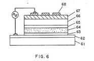
- Figs. 5 and 6 are sectional views showing, respectively, other exemplary embodiments of the thin film electroluminescent element according to this invention.
- a dielectric layer which has a composition generally expressed by AB 2 0 6 where A represents a divalent metal element, B represents a pentavalent metal element (and 0 represents oxygen) and which exhibits ey and E b of large values, to thereby allow the driving voltage to be lowered without decreasing brightness of the hitherto known thin film EL element.
- the voltage applied across the dielectric layer is represented by a product t i ⁇ E i , where t, represents the film thickness of the dielectric thin film and E i represents the electric field intensity applied to the dielectric thin film.
- the voltage.applied across the phosphor thin film becomes more effective as the value of t i ⁇ E i is smaller. It is safe to say that t, be in inverse proportion to E b of the dielectric thin film in order that the element can operate stably without undergoing the dielectric breakdown.
- E the electric field intensity E z in the phosphor thin film, the dielectric constant ⁇ Z of the phosphor thin film and ⁇ Y of the dielectric thin film
- E, E Z ⁇ Z / ⁇ Y
- E i is in inverse proportion to ⁇ Y , providing E z land ⁇ Z to be constant. Accordingly, it can be said that t i ⁇ E i is approximately in inverse proportion to the product of E b and ⁇ Y .
- the dielectric thin film is more advantageous with E b ⁇ Y of high value.
- the dielectric thin film expressed by the general formula of AB 2 0 6 and used according to the teaching of the present invention exhibits E b ⁇ E Y of a greater value than that of the heretofore used material and is preferable as the dielectric thin film for the EL element.
- A represents a divalent metal element such as Pb, Sn, Zn, Cd, Ba, Sr, Ca and Mg
- B represents Ta or Nb.
- a bulk or mass of a compound of these elements exhibit ⁇ Y of a great value.
- ⁇ Y of PbNb 2 O 6 is 300
- PbTa 2 O 6 is 300
- Nb 2 0 6 is 1600.
- ⁇ Y of the same value as the bulk it is difficult to realize ⁇ Y of the same value as the bulk.
- ⁇ Y of a value not smaller than 40 can be easily realized in a thin film fabricated by a sputtering process.
- E b of the thin film is as high as 2 x 10 6 V/cm or more.
- the value of E b ⁇ Y of such thin film is not smaller than 80 x 10 6 V/cm.
- the thin film formed of the compound mentioned above is excellent over the material used heretofore such as, for example Y 2 0 3 , A1 3 0 3 and Si 3 N 4 whose values of E b ⁇ Y are about 50 ⁇ 10 6 V/cm, 30 x 10 6 V/cm and 70 x 10 6 V/cm, respectively.
- the compound expressed by general formula AB 2 0 6 Nb and Ta which are most stable in pentavalence are preferable as the element represented by B.
- the divalent elements represented by A, Sr, Ba and Pb are very preferable.
- PbTa 2 O 6 and PbNb 2 O 6 where the element represented by A is Pb and whose values of E b ⁇ Y are 150 ⁇ 10 6 V/cm and 120 ⁇ 10 6 V/cm, respectively, provide very excellent thin film materials for the EL element.
- the thin film is formed by an RF sputtering method with a ceramic being used as a target. As the temperature of the substrate on which the thin film is to be formed is higher, the value of ⁇ Y of the thin film as formed becomes correspondingly greater.
- the dielectric breakdown field intensity E b assumes a substantially constant value when the temperature of the substrate is lower than about 400°C and is gradually decreased when the substrate temperature is elevated to a higher temperature.
- E b ⁇ Y becomes greatest when the temperature of substrate is approximately at 400°C. In the range of temperature mentioned . above, no adverse influence will be exerted to the phosphor thin film. Besides, glass may be used as the material for the substrate without giving rise to a problem such as thermal deformation of the substrate. Moreover, no turbidity in white will be produced due to the growth of particles.
- the thin film will be found to be amorphous when investigated by means of X-ray diffraction. Through chemical analysis and phosphor X-ray analysis, it has been ascertained that the thin film has a composition substantially coinciding with the general formula of AB 2 0 6 .
- the dielectric breakdown may generally be classified into two types.
- One is the dielectric breakdown of self-healing type. More specifically, referring to Fig. 1, an upper electrode 15 overlying a location 16 where the dielectric breakdown has occured is eliminated away under an area of several ten pm under discharging energy, wherein the upper electrode 15 is disconnected from a lower electrode 12.
- the dielectric breakdown occurring in the dielectric thin film of the composition expressed by the general formula AB 2 0 6 where A represents a divalent metal element and B represents a pentavalent metal element is of this type.
- a numeral 11 denotes a substrate, and 13 denotes a dielectric thin film.
- the other is the dielectric breakdown of the non self-healing type. As is shown in Fig.
- the upper electrode 25 is eliminated away only to such a small degree that the upper electrode 25 is electrically short-circuited to the lower electrode 22 through a hole 26 formed by the dielectric breakdown.
- the dielectric breakdown may spread over the whole dielectric film.
- the dielectric thin film containing perovskite type titanate as a main component belongs to this type.
- the electrode should have a thickness of several tens nm at minimum. Electrode material such as Au, Zn, AI and others is most likely to undergo the dielectric breakdown of the self-healing type. However, there exist some dielectric thin film in which no dielectric breakdown of the self-healing type takes place even with the electrode of Au, Zn, AI or the like in thickness of several tens nm. This dielectric breakdown is ascribable to the inherent nature of the material.
- the dielectric thin film whose dielectric breakdown is of the self-healing type is used as the dielectric thin film formed on the phosphor layer of the AC-driven thin film EL element, the dielectric breakdown occurring at the defective portion is of the first mentioned type.
- the material of the upper electrode is eliminated away over an area of several tens ⁇ m. Since an eliminated pinhole can not be visibly recognized, the dielectric breakdown of the self-healing type presents no practical problem.
- the dielectric thin film of the composition expressed by the general formula of AB 2 0 6 (where A represents a divalent metal element and B represents a pentavalent metal element) is susceptible to the dielectric breakdown of this type, it is preferred as the dielectric thin film for the AC-driven thin film EL element also in respect to the dielectric breakdown.
- the dielectric film whose dielectric breakdown is not of the self-healing type is formed on the phosphor layer of the AC-driven thin film EL element, the dielectric breakdown occurring at the defective portion is of the second mentioned type. The dielectric breakdown is likely to spread over the whole pixels, producing a visible deficiency. In the case of an X-Y matrix array, a line defect will be resulted.
- the thin film of perovskite type titanate can be easily fabricated with a large value of ⁇ Y and exhibit E b of a large value at the locations where no defects due to the pinholes and dusts are present, this film is insusceptible to the dielectric breakdown of the self-healing type.
- the thin film of strontium titanate or barium titanate having Sy of a great value the dielectric breakdown of the self-healing type is difficult to occur, these thin films were not used for the AC-driven thin film EL element.
- the dielectric thin film of the composition expressed by the general formula of AB 2 0 6 mentioned before is formed on the thin film of the above mentioned type, the dielectric breakdown occurring due to the pinholes and dusts is of the self-healing nature, to an advantage.
- Fig. 3 shows the example for comparison
- Fig. 4 shows an exemplary embodiment of the present invention.
- Y 2 0 3 -films 33 and 43 each of 40 nm in thickness were formed by an electron beam evaporating method on glass substrates 31 and 41 deposited with transparent electrodes 32 and 42 of ITO (indium tin oxide), respectively.
- phosphor layers 34 and 44 of ZnS:Mn were formed through simultaneous evaporation of ZnS and Mn. Film thickness is 600 nm. Heat treatment was carried out at 580°C in vacuum for one hour.
- the element was divided into five elements one 1 of which was used as a specimen for comparison and a Y 2 0 3 -film 35 of 400 nm thick was formed, as is shown in Fig. 3.
- the element 2 was formed with a Ta 2 0 5 -film 45 of 30 nm in thickness for the protection of ZnS:Mn by an electron beam evaporating method, as is shown in Fig. 4, in accordance with an embodiment of the present invention.
- a film 46 of PbNb 2 0 6 was formed through magnetron RF sputtering by using a ceramic of PbNb 2 0 6 as a target.
- the atmosphere for the sputtering contains O2 and Ar at the ratio of 1:4 at a pressure of 0.6 Pa.
- the temperature of the substrate is 420°C and the film thickness is 700 nm.
- the element 3 was formed with a film of PbTa 2 0 6 in thickness of 700 nm on the same conditions as in the case of the element 2 except that a target of PbTa 2 0 6 was employed in place of PbNb 2 0 6 .
- the element 4 was formed with a film of BaTa 2 0 6 in thickness of 500 nm on the same conditions as in the case of the element 2 except that BaTa 2 0 6 was used in place of PbNb 2 0 6 as the target.
- the element 5 was formed with a film of SrTa 2 0 6 in thickness of 450 nm on the same conditions as in the case of the element 2 except that SrTa 2 0 6 was used in place of PbNb 2 0 6 as the target.
- the PbNb 2 0 6 -film, the PbTa 2 0 6 -film, the BaTa 2 0 6 -film and the SrTa 2 0 6 -film fabricated on the aforementioned conditions have characteristically E b of 2.2 x 10 6 V/cm, 2.6 x 10 6 V/cm, 5.1 x 10 6 V/cm and 5.6 x 10 6 V/cm, respectively, and ey of 70, 48, 27 and 25, respectively.
- thin films of AI were deposited through vaporization to form light reflecting electrodes 36 and 47.
- Each of the EL elements fabricated in the manner described above was driven by applying a sine wave voltage of a frequency of 5 KHz across the electrodes.
- the voltage at which brightness was substantially saturated in the stable state was 150 V in the case of the element 1, 100 V in the case of the element 2, 110 V in the case of the element 3, 125 V in the case of the element 4 and 125 V in the case of the element 5.
- the saturated brightness was about 3000 cd/ M 2 in all of the five elements.
- a ZnO-film 53 having a thickness of 50 nm was formed by a sputtering method on a glass substrate 51 deposited with a transparent electrode 52 of ITO.
- the film 53 of ZnO has a resistivity of 8 x 10- 3 ⁇ cm and serves as a second electrode layer for preventing diffusion of In and Sn into ZnS from the transparent electrode 52 of ITO.
- the temperature of the substrate is 320°C; film thickness is 500 nm.
- the film 56 of PbNb 2 0 6 fabricated on the conditions mentioned above has characteristically E b of 2.5 x 10 6 V/cm and ⁇ Y of 56.
- the EL element manufactured in the manner described above was driven by applying a sine wave voltage of 5 KHz between the electrodes. Brightness was substantially saturated at about 70 V. In the stable state, brightness was 1900 cd /m 2 .
- a glass substrate 61 having a transparent electrode 62 of ITO was deposited with a Y 1 0 3 -film 63 in thickness of 40 nm through electron beam evaporation.
- a phosphor layer of 64 of ZnS:Mn was formed in thickness of 1.0 ⁇ m by simultaneously evaporating ZnS and Mn through vacuum vapor deposition. Heat treatment was conducted at 580°C in vacuum for an hour. Thereafter, a Ta 2 0 5 - film 65 is deposited in thickness of 40 nm through electron beam evaporation for protecting the film of ZnS:Mn.
- the element is divided into two, one of which was deposited with a SrTi0 3 -film in thickness of 1.4 pm while the other was deposited with a BaTi0 3 -film in thickness of 1.6 pm by a magnetron RF sputtering method.
- a mixed gas of 0 2 and Ar was used as the sputtering gas at pressure of 8 x 10 -1 Pa.
- the temperature of the substrate at that time is 420°C.
- a PbNb 2 0 6 -film 67 was deposited in thickness of 0.4 ⁇ m by a magnetron RF sputtering method.
- a mixed gas containing 0 2 and Ar at the ratio of 1 to 1 was used as the sputtering gas at a pressure of 0.6 Pa.
- a sintered body of PbNb 2 0 6 was used as the target.
- the temperature of the substrate is 380°C.
- a film 68 of AI was deposited in thickness of 70 nm to form the upper electrode.
- a voltage was applied between the electrodes of the thin film EL element thus manufactured and the applied voltage was progressively increased.
- dielectric breakdowns were all of the self-healing type. The number of the breakdowns was 0.5/cm 2 in both elements.
- the brightness was about 700 cd/ M 2 .
- the thin film electroluminescent element according to the invention can be operated stably with a low driving voltage.
Landscapes
- Chemical & Material Sciences (AREA)
- Engineering & Computer Science (AREA)
- Ceramic Engineering (AREA)
- Inorganic Chemistry (AREA)
- Electroluminescent Light Sources (AREA)
Abstract
Claims (8)
Applications Claiming Priority (4)
| Application Number | Priority Date | Filing Date | Title |
|---|---|---|---|
| JP91594/82 | 1982-05-28 | ||
| JP57091594A JPS58209093A (ja) | 1982-05-28 | 1982-05-28 | 薄膜発光素子 |
| JP57095430A JPS58212119A (ja) | 1982-06-03 | 1982-06-03 | 複合誘電体 |
| JP95430/82 | 1982-06-03 |
Publications (3)
| Publication Number | Publication Date |
|---|---|
| EP0111568A1 EP0111568A1 (fr) | 1984-06-27 |
| EP0111568A4 EP0111568A4 (fr) | 1984-09-28 |
| EP0111568B1 true EP0111568B1 (fr) | 1986-10-15 |
Family
ID=26433042
Family Applications (1)
| Application Number | Title | Priority Date | Filing Date |
|---|---|---|---|
| EP83901629A Expired EP0111568B1 (fr) | 1982-05-28 | 1983-05-26 | Dispositif electroluminescent a champ electrique a film mince |
Country Status (4)
| Country | Link |
|---|---|
| US (1) | US4547703A (fr) |
| EP (1) | EP0111568B1 (fr) |
| DE (1) | DE3367039D1 (fr) |
| WO (1) | WO1983004339A1 (fr) |
Cited By (1)
| Publication number | Priority date | Publication date | Assignee | Title |
|---|---|---|---|---|
| US7427422B2 (en) | 1999-05-14 | 2008-09-23 | Ifire Technology Corp. | Method of forming a thick film dielectric layer in an electroluminescent laminate |
Families Citing this family (22)
| Publication number | Priority date | Publication date | Assignee | Title |
|---|---|---|---|---|
| JPS60124396A (ja) * | 1983-12-09 | 1985-07-03 | 松下電器産業株式会社 | 薄膜発光素子 |
| JPS60182692A (ja) * | 1984-02-29 | 1985-09-18 | ホ−ヤ株式会社 | 薄膜el素子とその製造方法 |
| JPH086086B2 (ja) * | 1985-09-30 | 1996-01-24 | 株式会社リコー | 白色エレクトロルミネツセンス素子 |
| US4727004A (en) * | 1985-11-21 | 1988-02-23 | Sharp Kabushiki Kaisha | Thin film electroluminescent device |
| US4631633A (en) * | 1985-12-23 | 1986-12-23 | North American Philips Corporation | Thin film capacitors and method of making the same |
| JPH0697704B2 (ja) * | 1986-01-27 | 1994-11-30 | シャープ株式会社 | MIS型ZnS青色発光素子 |
| JPS63184287A (ja) * | 1986-09-25 | 1988-07-29 | 株式会社日立製作所 | 薄膜el素子及びその製造方法 |
| JPS63276895A (ja) * | 1987-05-08 | 1988-11-15 | Hitachi Ltd | エレクトロルミネセント素子の製造方法 |
| US4897319A (en) * | 1988-07-19 | 1990-01-30 | Planar Systems, Inc. | TFEL device having multiple layer insulators |
| DE68928245T2 (de) * | 1988-12-27 | 1997-12-11 | Canon Kk | Durch elektrisches Feld lichtemittierende Vorrichtung |
| US5432015A (en) * | 1992-05-08 | 1995-07-11 | Westaim Technologies, Inc. | Electroluminescent laminate with thick film dielectric |
| US5434013A (en) * | 1993-10-29 | 1995-07-18 | Fernandez; Robert | Low voltage illuminated automobile trim |
| JPH10308283A (ja) | 1997-03-04 | 1998-11-17 | Denso Corp | El素子およびその製造方法 |
| US6639355B1 (en) * | 1999-12-20 | 2003-10-28 | Morgan Adhesives Company | Multidirectional electroluminescent lamp structures |
| US6621212B1 (en) * | 1999-12-20 | 2003-09-16 | Morgan Adhesives Company | Electroluminescent lamp structure |
| JP3479273B2 (ja) * | 2000-09-21 | 2003-12-15 | Tdk株式会社 | 蛍光体薄膜その製造方法およびelパネル |
| JP2002110344A (ja) * | 2000-09-29 | 2002-04-12 | Tdk Corp | 薄膜el素子及びその製造方法 |
| US6793962B2 (en) * | 2000-11-17 | 2004-09-21 | Tdk Corporation | EL phosphor multilayer thin film and EL device |
| JP4171908B2 (ja) * | 2004-01-20 | 2008-10-29 | セイコーエプソン株式会社 | 強誘電体膜、強誘電体メモリ、及び圧電素子 |
| KR100850780B1 (ko) * | 2007-05-22 | 2008-08-06 | 삼성전기주식회사 | 질화물계 반도체 발광소자의 제조방법 |
| FR2988328B1 (fr) * | 2012-03-23 | 2014-12-19 | Bic Soc | Dispositif d'application de fluide et ses utilisations |
| WO2015119113A1 (fr) * | 2014-02-04 | 2015-08-13 | 日本碍子株式会社 | Corps stratifié, dispositif stratifié, et procédé de fabrication de ceux-ci |
Family Cites Families (13)
| Publication number | Priority date | Publication date | Assignee | Title |
|---|---|---|---|---|
| GB798503A (en) * | 1953-12-09 | 1958-07-23 | Thorn Electrical Ind Ltd | Improvements in and relating to electroluminescent lamps |
| US2731419A (en) * | 1954-08-12 | 1956-01-17 | Gen Electric | Ferroelectric ceramic composition |
| US3054919A (en) * | 1959-12-24 | 1962-09-18 | Westinghouse Electric Corp | Method of improving electroluminescent phosphor and electroluminescent device |
| US3129108A (en) * | 1960-12-23 | 1964-04-14 | Corning Glass Works | Electroluminescent cell and method |
| FR1409956A (fr) * | 1964-08-04 | 1965-09-03 | Corning Glass Works | Corps semi-cristallins en feuilles formant un support diélectrique |
| US4121941A (en) * | 1977-11-10 | 1978-10-24 | Matsushita Electric Industrial Co., Ltd. | Low microwave loss ceramics and method of manufacturing the same |
| US4132919A (en) * | 1977-12-12 | 1979-01-02 | Lockheed Missiles & Space Company, Inc. | Absorbing inhomogeneous film for high contrast display devices |
| JPS5510447A (en) * | 1978-07-07 | 1980-01-24 | Nippon Electric Co | Oxide permittivity material |
| US4225653A (en) * | 1979-03-26 | 1980-09-30 | E. I. Du Pont De Nemours And Company | X-ray intensifying screen based on rare earth tantalate |
| JPS5849995B2 (ja) * | 1979-09-20 | 1983-11-08 | 富士通株式会社 | El表示装置 |
| JPS5735891A (fr) * | 1980-08-14 | 1982-02-26 | Nippon Electric Co | |
| FI61983C (fi) * | 1981-02-23 | 1982-10-11 | Lohja Ab Oy | Tunnfilm-elektroluminensstruktur |
| US4387141A (en) * | 1982-05-12 | 1983-06-07 | E. I. Du Pont De Nemours And Company | X-Ray screens based on phosphor mixtures of CaWO4 and rare earth tantalates |
-
1983
- 1983-05-26 DE DE8383901629T patent/DE3367039D1/de not_active Expired
- 1983-05-26 EP EP83901629A patent/EP0111568B1/fr not_active Expired
- 1983-05-26 WO PCT/JP1983/000164 patent/WO1983004339A1/fr not_active Ceased
- 1983-05-26 US US06/576,394 patent/US4547703A/en not_active Expired - Lifetime
Cited By (1)
| Publication number | Priority date | Publication date | Assignee | Title |
|---|---|---|---|---|
| US7427422B2 (en) | 1999-05-14 | 2008-09-23 | Ifire Technology Corp. | Method of forming a thick film dielectric layer in an electroluminescent laminate |
Also Published As
| Publication number | Publication date |
|---|---|
| EP0111568A1 (fr) | 1984-06-27 |
| DE3367039D1 (en) | 1986-11-20 |
| EP0111568A4 (fr) | 1984-09-28 |
| US4547703A (en) | 1985-10-15 |
| WO1983004339A1 (fr) | 1983-12-08 |
Similar Documents
| Publication | Publication Date | Title |
|---|---|---|
| EP0111568B1 (fr) | Dispositif electroluminescent a champ electrique a film mince | |
| EP1352545B1 (fr) | Couche d'insertion pour afficheurs electroluminescents a film mince | |
| US6403204B1 (en) | Oxide phosphor electroluminescent laminate | |
| US20050236984A1 (en) | Light-emitting device and display device | |
| US20040170864A1 (en) | Aluminum nitride passivated phosphors for electroluminescent displays | |
| JPS60124396A (ja) | 薄膜発光素子 | |
| US20030039813A1 (en) | High performance dielectric layer and application to thin film electroluminescent devices | |
| JPH0744072B2 (ja) | El素子とその製造方法 | |
| JPH06310279A (ja) | エレクトロルミネセンスランプ | |
| CA1242021A (fr) | Element electroluminescent en couche mince | |
| KR100247141B1 (ko) | 전기장 발광소자 및 그 제조방법 | |
| JPH0740515B2 (ja) | 薄膜発光素子 | |
| JPH0632308B2 (ja) | 薄膜エレクトロルミネセンス素子およびその製造方法 | |
| JPH0118563B2 (fr) | ||
| JPH0516158B2 (fr) | ||
| JPH0439200B2 (fr) | ||
| JPH03112089A (ja) | 薄膜el素子 | |
| JPS59228397A (ja) | 薄膜発光素子 | |
| JPS6366895A (ja) | 薄膜el素子のエ−ジング方法 | |
| JPH01286290A (ja) | 交流駆動エレクトロルミネッセント・デバイス | |
| JPS6147096A (ja) | 薄膜el素子の製造方法 | |
| JPH0130279B2 (fr) | ||
| JPS6314833B2 (fr) | ||
| JPH0634389B2 (ja) | 薄膜発光素子の製造法 | |
| JPS6151797A (ja) | 薄膜el素子 |
Legal Events
| Date | Code | Title | Description |
|---|---|---|---|
| PUAI | Public reference made under article 153(3) epc to a published international application that has entered the european phase |
Free format text: ORIGINAL CODE: 0009012 |
|
| 17P | Request for examination filed |
Effective date: 19840215 |
|
| AK | Designated contracting states |
Designated state(s): DE FR GB |
|
| GRAA | (expected) grant |
Free format text: ORIGINAL CODE: 0009210 |
|
| AK | Designated contracting states |
Kind code of ref document: B1 Designated state(s): DE FR GB |
|
| REF | Corresponds to: |
Ref document number: 3367039 Country of ref document: DE Date of ref document: 19861120 |
|
| ET | Fr: translation filed | ||
| PLBE | No opposition filed within time limit |
Free format text: ORIGINAL CODE: 0009261 |
|
| STAA | Information on the status of an ep patent application or granted ep patent |
Free format text: STATUS: NO OPPOSITION FILED WITHIN TIME LIMIT |
|
| 26N | No opposition filed | ||
| REG | Reference to a national code |
Ref country code: GB Ref legal event code: 746 Effective date: 19951123 |
|
| REG | Reference to a national code |
Ref country code: FR Ref legal event code: D6 |
|
| PGFP | Annual fee paid to national office [announced via postgrant information from national office to epo] |
Ref country code: FR Payment date: 19970513 Year of fee payment: 15 |
|
| PGFP | Annual fee paid to national office [announced via postgrant information from national office to epo] |
Ref country code: GB Payment date: 19970519 Year of fee payment: 15 |
|
| PGFP | Annual fee paid to national office [announced via postgrant information from national office to epo] |
Ref country code: DE Payment date: 19970530 Year of fee payment: 15 |
|
| PG25 | Lapsed in a contracting state [announced via postgrant information from national office to epo] |
Ref country code: GB Free format text: LAPSE BECAUSE OF NON-PAYMENT OF DUE FEES Effective date: 19980526 |
|
| PG25 | Lapsed in a contracting state [announced via postgrant information from national office to epo] |
Ref country code: FR Free format text: LAPSE BECAUSE OF NON-PAYMENT OF DUE FEES Effective date: 19980531 |
|
| GBPC | Gb: european patent ceased through non-payment of renewal fee |
Effective date: 19980526 |
|
| PG25 | Lapsed in a contracting state [announced via postgrant information from national office to epo] |
Ref country code: DE Free format text: LAPSE BECAUSE OF NON-PAYMENT OF DUE FEES Effective date: 19990302 |
|
| REG | Reference to a national code |
Ref country code: FR Ref legal event code: ST |