EP0112695B1 - Verfahren zur Herstellung eines mehrfach gefärbten Bauteiles - Google Patents
Verfahren zur Herstellung eines mehrfach gefärbten Bauteiles Download PDFInfo
- Publication number
- EP0112695B1 EP0112695B1 EP83307643A EP83307643A EP0112695B1 EP 0112695 B1 EP0112695 B1 EP 0112695B1 EP 83307643 A EP83307643 A EP 83307643A EP 83307643 A EP83307643 A EP 83307643A EP 0112695 B1 EP0112695 B1 EP 0112695B1
- Authority
- EP
- European Patent Office
- Prior art keywords
- film
- transparent
- aluminium
- strips
- colour
- Prior art date
- Legal status (The legal status is an assumption and is not a legal conclusion. Google has not performed a legal analysis and makes no representation as to the accuracy of the status listed.)
- Expired
Links
Images

Classifications
-
- G—PHYSICS
- G02—OPTICS
- G02F—OPTICAL DEVICES OR ARRANGEMENTS FOR THE CONTROL OF LIGHT BY MODIFICATION OF THE OPTICAL PROPERTIES OF THE MEDIA OF THE ELEMENTS INVOLVED THEREIN; NON-LINEAR OPTICS; FREQUENCY-CHANGING OF LIGHT; OPTICAL LOGIC ELEMENTS; OPTICAL ANALOGUE/DIGITAL CONVERTERS
- G02F1/00—Devices or arrangements for the control of the intensity, colour, phase, polarisation or direction of light arriving from an independent light source, e.g. switching, gating or modulating; Non-linear optics
- G02F1/01—Devices or arrangements for the control of the intensity, colour, phase, polarisation or direction of light arriving from an independent light source, e.g. switching, gating or modulating; Non-linear optics for the control of the intensity, phase, polarisation or colour
- G02F1/13—Devices or arrangements for the control of the intensity, colour, phase, polarisation or direction of light arriving from an independent light source, e.g. switching, gating or modulating; Non-linear optics for the control of the intensity, phase, polarisation or colour based on liquid crystals, e.g. single liquid crystal display cells
- G02F1/133—Constructional arrangements; Operation of liquid crystal cells; Circuit arrangements
- G02F1/1333—Constructional arrangements; Manufacturing methods
- G02F1/1335—Structural association of cells with optical devices, e.g. polarisers or reflectors
- G02F1/133509—Filters, e.g. light shielding masks
- G02F1/133514—Colour filters
- G02F1/133516—Methods for their manufacture, e.g. printing, electro-deposition or photolithography
-
- C—CHEMISTRY; METALLURGY
- C25—ELECTROLYTIC OR ELECTROPHORETIC PROCESSES; APPARATUS THEREFOR
- C25D—PROCESSES FOR THE ELECTROLYTIC OR ELECTROPHORETIC PRODUCTION OF COATINGS; ELECTROFORMING; APPARATUS THEREFOR
- C25D11/00—Electrolytic coating by surface reaction, i.e. forming conversion layers
- C25D11/02—Anodisation
- C25D11/04—Anodisation of aluminium or alloys based thereon
-
- C—CHEMISTRY; METALLURGY
- C25—ELECTROLYTIC OR ELECTROPHORETIC PROCESSES; APPARATUS THEREFOR
- C25D—PROCESSES FOR THE ELECTROLYTIC OR ELECTROPHORETIC PRODUCTION OF COATINGS; ELECTROFORMING; APPARATUS THEREFOR
- C25D11/00—Electrolytic coating by surface reaction, i.e. forming conversion layers
- C25D11/02—Anodisation
- C25D11/04—Anodisation of aluminium or alloys based thereon
- C25D11/18—After-treatment, e.g. pore-sealing
- C25D11/24—Chemical after-treatment
- C25D11/246—Chemical after-treatment for sealing layers
-
- G—PHYSICS
- G02—OPTICS
- G02F—OPTICAL DEVICES OR ARRANGEMENTS FOR THE CONTROL OF LIGHT BY MODIFICATION OF THE OPTICAL PROPERTIES OF THE MEDIA OF THE ELEMENTS INVOLVED THEREIN; NON-LINEAR OPTICS; FREQUENCY-CHANGING OF LIGHT; OPTICAL LOGIC ELEMENTS; OPTICAL ANALOGUE/DIGITAL CONVERTERS
- G02F1/00—Devices or arrangements for the control of the intensity, colour, phase, polarisation or direction of light arriving from an independent light source, e.g. switching, gating or modulating; Non-linear optics
- G02F1/01—Devices or arrangements for the control of the intensity, colour, phase, polarisation or direction of light arriving from an independent light source, e.g. switching, gating or modulating; Non-linear optics for the control of the intensity, phase, polarisation or colour
- G02F1/15—Devices or arrangements for the control of the intensity, colour, phase, polarisation or direction of light arriving from an independent light source, e.g. switching, gating or modulating; Non-linear optics for the control of the intensity, phase, polarisation or colour based on an electrochromic effect
- G02F1/153—Constructional details
- G02F1/1533—Constructional details structural features not otherwise provided for
-
- B—PERFORMING OPERATIONS; TRANSPORTING
- B41—PRINTING; LINING MACHINES; TYPEWRITERS; STAMPS
- B41M—PRINTING, DUPLICATING, MARKING, OR COPYING PROCESSES; COLOUR PRINTING
- B41M5/00—Duplicating or marking methods; Sheet materials for use therein
- B41M5/025—Duplicating or marking methods; Sheet materials for use therein by transferring ink from the master sheet
- B41M5/035—Duplicating or marking methods; Sheet materials for use therein by transferring ink from the master sheet by sublimation or volatilisation of pre-printed design, e.g. sublistatic
- B41M5/0351—Duplicating or marking methods; Sheet materials for use therein by transferring ink from the master sheet by sublimation or volatilisation of pre-printed design, e.g. sublistatic on anodized aluminium
Definitions
- the present invention relates to a method for making a multicoloured member such for example, as a plate, a colour filter, or a display device.
- One known method for manufacturing a multi- coloured plate is known as "staining” and includes utilizing surface diffusion of metal ions.
- Other known methods comprise printing by burning on low melting temperature glass frit, and employing a printing ink containing an organic polymeric binder.
- a coloured plate by forming a thin film of aluminium on a base plate, anodically oxidising this thin film, colouring the thin film of anodically oxidized aluminium by the use of organic or inorganic colouring material, and thereafter sealing the porosity on the surface of the anodically oxidized aluminium thin film so as to stabilize the coloured layer.
- US-A-3,619,385 discloses the provision of a transparent oxide film dissimilar thickness at different film areas so that these areas appear to be differently coloured due to light interference phenomena.
- EP-A-0,014,035 discloses the anodic oxidation of an aluminium article so as to provide the article with a corrosion-resistant surface. Such anodic oxidation produces a surface which can be dyed provided it has not been subjected to boiling water, pressurised steam or other de-activating treatment.
- a method of making a multi- coloured member comprising arranging that a surface of the member cannot normally be dyed, treating a portion only of said surface so that it is rendered capable of being dyed, dyeing the said portion a predetermined colour and subjecting the dyed portion to a further treatment which prevents further dyeing thereof, at least one further portion of the surface being subsequently so treated, dyed a different colour, and subjected to the further treatment, characterised by forming a transparent electrode film on the entire surface of a transparent glass substrate and by forming an aluminium film having a uniform thickness on the entire surface of said transparent electrode film, etching said aluminium film and said transparent electrode film identically to form a plurality of separate patterned parts, anodically oxidizing completely a first patterned part of said aluminium film to form said first part into a transparent oxidized aluminium film having a uniform thickness, colouring said transparent oxidized aluminium first part a first colour, sealing the porosity of the surface of said
- the plurality of separate patterned parts comprises three parts.
- the said three parts may be coloured red, green and blue respectively.
- the thickness of the said aluminium film may be 1 to 2 J-lm.
- Figure 1 shows an example of a known multi- colour display device or cell using a colour filter.
- Numeral 1 is a transparent substrate; 2 are transparent electrodes on each of which a desired figure or a letter is pattened; 3 is a colour filter having portions 3a, 3b, 3c each of which is provided with a respective transparent electrode 2; 4 is a second transparent electrode; and 5 is a counter substrate.
- a display material (not shown) which acts as an optical shutter, such as liquid crystal material electrochromic material or the like, is sandwiched and held between the transparent substrate 1 and the counter substrate 5.
- the optical shutter on the red portions 3a and on the green portions 3b "open", and the optical shutter on the blue portions 3c "closes".
- yellow is displayed by additive colour mixture.
- the colour filter 3 has an appropriate light transparency and the counter substrate 5 is transparent, a similar effect is obtained if a luminous display material is sandwiched and held between the transparent substrate 1 and the counter substrate 5 and viewed from the direction of the counter substrate 5.
- the colour filters can be formed by means of screen printing, photo-lithography or the like.
- screen printing however, a pattern cannot be made sufficiently fine. That is to say, the more the pattern is multicoloured, the worse is the precision of the printing, and colour shear occurs.
- photo-lithography the pattern can be very small, but manufacture is extremely complicated since a photo-lithography step is needed for each colour change. This is inconsistent with the advantages ofcolourfilters, namely simplicity and capability of providing a multicolour display.
- the present invention therefore aims to overcome the above-mentioned drawbacks. It is thus an object of the present invention to provide a method for manufacturing a multi-coloured member having a highly accurate and easily fabricated pattern at low cost.
- the method of making a multi-coloured member according to the present invention may be carried out in outline as follows.
- Substantially the whole of one surface of a base plate is provided by spattering or vacuum evaporation with a plurality of aluminium films or with a single such film which is subsequently divided into a plurality of films.
- the aluminium film or films is then dry-etched or chemically etched into a desired plurality of patterns as shown at 3a, 3b, 3c in Figure 1.
- a part of the so-formed plurality of patterns is selectively connected to the terminal of a power source (not shown) so as to anodically oxidize the part in an anodically oxidizing bath.
- This oxidized aluminium film has quite considerable transparency for visible rays.
- This oxidized aluminium film is also capable of being coloured by various methods. Therefore, it is possible to colour only the oxidized aluminium film, while the other aluminium films, or the rest of the single aluminium film, is left uncoloured.
- a method for easily manufacturing multi-coloured film is obtained by repeating these selective oxidation processes and colouring processes. This method does not involve any complicated processes such as are employed in a photo-resist method. This method also does not suffer from the drawback which exists when a sublimate dye is used, namelythat it is very hard to obtain a very fine pattern.
- a multicoloured plate having high accuracy can easily be obtained regardless of the shades of colour employed and the fineness of the pattern.
- the present invention involves the anodic oxidation of aluminium.
- an AI film is coated over the whole surface of a transparent electrode (Sn0 2 , ITO or the like) by spattering, vacuum evaporation or the like.
- the AI film and the transparent electrode may then be dry etched or chemically etched into a desired pattern, e.g. in strips.
- strips of transparent electrodes and strips of AI film may completely overlap each other.
- a patterned transparent electrode and its AI film may be selected as desired and conneced so as to be oxidized anodically in an anodic oxidation bath.
- only the AI film connected to the electrode will be changed to an aluminium oxide film.
- Aluminium oxide has extremely high transparency with respect to the viewed light and can be coloured by various methods.
- Method for manufacturing a multi-coloured filter The first process: Forming a transparent electrode.
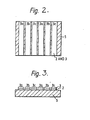
- a transparent electrode film 2 made of tin dioxide or indium tin oxide is first formed on the entire surface of a transparent glass substrate 5 ( Figures 2 and 3).
- the second process Forming aluminium film.
- An aluminium film 3 is formed on the transparent electrode film 2 to a thickness of 1 to 2 ⁇ m by spattering.
- the aluminium film 3 covers the entire surface of the transparent electrode film 2.
- the third process Etching a pattern.
- the aluminium film 3 and the transparent electrode film 2 are simultaneously identically etched by dry-etching or chemical etching to form a strip pattern.
- the width of a single strip is 50 ⁇ m.
- the distance between two adjacent strips is 20 pm.
- the fourth process Anodic oxidation.
- the strips 3a are coloured red, the strips 3b are coloured green and the strips 3c are coloured blue. Then the first strips to be coloured are assumed to be the strips 3a. Only the strips 3a are first selected for anodic oxidation, the transparent electrode and the aluminium film of the strips 3a being connected to the electrode of a power source (not shown).
- the filter is totally immersed in a 15 weight % sulphuric acid aqueous solution bath together with a platinum plate having a larger surface than the strip surface of the aluminium film, the platinum plate serving as a cathode.
- the aluminium strips 3a are anodically oxidized by applying a constant voltage ranging between +4.0 volts and +5.0 volts at room temperature.
- All of the aluminium film on the strips 3a is changed to a transparent oxidized aluminium film. It takes about 30 minutes or 60 minutes depending on the thickness of the aluminium film to finish the anodic oxidation and to change the aluminium film on the strips 3a to a transparent oxidized aluminium film. Thus the strips 3a alone become transparent while other strips 3b and 3c are left as opaque parts of the aluminium film.
- the fifth process Colouring the strips 3a red.
- the transparent glass substrate 5 on which the selectively oxidized aluminium film of the strips 3a is provided is totally immersed in an acid bath containing the red acid dye Alizarine Rubinol 3G for several minutes so that the transparent oxidized aluminium film formed on the surface of the strips 3a is coloured red.
- the sixth process Porosity-sealing treatment.
- the porosity on the oxidized aluminium film which is coloured red is sealed by subjecting the same to steam.
- the seventh process Colouring the strips 3b green.
- the aluminium film of the strip 3b is selectively anodically oxidized to be changed to a transparent oxidized aluminium film, which is immersed in an acid bath containing the green dye Aluminium Green GLW, and therefore is coloured green. After this the aluminium film which is coloured green is subjected to a porosity-sealing treatment.
- the eighth process Colouring the strips 3c blue.
- the aluminium film of the strips 3c is selectively anodically oxidized to be changed to a transparent oxidized aluminium film, which is immersed in an acid bath containing the blue acid dye Aluminium Blue LLW, and therefore is coloured blue.
- the aluminium film which is coloured blue is subjected to a porosity-sealing treatment.
- a colour filter having red, green and blue strips is produced.
- the first process Forming an AI film.
- An AI film of 1-2 um thickness is formed over the whole surface of the transparent electrode 2 (Sn0 2 , ITO or the like) on the transparent glass substrate 5 ( Figure 4) by spattering.
- the AI film may alternatively be formed by vacuum evaporation.
- the second process Pattern etching.
- the AI film and the transparent electrode are dry etched or chemically etched into a strip pattern whose strips are 50 ⁇ m wide and spaced from each other by 20 um.
- the strips 3a, 3b and 3c are respectively coloured red, green and blue. If the colour to be initially coloured is red, for example, only the strips 3a are selected, and the transparent electrode and the AI film of the strips 3a are connected to the electrode of a power source (not shown). Then the anodic oxidation is carried out in a 15 weight % sulphuric acid solution using a Pt plate as a cathode having an area equivalent to or more than the anode AI film at room temperature and at a constant voltage of +4.0 volts to +5.0 volts, whereby the AI film on the transparent electrode becomes a transparent aluminium oxide film.
- the time taken to complete the anodic oxidation and change the AI film on the transparent electrode to a transparent oxide aluminium film is about 30-60. minutes though the time differs according to the thickness of the AI film. Thus, only the strips 3a are transparent, and the strips 3b and 3c are left as opaque AI films.
- a chromic acid anhydride bath, an oxalic acid bath, a phosphoric acid bath or the like can be used as the anodic oxidation bath.
- the transparent glass substrate which carries the AI film of the strips 3a thereon which have
- the fifth process Porosity-sealing treatment.
- the porosity of the anodic oxidation film of the red strips 3a is sealed in steam.
- the anodic oxidation film after colouration and porosity-sealing treatment is less easily bleached and cannot subsequently be another colour even after the AI film of the strips 3b and 3c are anodically oxidized and then coloured in the following processes. Further, the porosity-sealing treatment improves the chemical resistance, heat resistance, and light resistance of the filter, and the reliability in manufacturing the display device is also enhanced. In addition to using steam for the porosity-sealing treatment, satisfactory results can also be obtained by using sodium nickel acetate and boiling water for effecting porosity sealing.
- the seventh process Colouring the strips 3c blue.
- the eighth process Forming an alignment film.
- Alignment films 8 which are aligned with liquid crystal material 9, are formed by oblique evaporation of, for example, SiO on the strip colour filter of red, green and blue formed by means of the above processes and on the second electrode 4.
- the ninth process Assembling the liquid crystal display device.
- a TN-type liquid crystal display device which can easily display multicolour or full colour is completed as shown in Figure 4 by holding a nematic liquid crystal layer 9 between the colour filter and the second transparent electrode 4 on which an alignment film 8 is formed.
- the liquid crystal display device is characterized in that the transparent electrodes 2 of the anodically oxidized AI film of the strips 3a, 3b and 3c respectively are used as driving electrodes for the liquid crystal display device. Moreover, the strips 3a 3b and 3c of the completed colour filter respectively overlie the transparent electrodes 2 which act as driving electrodes.
- use may also be made of a diochroic colour pigment dissolved in G-H type material or DSM nematic liquid crystal material.
Landscapes
- Physics & Mathematics (AREA)
- Chemical & Material Sciences (AREA)
- Nonlinear Science (AREA)
- Engineering & Computer Science (AREA)
- Optics & Photonics (AREA)
- General Physics & Mathematics (AREA)
- Chemical Kinetics & Catalysis (AREA)
- Electrochemistry (AREA)
- Materials Engineering (AREA)
- Metallurgy (AREA)
- Organic Chemistry (AREA)
- Crystallography & Structural Chemistry (AREA)
- Mathematical Physics (AREA)
- Manufacturing & Machinery (AREA)
- General Chemical & Material Sciences (AREA)
- Liquid Crystal (AREA)
- Devices For Indicating Variable Information By Combining Individual Elements (AREA)
Claims (4)
Applications Claiming Priority (4)
| Application Number | Priority Date | Filing Date | Title |
|---|---|---|---|
| JP233931/82 | 1982-12-22 | ||
| JP57233932A JPS59114571A (ja) | 1982-12-22 | 1982-12-22 | 多色表示装置の製造方法 |
| JP233932/82 | 1982-12-22 | ||
| JP57233931A JPS59114508A (ja) | 1982-12-22 | 1982-12-22 | 多色表面着色体の製造方法 |
Publications (2)
| Publication Number | Publication Date |
|---|---|
| EP0112695A1 EP0112695A1 (de) | 1984-07-04 |
| EP0112695B1 true EP0112695B1 (de) | 1987-08-12 |
Family
ID=26531267
Family Applications (1)
| Application Number | Title | Priority Date | Filing Date |
|---|---|---|---|
| EP83307643A Expired EP0112695B1 (de) | 1982-12-22 | 1983-12-15 | Verfahren zur Herstellung eines mehrfach gefärbten Bauteiles |
Country Status (3)
| Country | Link |
|---|---|
| US (1) | US4528073A (de) |
| EP (1) | EP0112695B1 (de) |
| DE (1) | DE3372994D1 (de) |
Families Citing this family (13)
| Publication number | Priority date | Publication date | Assignee | Title |
|---|---|---|---|---|
| JPS60254001A (ja) * | 1984-05-14 | 1985-12-14 | Nissha Printing Co Ltd | カラ−フイルタ− |
| WO1987003381A1 (fr) * | 1985-11-28 | 1987-06-04 | Nissha Printing Co., Ltd. | Filtre couleur de haute precision possedant d'excellentes proprietes et procede de production |
| KR960013793B1 (ko) * | 1987-01-28 | 1996-10-10 | 니혼샤신인사츠 가부시키가이샤 | 컬러필터의 제조방법 |
| DE3718849A1 (de) * | 1987-06-05 | 1988-12-15 | Henkel Kgaa | Elektrolytisches einfaerben von anodisiertem aluminium |
| US4877697A (en) * | 1988-05-26 | 1989-10-31 | Hoechst Aktiengesellschaft | Color filter array for liquid crystal display device |
| WO1990016057A1 (en) * | 1989-06-17 | 1990-12-27 | Glick William F | Color display system using thin film color control |
| JP3199913B2 (ja) * | 1993-06-16 | 2001-08-20 | 株式会社半導体エネルギー研究所 | 液晶電気光学装置およびその作製方法 |
| US5835167A (en) * | 1994-12-21 | 1998-11-10 | Philips Electronics North America | Plasma addressed liquid crystal display with reduced column voltages |
| US5947369A (en) * | 1995-09-21 | 1999-09-07 | Temtec, Inc. | Electronic time badge |
| US20050270619A1 (en) * | 2002-07-26 | 2005-12-08 | Koninklijke Philips Electronics N.V. | Electrochromic color display having different electrochromic materials |
| CN104562129A (zh) * | 2013-10-17 | 2015-04-29 | 富鼎电子科技(嘉善)有限公司 | 金属基体表面处理方法 |
| CN105887155B (zh) * | 2016-05-27 | 2018-12-04 | 深圳天珑无线科技有限公司 | 一种铝合金表面双色阳极氧化方法 |
| CN110512257B (zh) * | 2019-08-02 | 2021-06-11 | 义乌市君胜科技有限公司 | 一种高耐热腐性涂层封孔剂 |
Citations (1)
| Publication number | Priority date | Publication date | Assignee | Title |
|---|---|---|---|---|
| EP0014035A1 (de) * | 1979-01-08 | 1980-08-06 | Honny Chemicals Co. Ltd. | Verfahren zur Oberflächenbehandlung von Aluminium-Gegenständen |
Family Cites Families (9)
| Publication number | Priority date | Publication date | Assignee | Title |
|---|---|---|---|---|
| US2424621A (en) * | 1945-07-06 | 1947-07-29 | Jr Marvin R Mcclatchey | Shipping tags, labels, or the like and method of making the same |
| US3284321A (en) * | 1962-07-19 | 1966-11-08 | Howard A Fromson | Manufacture of aluminum articles with anodized surfaces presenting multicolor effects |
| GB1174563A (en) * | 1966-02-26 | 1969-12-17 | Kenneth Edward Roberts | Production of Anodised Surfaces of Aluminium or Aluminium Alloys |
| US3450606A (en) * | 1966-03-17 | 1969-06-17 | Reynolds Metals Co | Multi-colored aluminum anodizing process |
| US3619385A (en) * | 1968-02-05 | 1971-11-09 | Nadezhda Vasilievna Rjumshina | Process for manufacturing an article with a polychrome picture imposed on the surface thereof |
| US3839163A (en) * | 1971-08-31 | 1974-10-01 | Riken Light Metal Ind Co | Process for forming on an aluminum surface a colored design |
| JPS5116242A (en) * | 1974-07-31 | 1976-02-09 | Nippon Light Metal Co | Aruminiumu moshikuha aruminiumugokinzaino chakushokusankahimakuseiseiho |
| JPS51107318A (en) * | 1975-03-18 | 1976-09-22 | Dainippon Printing Co Ltd | Hyomenchakushokutai oyobi sonoseizoho |
| DE3265804D1 (en) * | 1981-05-19 | 1985-10-03 | Sankyo Alu Ind | Method of treating a surface of an aluminum to form a pattern thereon |
-
1983
- 1983-12-15 EP EP83307643A patent/EP0112695B1/de not_active Expired
- 1983-12-15 DE DE8383307643T patent/DE3372994D1/de not_active Expired
- 1983-12-21 US US06/563,946 patent/US4528073A/en not_active Expired - Fee Related
Patent Citations (1)
| Publication number | Priority date | Publication date | Assignee | Title |
|---|---|---|---|---|
| EP0014035A1 (de) * | 1979-01-08 | 1980-08-06 | Honny Chemicals Co. Ltd. | Verfahren zur Oberflächenbehandlung von Aluminium-Gegenständen |
Non-Patent Citations (1)
| Title |
|---|
| Römpps Chemie-Lexikon 7th edition (1973) p. 1003. * |
Also Published As
| Publication number | Publication date |
|---|---|
| DE3372994D1 (en) | 1987-09-17 |
| US4528073A (en) | 1985-07-09 |
| EP0112695A1 (de) | 1984-07-04 |
Similar Documents
| Publication | Publication Date | Title |
|---|---|---|
| US4528073A (en) | Method for manufacturing multicolored plate, multicolored filter and multicolored display device | |
| US5177627A (en) | Electrode plate with conductive color filter | |
| DE69625052T2 (de) | Verfahren zur herstellung einer flüssigkristall-anzeige | |
| US20030099887A1 (en) | Color filters for liquid crystal display panels and method of producing the same | |
| DE3587215T2 (de) | Farbfilter. | |
| DE3237323C2 (de) | ||
| DE2643678A1 (de) | Verfahren zur herstellung einer elektrochromen anzeigevorrichtung | |
| KR930010664B1 (ko) | 액정표시장치의 제조방법 | |
| JPS60179703A (ja) | 多色表示装置の製造方法 | |
| EP0718644B1 (de) | Herstellungsverfahren für Farbfilter | |
| JPS62144194A (ja) | 液晶表示素子 | |
| RU2030775C1 (ru) | Способ изготовления многоцветного оптического фильтра для жидкокристаллического устройства | |
| JPS61281220A (ja) | カラ−フイルタの製造方法 | |
| JPS6377018A (ja) | 反射型カラ−液晶パネル | |
| JPS63155003A (ja) | 多色表示装置の製造方法 | |
| JPS63147104A (ja) | 多色表示装置の製造方法 | |
| JPS63146002A (ja) | 反射型カラ−フイルタの製造方法 | |
| JPS6223283B2 (de) | ||
| JPH0128927B2 (de) | ||
| JPS60221728A (ja) | 液晶表示器 | |
| JPH0128928B2 (de) | ||
| JPS63148201A (ja) | 反射型カラ−フイルタの製造方法 | |
| JPS6073524A (ja) | 液晶素子 | |
| JPS6258219A (ja) | カラ−液晶表示装置 | |
| JPH02129602A (ja) | カラーフィルターの製造方法 |
Legal Events
| Date | Code | Title | Description |
|---|---|---|---|
| PUAI | Public reference made under article 153(3) epc to a published international application that has entered the european phase |
Free format text: ORIGINAL CODE: 0009012 |
|
| AK | Designated contracting states |
Designated state(s): CH DE FR GB LI |
|
| 17P | Request for examination filed |
Effective date: 19841220 |
|
| GRAA | (expected) grant |
Free format text: ORIGINAL CODE: 0009210 |
|
| AK | Designated contracting states |
Kind code of ref document: B1 Designated state(s): CH DE FR GB LI |
|
| ET | Fr: translation filed | ||
| REF | Corresponds to: |
Ref document number: 3372994 Country of ref document: DE Date of ref document: 19870917 |
|
| RAP2 | Party data changed (patent owner data changed or rights of a patent transferred) |
Owner name: SEIKO INSTRUMENTS INC. |
|
| PLBE | No opposition filed within time limit |
Free format text: ORIGINAL CODE: 0009261 |
|
| STAA | Information on the status of an ep patent application or granted ep patent |
Free format text: STATUS: NO OPPOSITION FILED WITHIN TIME LIMIT |
|
| 26N | No opposition filed | ||
| REG | Reference to a national code |
Ref country code: GB Ref legal event code: 746 Effective date: 19940919 |
|
| PGFP | Annual fee paid to national office [announced via postgrant information from national office to epo] |
Ref country code: GB Payment date: 19951206 Year of fee payment: 13 |
|
| PGFP | Annual fee paid to national office [announced via postgrant information from national office to epo] |
Ref country code: FR Payment date: 19951212 Year of fee payment: 13 |
|
| PGFP | Annual fee paid to national office [announced via postgrant information from national office to epo] |
Ref country code: DE Payment date: 19951214 Year of fee payment: 13 |
|
| PGFP | Annual fee paid to national office [announced via postgrant information from national office to epo] |
Ref country code: CH Payment date: 19951229 Year of fee payment: 13 |
|
| REG | Reference to a national code |
Ref country code: FR Ref legal event code: D9 Free format text: CORRECTION |
|
| PG25 | Lapsed in a contracting state [announced via postgrant information from national office to epo] |
Ref country code: GB Effective date: 19961215 |
|
| PG25 | Lapsed in a contracting state [announced via postgrant information from national office to epo] |
Ref country code: LI Effective date: 19961231 Ref country code: CH Effective date: 19961231 |
|
| GBPC | Gb: european patent ceased through non-payment of renewal fee |
Effective date: 19961215 |
|
| REG | Reference to a national code |
Ref country code: CH Ref legal event code: PL |
|
| PG25 | Lapsed in a contracting state [announced via postgrant information from national office to epo] |
Ref country code: FR Effective date: 19970829 |
|
| PG25 | Lapsed in a contracting state [announced via postgrant information from national office to epo] |
Ref country code: DE Effective date: 19970902 |
|
| REG | Reference to a national code |
Ref country code: FR Ref legal event code: ST |