EP0115514B1 - Support de circuit integre - Google Patents
Support de circuit integre Download PDFInfo
- Publication number
- EP0115514B1 EP0115514B1 EP83902536A EP83902536A EP0115514B1 EP 0115514 B1 EP0115514 B1 EP 0115514B1 EP 83902536 A EP83902536 A EP 83902536A EP 83902536 A EP83902536 A EP 83902536A EP 0115514 B1 EP0115514 B1 EP 0115514B1
- Authority
- EP
- European Patent Office
- Prior art keywords
- contacts
- chip
- insulating material
- spacer
- chip carrier
- Prior art date
- Legal status (The legal status is an assumption and is not a legal conclusion. Google has not performed a legal analysis and makes no representation as to the accuracy of the status listed.)
- Expired
Links
Images



Classifications
-
- H—ELECTRICITY
- H10—SEMICONDUCTOR DEVICES; ELECTRIC SOLID-STATE DEVICES NOT OTHERWISE PROVIDED FOR
- H10W—GENERIC PACKAGES, INTERCONNECTIONS, CONNECTORS OR OTHER CONSTRUCTIONAL DETAILS OF DEVICES COVERED BY CLASS H10
- H10W70/00—Package substrates; Interposers; Redistribution layers [RDL]
- H10W70/60—Insulating or insulated package substrates; Interposers; Redistribution layers
- H10W70/62—Insulating or insulated package substrates; Interposers; Redistribution layers characterised by their interconnections
- H10W70/65—Shapes or dispositions of interconnections
- H10W70/657—Shapes or dispositions of interconnections on sidewalls or bottom surfaces of the package substrates, interposers or redistribution layers
-
- H—ELECTRICITY
- H10—SEMICONDUCTOR DEVICES; ELECTRIC SOLID-STATE DEVICES NOT OTHERWISE PROVIDED FOR
- H10W—GENERIC PACKAGES, INTERCONNECTIONS, CONNECTORS OR OTHER CONSTRUCTIONAL DETAILS OF DEVICES COVERED BY CLASS H10
- H10W70/00—Package substrates; Interposers; Redistribution layers [RDL]
- H10W70/60—Insulating or insulated package substrates; Interposers; Redistribution layers
- H10W70/611—Insulating or insulated package substrates; Interposers; Redistribution layers for connecting multiple chips together
-
- H—ELECTRICITY
- H10—SEMICONDUCTOR DEVICES; ELECTRIC SOLID-STATE DEVICES NOT OTHERWISE PROVIDED FOR
- H10W—GENERIC PACKAGES, INTERCONNECTIONS, CONNECTORS OR OTHER CONSTRUCTIONAL DETAILS OF DEVICES COVERED BY CLASS H10
- H10W90/00—Package configurations
- H10W90/401—Package configurations characterised by multiple insulating or insulated package substrates, interposers or RDLs
-
- H—ELECTRICITY
- H10—SEMICONDUCTOR DEVICES; ELECTRIC SOLID-STATE DEVICES NOT OTHERWISE PROVIDED FOR
- H10W—GENERIC PACKAGES, INTERCONNECTIONS, CONNECTORS OR OTHER CONSTRUCTIONAL DETAILS OF DEVICES COVERED BY CLASS H10
- H10W72/00—Interconnections or connectors in packages
- H10W72/071—Connecting or disconnecting
- H10W72/075—Connecting or disconnecting of bond wires
- H10W72/07551—Connecting or disconnecting of bond wires characterised by changes in properties of the bond wires during the connecting
- H10W72/07554—Connecting or disconnecting of bond wires characterised by changes in properties of the bond wires during the connecting changes in dispositions
-
- H—ELECTRICITY
- H10—SEMICONDUCTOR DEVICES; ELECTRIC SOLID-STATE DEVICES NOT OTHERWISE PROVIDED FOR
- H10W—GENERIC PACKAGES, INTERCONNECTIONS, CONNECTORS OR OTHER CONSTRUCTIONAL DETAILS OF DEVICES COVERED BY CLASS H10
- H10W72/00—Interconnections or connectors in packages
- H10W72/50—Bond wires
- H10W72/541—Dispositions of bond wires
- H10W72/547—Dispositions of multiple bond wires
Definitions
- the invention relates to chip carriers. More specifically, the invention relates to a chip carrier having external first and second major surfaces facing in opposite directions, comprising a body of electrically insulating material defining and separating the major surfaces and carrying a chip, electrical contacts arranged on an edge of the insulating material and electrical connections carried by the insulating material and connecting the contacts to the chip.
- Such a chip carrier is shown in DE-A-3 030 763.
- a chip carrier of this form provides a way of mounting an individual chip whose electrical connections are brought out to fixed external contacts. By means of these contacts, chips within several such chip carriers can be connected together to form a circuit package.
- a chip carrier of the form shown in this cited specification has only a limited ability to be interconnected in a circuit package.
- DE-A-3 030 763 itself illustrates an arrangement of four chip carriers interconnected in the form of a "circuit module".
- the module has a support plate on one of whose major surfaces four of the chip carriers are positioned to lie in the same plane and so that their contacts make electrical connection with contacts on the support plate.
- the invention is directed to providing chip carriers which can be connected together in a very much more efficient manner.
- a chip carrier of the form set forth above is characterised in that the contacts are arranged in two pluralities, the contacts of the first plurality being separate from the contacts of the second plurality, the contacts of the first plurality being arranged along an edge of the first major surface and the contacts of the second plurality being arranged along an edge of the second major surface.
- the invention provides a chip carrier, comprising a square base slab of an insulating material, a square hollow spacer of insulating material and matching the size of the base slab and having a plurality of electrical contacts arranged along the four edges of its top face, the spacer being mounted with its underface on the top surface of the base slab so as to define an enclosure with that top surface, a chip mounted in the enclosure, a top layer of insulating material closing the enclosure but not covering the contacts on the top face of the spacer, and electrical connections within the enclosure and connecting the chip and the said contacts, characterised in that a second plurality of contacts are arranged along the four edges of the under surface of the base slab but each having an extension onto its top surface, and in that the said extensions of these contacts extend into the enclosure and by electrical connections within the enclosure and between the said extensions and the chip.
- an assembly of chip carriers each characterised as set forth above is itself characterised in that the chip carriers are arranged side-by-side with each major surface of each chip carrier parallel to and facing one of the major surfaces of the adjacent chip carrier, and in that -the chip carriers are spaced from each other by spacing means which makes electrical contact with the said contacts.
- the chip carriers in accordance with the invention can be mounted together, and electrically interconnected, to form a three-dimensional package enabling a maximum number of chips to be connected together in a given volume.
- the chip carrier illustrated in detail in Figures 1 to 5 comprises a base made of suitable insulating material such as glass fibre insulating material or ceramic material for example which may be square. Along each edge three (in this example) conductive pads or contacts 6 are provided. These are made of strip material such as plated on, and, as shown in Figures 1, 2A and 2B, each of them extends around an outside edge of the base so as to provide interconnected contact pads on the upper and lower surfaces of the base.
- suitable insulating material such as glass fibre insulating material or ceramic material for example which may be square.
- conductive pads or contacts 6 are provided along each edge. These are made of strip material such as plated on, and, as shown in Figures 1, 2A and 2B, each of them extends around an outside edge of the base so as to provide interconnected contact pads on the upper and lower surfaces of the base.
- a spacer 8 of insulating material similar to that referred to above is placed on top of the base 5 and matches its outside dimension. As shown particularly in Figure 1, the spacer has a shoulder 10 running around its inside. Along each of the four edges of the spacer 8 three contacts 12 are provided, each one of which extends on the outside surface of the spacer, over its top surface and terminates at the edge of the shoulder 10.
- An electrical circuit device may be placed within the circuit unit as so far described.
- the circuit device is an integrated circuit or chip 14 which is secured in a suitable manner to the upper surface of the base 5. Electrical connections such as shown at 16 and 18 are made from various points on the chip 14 to particular ones of the contacts 6 and 12. Such connections may be made by wire- bonding or other well-established connection techniques.
- the connections 16 are made to the contacts 6, that is, the contacts on the base 5, while the connections 18 are made to the contacts 12, that is, the contacts of the spacer 8.
- the circuit unit is then completed by means of an insulating top layer 20 (Fig 4), again such as made of the material described above for example, which is sized and shaped so as to fit within the recess provided by the shoulder 10 in the spacer 8.
- the top layer 20 thus seals the unit and protects the chip 14 and the internal connections 16 and 18, the layer 20 being secured in position by means of adhesive.
- Figure 5 therefore shows the finished unit. It will be apparent that the finished unit provides a chip carrier having contact pads on both of its two major surfaces.
- chip carriers such as disclosed in the present Specification may be mounted side-by-side in racked fashion, fitting into a mounting structure which both supports them and makes electrical contact to the contacts on both major surfaces of the chip carriers. There is thus very effective use of space and good cooling, among other advantages.
- Figure 6 shows chip carriers 21 as described above (but with five instead of three contacts along each side) mounted side by side and also shows two sides 22 of a racking assembly which has contacts 23 for making connections with the contacts 6 and 12.
- Each side 22 has a through aperture 24 to aid cooling.
- the other two sides of the racking assembly are omitted for clarity. In use all four sides would be clamped together to hold the chip carriers side by side and to make contact with them.
- chip carriers described could be used in conjunction with spacing elements placed between them, by means of which they would be electrically interconnected.
- FIG. 7 Such an arrangement is shown in Figure 7 where two chip carriers are shown at 25, interconnected by a spacing element 26 made of suitable insulating material having a hollow centre aperture 27 across which connections 28 extend to make connections between the contacts on the chip carriers.
- FIG. 8 An alternative arrangement is shown in Figures 8 and 9.
- the spacer element 26 is in the form of a hollow square frame through whose edges the connections 28 extend and are soldered to the contacts 6 and 12.
- chip carrier described is advantageous in that the arrangement of the contacts on both of its opposite surfaces makes maximum use of the available space for external contacts as compared with.chip carriers which are designed to be mounted in a 2-dimensional manner, that is, flat on a circuit board and which therefore can only have contacts on one of the two major surfaces.
- the chip carriers described and illustrated herein can therefore be made of reduced size in proportion to the number of contacts.
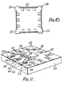
- Figure 10 shows a variation in which the base 5 and the spacer 8 (Fig 1) are arranged to provide lugs 29 at the corners of the finished circuit unit to facilitate correct location and alignment of the circuit unit and its contacts 6 and 12 when used in a rack arrangement or similar.
- the spacer 8 could be made of resilient insulating material which would thus help to provide increased contact pressure for the contacts 6 and 12 when the unit is inserted in a suitable slotted holder.
- the contacts 6 and 12 are arranged to stand slightly proud from the upper and lower surfaces of the circuit unit.
- Cooling may be improved by arranging for the material of the base 5 and/or the spacer 8 and/or the top layer 20 to be made of heat dissipating material.
- circuit unit described is not restricted to use as a chip carrier. Any suitable circuit device may be incorporated within the unit instead of an integrated circuit chip, and electrical connections made to the contacts in the manner shown.
- the circuit device incorporated could be a rechargeable or non-rechargeable cell or battery. Instead, however, there may be no actual circuit device within the unit.
- one of the racked units could be an interconnection unit as just described, and if the other units on either side of it were carrying chips, for example, the interconnection unit would provide a predetermined pattern of interconnections which, via the contacts 6 and 12 of all three units, would make the required interconnections between different parts of the chips in the adjacent chip carriers.
- Figure 11 shows another one of the circuit units which differs from the unit of Figure 1 in that it is made of a single layer, 30, of insulating material instead of the three layers 5, 8 and 20 of the unit of Figure 1.
- the single layer 30 of insulating material (which may be of the material described above for example) has contact pads 32 plated to its upper surface along its four sides and contacts 34 similarly plated to its under surface.
- a circuit element 36 which may again be an integrated circuit or chip (but could be any other suitable form of circuit device) is placed and bonded to the layer 30 in a suitable manner. If desired, the circuit device 36 could be placed within a suitably shaped recess.
- Connections 38 connect various parts of the circuit device 36 to the upper contacts 32, such as by a wire bonding process of normal form.
- Connections 40 similarly connect the circuit device 36 to the lower contacts 34.
- the connections 40 are made to intermediate contact pads 42 on the upper surface of the layer 30, these being in turn connected to respective ones of the contacts 34 via plated-through holes 44.
- Other means of making connections through the layer 30 to the contacts 34 could be used instead.
- the circuit device 36 may be encapsulated in any suitable way by applying an encapsulant over it.
- the single layer form showing in Figure 11 is particularly suited for use with tape-automated bonding systems.
- Figures 12 to 14 show a modified form of the circuit of Figure 11 and illustrate how a circuit device may then be placed in position thereon by means of a tape-automated-bonding system.
- Figure 12 illustrates the circuit unit which is similar to that shown in Figure 11 except that it does not have the contact pads 42 and the plated-through holes 44, and has its centre removed to provide an opening 50.
- the contacts 34 are of course not visible in Figure 8.
- Figure 13 shows a series of chips 36 mounted on leads 52 in openings 54 in a tape 56 in the normal tape-automated-bonding manner.
- the tape 56 is indexed over the chip carrier and when one of the chips 36 carried by the tape 56 is positioned over the opening 50 (Fig 12), the chip is removed from of the tape 56 and on to the chip carrier as shown in Figure 14, the leads 52 becoming bonded to appropriate ones of the contacts 32 to make the required electrical connections.
- Figure 15 shows the reverse side of the chip carrier with bonding pads 58 on the underside of the chip 36. By means of these pads, the chip is electrically connected to appropriate ones of the contacts 34 by wire connections 60.
- the chip is then encapsulated in a suitable encapsulant material.
- the insulating material 30 in multilayer form with conductive layers between the insulating layers to provide a capacitive effect, the conductive layers being suitably electrically connected to particular ones of the contacts 6, 12.
- the circuit units may be of any suitable size and can have any suitable number of contacts.
- a circuit unit of square configuration and having sides of 37 millimetres (one and half inches) could have ten or eleven contacts per edge at a pitch of 2.5 millimetres (0.1 inches) or twice that number of contacts at half the pitch.
- the circuit units are of square configuration, this is not essential. They could be of any other suitable configuration.
Landscapes
- Wire Bonding (AREA)
- Coupling Device And Connection With Printed Circuit (AREA)
- Structures For Mounting Electric Components On Printed Circuit Boards (AREA)
- Connecting Device With Holders (AREA)
Abstract
Claims (13)
Applications Claiming Priority (2)
| Application Number | Priority Date | Filing Date | Title |
|---|---|---|---|
| GB8222947 | 1982-08-10 | ||
| GB8222947 | 1982-08-10 |
Publications (2)
| Publication Number | Publication Date |
|---|---|
| EP0115514A1 EP0115514A1 (fr) | 1984-08-15 |
| EP0115514B1 true EP0115514B1 (fr) | 1986-11-12 |
Family
ID=10532209
Family Applications (1)
| Application Number | Title | Priority Date | Filing Date |
|---|---|---|---|
| EP83902536A Expired EP0115514B1 (fr) | 1982-08-10 | 1983-08-08 | Support de circuit integre |
Country Status (10)
| Country | Link |
|---|---|
| US (1) | US4638348A (fr) |
| EP (1) | EP0115514B1 (fr) |
| JP (1) | JPS59501564A (fr) |
| AT (1) | AT398254B (fr) |
| CA (1) | CA1211859A (fr) |
| CH (1) | CH659541A5 (fr) |
| DE (1) | DE3367699D1 (fr) |
| GB (1) | GB2127217B (fr) |
| IT (1) | IT1194368B (fr) |
| WO (1) | WO1984000851A1 (fr) |
Families Citing this family (63)
| Publication number | Priority date | Publication date | Assignee | Title |
|---|---|---|---|---|
| DE3603947A1 (de) * | 1986-02-06 | 1987-08-13 | Stiehl Hans Henrich Dr | System zur dosierung von luftgetragenen ionen mit hoher genauigkeit und verbessertem wirkungsgrad zur eliminierung elektrostatischer flaechenladungen |
| JPS63502866A (ja) * | 1986-03-25 | 1988-10-20 | ダウティ エレクトロニック コンポ−ネンツ リミティド | 電気回路の相互接続システム |
| US4991927A (en) * | 1986-03-25 | 1991-02-12 | Dowty Electronic Components Limited | Interconnection systems for electrical circuits |
| US4858072A (en) * | 1987-11-06 | 1989-08-15 | Ford Aerospace & Communications Corporation | Interconnection system for integrated circuit chips |
| US4956694A (en) * | 1988-11-04 | 1990-09-11 | Dense-Pac Microsystems, Inc. | Integrated circuit chip stacking |
| US4907128A (en) * | 1988-12-15 | 1990-03-06 | Grumman Aerospace Corporation | Chip to multilevel circuit board bonding |
| US4912547A (en) * | 1989-01-30 | 1990-03-27 | International Business Machines Corporation | Tape bonded semiconductor device |
| US5502278A (en) * | 1989-05-30 | 1996-03-26 | Thomson Composants Militaires Et Spatiaux | Encased electronic circuit with chip on a grid zone of conductive contacts |
| US5089878A (en) * | 1989-06-09 | 1992-02-18 | Lee Jaesup N | Low impedance packaging |
| GB2236020A (en) * | 1989-09-12 | 1991-03-20 | Plessey Co Plc | Electronic circuit package |
| US5008492A (en) * | 1989-10-20 | 1991-04-16 | Hughes Aircraft Company | High current feedthrough package |
| USD323318S (en) | 1989-12-18 | 1992-01-21 | International Business Machines Corporation | Magazine for a plurality of tube assemblies carrying integrated circuit chips |
| US5191404A (en) * | 1989-12-20 | 1993-03-02 | Digital Equipment Corporation | High density memory array packaging |
| US5148265A (en) | 1990-09-24 | 1992-09-15 | Ist Associates, Inc. | Semiconductor chip assemblies with fan-in leads |
| US5043794A (en) * | 1990-09-24 | 1991-08-27 | At&T Bell Laboratories | Integrated circuit package and compact assemblies thereof |
| JPH0715969B2 (ja) * | 1991-09-30 | 1995-02-22 | インターナショナル・ビジネス・マシーンズ・コーポレイション | マルチチツプ集積回路パツケージ及びそのシステム |
| DE69330450T2 (de) * | 1992-08-05 | 2001-11-08 | Fujitsu Ltd., Kawasaki | Dreidimensionaler Multichipmodul |
| US5854534A (en) * | 1992-08-05 | 1998-12-29 | Fujitsu Limited | Controlled impedence interposer substrate |
| US5754399A (en) * | 1992-09-30 | 1998-05-19 | International Business Machines Corporation | Direct coupled CPU package |
| US6205654B1 (en) * | 1992-12-11 | 2001-03-27 | Staktek Group L.P. | Method of manufacturing a surface mount package |
| US5528463A (en) * | 1993-07-16 | 1996-06-18 | Dallas Semiconductor Corp. | Low profile sockets and modules for surface mountable applications |
| US5561622A (en) * | 1993-09-13 | 1996-10-01 | International Business Machines Corporation | Integrated memory cube structure |
| US5502667A (en) * | 1993-09-13 | 1996-03-26 | International Business Machines Corporation | Integrated multichip memory module structure |
| US5929517A (en) | 1994-12-29 | 1999-07-27 | Tessera, Inc. | Compliant integrated circuit package and method of fabricating the same |
| US5514907A (en) * | 1995-03-21 | 1996-05-07 | Simple Technology Incorporated | Apparatus for stacking semiconductor chips |
| US5648684A (en) * | 1995-07-26 | 1997-07-15 | International Business Machines Corporation | Endcap chip with conductive, monolithic L-connect for multichip stack |
| US6861290B1 (en) * | 1995-12-19 | 2005-03-01 | Micron Technology, Inc. | Flip-chip adaptor package for bare die |
| US5825084A (en) * | 1996-08-22 | 1998-10-20 | Express Packaging Systems, Inc. | Single-core two-side substrate with u-strip and co-planar signal traces, and power and ground planes through split-wrap-around (SWA) or split-via-connections (SVC) for packaging IC devices |
| RU2133523C1 (ru) * | 1997-11-03 | 1999-07-20 | Закрытое акционерное общество "Техно-ТМ" | Трехмерный электронный модуль |
| KR19990058460A (ko) * | 1997-12-30 | 1999-07-15 | 김영환 | 스택 칩 패키지 |
| US6121679A (en) * | 1998-03-10 | 2000-09-19 | Luvara; John J. | Structure for printed circuit design |
| US6310303B1 (en) | 1998-03-10 | 2001-10-30 | John J. Luvara | Structure for printed circuit design |
| US6552264B2 (en) | 1998-03-11 | 2003-04-22 | International Business Machines Corporation | High performance chip packaging and method |
| US6072233A (en) | 1998-05-04 | 2000-06-06 | Micron Technology, Inc. | Stackable ball grid array package |
| USRE43112E1 (en) | 1998-05-04 | 2012-01-17 | Round Rock Research, Llc | Stackable ball grid array package |
| US6121576A (en) * | 1998-09-02 | 2000-09-19 | Micron Technology, Inc. | Method and process of contact to a heat softened solder ball array |
| RU2134466C1 (ru) * | 1998-12-08 | 1999-08-10 | Таран Александр Иванович | Носитель кристалла ис |
| US6572387B2 (en) | 1999-09-24 | 2003-06-03 | Staktek Group, L.P. | Flexible circuit connector for stacked chip module |
| US6608763B1 (en) | 2000-09-15 | 2003-08-19 | Staktek Group L.P. | Stacking system and method |
| US6462408B1 (en) * | 2001-03-27 | 2002-10-08 | Staktek Group, L.P. | Contact member stacking system and method |
| US20030002267A1 (en) * | 2001-06-15 | 2003-01-02 | Mantz Frank E. | I/O interface structure |
| US6573461B2 (en) | 2001-09-20 | 2003-06-03 | Dpac Technologies Corp | Retaining ring interconnect used for 3-D stacking |
| US6573460B2 (en) | 2001-09-20 | 2003-06-03 | Dpac Technologies Corp | Post in ring interconnect using for 3-D stacking |
| US6977440B2 (en) * | 2001-10-09 | 2005-12-20 | Tessera, Inc. | Stacked packages |
| US7335995B2 (en) * | 2001-10-09 | 2008-02-26 | Tessera, Inc. | Microelectronic assembly having array including passive elements and interconnects |
| US6897565B2 (en) * | 2001-10-09 | 2005-05-24 | Tessera, Inc. | Stacked packages |
| US7081373B2 (en) | 2001-12-14 | 2006-07-25 | Staktek Group, L.P. | CSP chip stack with flex circuit |
| US6765288B2 (en) * | 2002-08-05 | 2004-07-20 | Tessera, Inc. | Microelectronic adaptors, assemblies and methods |
| WO2004017399A1 (fr) * | 2002-08-16 | 2004-02-26 | Tessera, Inc. | Boitiers microelectroniques a alignement automatique |
| US7294928B2 (en) * | 2002-09-06 | 2007-11-13 | Tessera, Inc. | Components, methods and assemblies for stacked packages |
| US7071547B2 (en) * | 2002-09-11 | 2006-07-04 | Tessera, Inc. | Assemblies having stacked semiconductor chips and methods of making same |
| EP1546988B1 (fr) * | 2002-09-25 | 2007-02-14 | Koninklijke Philips Electronics N.V. | Connecteur pour carte a puce |
| US6856010B2 (en) * | 2002-12-05 | 2005-02-15 | Staktek Group L.P. | Thin scale outline package |
| US6840794B2 (en) * | 2003-03-31 | 2005-01-11 | Intel Corporation | Apparatus and methods for cooling a processor socket |
| US20040207990A1 (en) * | 2003-04-21 | 2004-10-21 | Rose Andrew C. | Stair-step signal routing |
| US7061121B2 (en) | 2003-11-12 | 2006-06-13 | Tessera, Inc. | Stacked microelectronic assemblies with central contacts |
| US7545029B2 (en) * | 2006-08-18 | 2009-06-09 | Tessera, Inc. | Stack microelectronic assemblies |
| US7763983B2 (en) * | 2007-07-02 | 2010-07-27 | Tessera, Inc. | Stackable microelectronic device carriers, stacked device carriers and methods of making the same |
| US9429983B1 (en) | 2013-09-12 | 2016-08-30 | Advanced Processor Architectures, Llc | System clock distribution in a distributed computing environment |
| US8381031B2 (en) | 2009-08-07 | 2013-02-19 | Advanced Processor Architectures, Llc | Distributed computing |
| US9645603B1 (en) | 2013-09-12 | 2017-05-09 | Advanced Processor Architectures, Llc | System clock distribution in a distributed computing environment |
| US11042211B2 (en) | 2009-08-07 | 2021-06-22 | Advanced Processor Architectures, Llc | Serially connected computing nodes in a distributed computing system |
| CN113838812B (zh) * | 2020-06-23 | 2025-06-10 | 桑迪士克科技股份有限公司 | 高速存储卡的侧面接触垫 |
Family Cites Families (16)
| Publication number | Priority date | Publication date | Assignee | Title |
|---|---|---|---|---|
| US3404215A (en) * | 1966-04-14 | 1968-10-01 | Sprague Electric Co | Hermetically sealed electronic module |
| US3614541A (en) * | 1969-04-08 | 1971-10-19 | North American Rockwell | Package for an electronic assembly |
| JPS4919023B1 (fr) * | 1970-01-02 | 1974-05-14 | ||
| DE2124887C3 (de) * | 1971-05-19 | 1980-04-17 | Philips Patentverwaltung Gmbh, 2000 Hamburg | Elektrisches Bauelement, vorzugsweise Halbleiterbauelement, mit Folienkontaktierung |
| JPS5619040B2 (fr) * | 1974-05-16 | 1981-05-02 | ||
| JPS5810857B2 (ja) * | 1975-05-28 | 1983-02-28 | 株式会社東芝 | デンシカイロソウチ |
| JPS5914894B2 (ja) * | 1978-08-03 | 1984-04-06 | 日本碍子株式会社 | セラミツクパツケ−ジ |
| JPS55115351A (en) * | 1979-02-26 | 1980-09-05 | Fujitsu Ltd | Ic stem |
| JPS55124248A (en) * | 1979-03-20 | 1980-09-25 | Nec Corp | Leadless package |
| DE3030763A1 (de) * | 1979-08-17 | 1981-03-26 | Amdahl Corp., Sunnyvale, Calif. | Packung fuer eine integrierte schaltung in plaettchenform |
| JPS56126948A (en) * | 1980-03-12 | 1981-10-05 | Hitachi Ltd | Highly integrated semiconductor |
| US4320438A (en) * | 1980-05-15 | 1982-03-16 | Cts Corporation | Multi-layer ceramic package |
| GB2056772B (en) * | 1980-08-12 | 1983-09-01 | Amdahl Corp | Integrated circuit package and module |
| JPS57115850A (en) * | 1981-01-10 | 1982-07-19 | Nec Corp | Chip carrier for semiconductor ic |
| GB2095039B (en) * | 1981-02-10 | 1984-09-19 | Brown David F | Circuit assembly |
| FR2501414A1 (fr) * | 1981-03-06 | 1982-09-10 | Thomson Csf | Microboitier d'encapsulation de pastilles de semi-conducteur, testable apres soudure sur un substrat |
-
1983
- 1983-08-08 US US06/595,454 patent/US4638348A/en not_active Expired - Fee Related
- 1983-08-08 AT AT0904383A patent/AT398254B/de not_active IP Right Cessation
- 1983-08-08 DE DE8383902536T patent/DE3367699D1/de not_active Expired
- 1983-08-08 EP EP83902536A patent/EP0115514B1/fr not_active Expired
- 1983-08-08 WO PCT/GB1983/000198 patent/WO1984000851A1/fr not_active Ceased
- 1983-08-08 JP JP58502589A patent/JPS59501564A/ja active Pending
- 1983-08-08 CH CH1763/84A patent/CH659541A5/fr not_active IP Right Cessation
- 1983-08-09 GB GB08321375A patent/GB2127217B/en not_active Expired
- 1983-08-09 IT IT8322493A patent/IT1194368B/it active
- 1983-08-09 CA CA000434207A patent/CA1211859A/fr not_active Expired
Also Published As
| Publication number | Publication date |
|---|---|
| DE3367699D1 (en) | 1987-01-02 |
| GB8321375D0 (en) | 1983-09-07 |
| GB2127217A (en) | 1984-04-04 |
| CH659541A5 (fr) | 1987-01-30 |
| GB2127217B (en) | 1986-05-08 |
| CA1211859A (fr) | 1986-09-23 |
| ATA904383A (de) | 1994-02-15 |
| IT1194368B (it) | 1988-09-22 |
| IT8322493A0 (it) | 1983-08-09 |
| AT398254B (de) | 1994-11-25 |
| WO1984000851A1 (fr) | 1984-03-01 |
| US4638348A (en) | 1987-01-20 |
| JPS59501564A (ja) | 1984-08-30 |
| EP0115514A1 (fr) | 1984-08-15 |
Similar Documents
| Publication | Publication Date | Title |
|---|---|---|
| US4638348A (en) | Semiconductor chip carrier | |
| EP0067677B1 (fr) | Dispositif semiconducteur ayant la structure d'une série de puces | |
| EP0546731B1 (fr) | Structure de conducteurs internes d'un dispositif semi-conducteur | |
| KR101062260B1 (ko) | 집적 회로 조립체 | |
| US4147889A (en) | Chip carrier | |
| US5397916A (en) | Semiconductor device including stacked die | |
| CA1201820A (fr) | Circuit integre a semiconducteur comprenant un cadre de montage de puce avec supports | |
| US5648679A (en) | Tape ball lead integrated circuit package | |
| US5281852A (en) | Semiconductor device including stacked die | |
| US4459607A (en) | Tape automated wire bonded integrated circuit chip assembly | |
| US4496965A (en) | Stacked interdigitated lead frame assembly | |
| US4796078A (en) | Peripheral/area wire bonding technique | |
| US5229960A (en) | Solid state memory modules and memory devices including such modules | |
| US4812949A (en) | Method of and apparatus for mounting an IC chip | |
| US5840599A (en) | Process of packaging an integrated circuit with a conductive material between a lead frame and the face of the circuit | |
| US5847935A (en) | Electronic circuit chip package | |
| JPH0744239B2 (ja) | チツプ・キヤリアと集積半導体チツプを有するモジユール | |
| JP2003533787A (ja) | チップカード | |
| KR20010078712A (ko) | 칩 스택 및 그 제조 방법 | |
| CA1297998C (fr) | Systeme d'interconnexion pour puces de circuits integres | |
| JPH0357257A (ja) | 高密度半導体メモリモジユール及びその形成方法 | |
| ATE54776T1 (de) | Halbleiterelement und herstellungsverfahren. | |
| EP0405871A2 (fr) | Cadre de connexion à capacité équilibrée pour circuits intégrés | |
| US4380357A (en) | System and method for effecting electrical interconnections using a flexible media with radially extending electrical conductors | |
| JPH023621Y2 (fr) |
Legal Events
| Date | Code | Title | Description |
|---|---|---|---|
| PUAI | Public reference made under article 153(3) epc to a published international application that has entered the european phase |
Free format text: ORIGINAL CODE: 0009012 |
|
| AK | Designated contracting states |
Kind code of ref document: A1 Designated state(s): BE DE FR NL SE |
|
| 17P | Request for examination filed |
Effective date: 19840808 |
|
| GRAA | (expected) grant |
Free format text: ORIGINAL CODE: 0009210 |
|
| AK | Designated contracting states |
Kind code of ref document: B1 Designated state(s): BE DE FR NL SE |
|
| ET | Fr: translation filed | ||
| BECA | Be: change of holder's address |
Free format text: 861112 *DOWTY ELECTRONIC COMPONENTS LTDFASSETTS ROAD, LOUDWATER BUCKINGHAMSHIRE |
|
| BECH | Be: change of holder |
Free format text: 861112 *DOWTY ELECTRONIC COMPONENTS LTD |
|
| REF | Corresponds to: |
Ref document number: 3367699 Country of ref document: DE Date of ref document: 19870102 |
|
| PLBE | No opposition filed within time limit |
Free format text: ORIGINAL CODE: 0009261 |
|
| STAA | Information on the status of an ep patent application or granted ep patent |
Free format text: STATUS: NO OPPOSITION FILED WITHIN TIME LIMIT |
|
| 26N | No opposition filed | ||
| REG | Reference to a national code |
Ref country code: FR Ref legal event code: TP |
|
| BECA | Be: change of holder's address |
Free format text: 880226 *DOWTY ELECTRONIC COMPONENTS LTD:FASSETTS ROAD, LOUDWATER BUCKINGHAMSHIRE |
|
| BECH | Be: change of holder |
Free format text: 880226 *DOWTY ELECTRONIC COMPONENTS LTD |
|
| EAL | Se: european patent in force in sweden |
Ref document number: 83902536.8 |
|
| PGFP | Annual fee paid to national office [announced via postgrant information from national office to epo] |
Ref country code: FR Payment date: 19970811 Year of fee payment: 15 |
|
| PGFP | Annual fee paid to national office [announced via postgrant information from national office to epo] |
Ref country code: SE Payment date: 19970818 Year of fee payment: 15 Ref country code: DE Payment date: 19970818 Year of fee payment: 15 |
|
| PGFP | Annual fee paid to national office [announced via postgrant information from national office to epo] |
Ref country code: NL Payment date: 19970826 Year of fee payment: 15 |
|
| PGFP | Annual fee paid to national office [announced via postgrant information from national office to epo] |
Ref country code: BE Payment date: 19970925 Year of fee payment: 15 |
|
| PG25 | Lapsed in a contracting state [announced via postgrant information from national office to epo] |
Ref country code: SE Free format text: LAPSE BECAUSE OF NON-PAYMENT OF DUE FEES Effective date: 19980809 |
|
| PG25 | Lapsed in a contracting state [announced via postgrant information from national office to epo] |
Ref country code: BE Free format text: LAPSE BECAUSE OF NON-PAYMENT OF DUE FEES Effective date: 19980831 |
|
| BERE | Be: lapsed |
Owner name: DOWTY ELECTRONIC COMPONENTS LTD Effective date: 19980831 |
|
| PG25 | Lapsed in a contracting state [announced via postgrant information from national office to epo] |
Ref country code: NL Free format text: LAPSE BECAUSE OF NON-PAYMENT OF DUE FEES Effective date: 19990301 |
|
| PG25 | Lapsed in a contracting state [announced via postgrant information from national office to epo] |
Ref country code: FR Free format text: LAPSE BECAUSE OF NON-PAYMENT OF DUE FEES Effective date: 19990430 |
|
| EUG | Se: european patent has lapsed |
Ref document number: 83902536.8 |
|
| NLV4 | Nl: lapsed or anulled due to non-payment of the annual fee |
Effective date: 19990301 |
|
| PG25 | Lapsed in a contracting state [announced via postgrant information from national office to epo] |
Ref country code: DE Free format text: LAPSE BECAUSE OF NON-PAYMENT OF DUE FEES Effective date: 19990601 |
|
| REG | Reference to a national code |
Ref country code: FR Ref legal event code: ST |