EP0120500A2 - LSI Verpackung hoher Dichte für logische Schaltungen - Google Patents
LSI Verpackung hoher Dichte für logische Schaltungen Download PDFInfo
- Publication number
- EP0120500A2 EP0120500A2 EP84103423A EP84103423A EP0120500A2 EP 0120500 A2 EP0120500 A2 EP 0120500A2 EP 84103423 A EP84103423 A EP 84103423A EP 84103423 A EP84103423 A EP 84103423A EP 0120500 A2 EP0120500 A2 EP 0120500A2
- Authority
- EP
- European Patent Office
- Prior art keywords
- substrate
- chip
- wiring layers
- chip carrier
- chips
- Prior art date
- Legal status (The legal status is an assumption and is not a legal conclusion. Google has not performed a legal analysis and makes no representation as to the accuracy of the status listed.)
- Granted
Links
Images




Classifications
-
- H—ELECTRICITY
- H10—SEMICONDUCTOR DEVICES; ELECTRIC SOLID-STATE DEVICES NOT OTHERWISE PROVIDED FOR
- H10W—GENERIC PACKAGES, INTERCONNECTIONS, CONNECTORS OR OTHER CONSTRUCTIONAL DETAILS OF DEVICES COVERED BY CLASS H10
- H10W70/00—Package substrates; Interposers; Redistribution layers [RDL]
- H10W70/60—Insulating or insulated package substrates; Interposers; Redistribution layers
- H10W70/611—Insulating or insulated package substrates; Interposers; Redistribution layers for connecting multiple chips together
-
- H—ELECTRICITY
- H10—SEMICONDUCTOR DEVICES; ELECTRIC SOLID-STATE DEVICES NOT OTHERWISE PROVIDED FOR
- H10W—GENERIC PACKAGES, INTERCONNECTIONS, CONNECTORS OR OTHER CONSTRUCTIONAL DETAILS OF DEVICES COVERED BY CLASS H10
- H10W70/00—Package substrates; Interposers; Redistribution layers [RDL]
- H10W70/60—Insulating or insulated package substrates; Interposers; Redistribution layers
- H10W70/62—Insulating or insulated package substrates; Interposers; Redistribution layers characterised by their interconnections
- H10W70/63—Vias, e.g. via plugs
- H10W70/635—Through-vias
-
- H—ELECTRICITY
- H10—SEMICONDUCTOR DEVICES; ELECTRIC SOLID-STATE DEVICES NOT OTHERWISE PROVIDED FOR
- H10W—GENERIC PACKAGES, INTERCONNECTIONS, CONNECTORS OR OTHER CONSTRUCTIONAL DETAILS OF DEVICES COVERED BY CLASS H10
- H10W70/00—Package substrates; Interposers; Redistribution layers [RDL]
- H10W70/60—Insulating or insulated package substrates; Interposers; Redistribution layers
- H10W70/67—Insulating or insulated package substrates; Interposers; Redistribution layers characterised by their insulating layers or insulating parts
- H10W70/68—Shapes or dispositions thereof
- H10W70/685—Shapes or dispositions thereof comprising multiple insulating layers
-
- H—ELECTRICITY
- H10—SEMICONDUCTOR DEVICES; ELECTRIC SOLID-STATE DEVICES NOT OTHERWISE PROVIDED FOR
- H10W—GENERIC PACKAGES, INTERCONNECTIONS, CONNECTORS OR OTHER CONSTRUCTIONAL DETAILS OF DEVICES COVERED BY CLASS H10
- H10W76/00—Containers; Fillings or auxiliary members therefor; Seals
- H10W76/10—Containers or parts thereof
- H10W76/12—Containers or parts thereof characterised by their shape
- H10W76/15—Containers comprising an insulating or insulated base
- H10W76/153—Containers comprising an insulating or insulated base having interconnections in passages through the insulating or insulated base
-
- H—ELECTRICITY
- H10—SEMICONDUCTOR DEVICES; ELECTRIC SOLID-STATE DEVICES NOT OTHERWISE PROVIDED FOR
- H10W—GENERIC PACKAGES, INTERCONNECTIONS, CONNECTORS OR OTHER CONSTRUCTIONAL DETAILS OF DEVICES COVERED BY CLASS H10
- H10W90/00—Package configurations
-
- H—ELECTRICITY
- H10—SEMICONDUCTOR DEVICES; ELECTRIC SOLID-STATE DEVICES NOT OTHERWISE PROVIDED FOR
- H10W—GENERIC PACKAGES, INTERCONNECTIONS, CONNECTORS OR OTHER CONSTRUCTIONAL DETAILS OF DEVICES COVERED BY CLASS H10
- H10W72/00—Interconnections or connectors in packages
- H10W72/071—Connecting or disconnecting
- H10W72/072—Connecting or disconnecting of bump connectors
- H10W72/07251—Connecting or disconnecting of bump connectors characterised by changes in properties of the bump connectors during connecting
-
- H—ELECTRICITY
- H10—SEMICONDUCTOR DEVICES; ELECTRIC SOLID-STATE DEVICES NOT OTHERWISE PROVIDED FOR
- H10W—GENERIC PACKAGES, INTERCONNECTIONS, CONNECTORS OR OTHER CONSTRUCTIONAL DETAILS OF DEVICES COVERED BY CLASS H10
- H10W72/00—Interconnections or connectors in packages
- H10W72/20—Bump connectors, e.g. solder bumps or copper pillars; Dummy bumps; Thermal bumps
-
- H—ELECTRICITY
- H10—SEMICONDUCTOR DEVICES; ELECTRIC SOLID-STATE DEVICES NOT OTHERWISE PROVIDED FOR
- H10W—GENERIC PACKAGES, INTERCONNECTIONS, CONNECTORS OR OTHER CONSTRUCTIONAL DETAILS OF DEVICES COVERED BY CLASS H10
- H10W72/00—Interconnections or connectors in packages
- H10W72/851—Dispositions of multiple connectors or interconnections
- H10W72/874—On different surfaces
- H10W72/877—Bump connectors and die-attach connectors
-
- H—ELECTRICITY
- H10—SEMICONDUCTOR DEVICES; ELECTRIC SOLID-STATE DEVICES NOT OTHERWISE PROVIDED FOR
- H10W—GENERIC PACKAGES, INTERCONNECTIONS, CONNECTORS OR OTHER CONSTRUCTIONAL DETAILS OF DEVICES COVERED BY CLASS H10
- H10W90/00—Package configurations
- H10W90/20—Configurations of stacked chips
Definitions
- This invention relates to a high density large scale integrated (LSI) package for logic circuits for use in data processing and communications systems.
- LSI large scale integrated
- LSI packages for logic circuits are indispensable to realize faster and more compact systems.
- packages having active elements such as transistors require a structure to diffuse the heat generated by electric power consumption.
- a multi-chip package having such a heat diffusing structure is proposed in a paper by Hajime Nakamura et al. entitled “Manufacturing Technology of High Circuit Density Multi-Layer Substrates", IEEE, TRANSACTIONS ON COMPUTERS, HYBRIDS, AND MANUFACTURING TECHNOLOGY, VOL. CHMT-4, No. 2., June 1981 issue, pp. 333-337.
- the substrate of the package illustrated in Fig. 10 of this paper on page 337 is composed of an alumina ceramic. Multiple signal wiring layers.and a power bus layer are formed on the surface of the substrate. An IC ship mounted over the substrate is connected to these wiring layers. To the undersurface of the substrate is stuck a heat sink for diffusing the heat from the IC chip.
- the multi-layer wiring substrate of this structure has the following disadvantages.
- One primary object of the present invention is to provide a high density multi-chip package ensuring a high signal propagation speed by the application of fine wiring, which is free from the above-mentioned disadvantages.
- Another object of the invention is to provide a multi-chip package with a high heat diffusing efficiency by mounting leadless chip carriers in a face-down position.
- a multi-chip package which comprises;
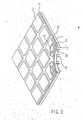
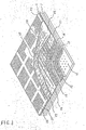
- one embodiment of the invention comprises an alumina ceramic substrate 1, multiple wiring layers 2 of organic high polymer, formed over the upper surface of this substrate 1, and a plurality of leadless chip carriers 3.
- a plurality of input and output terminal pins 11 are formed on the under-surface of the alumina ceramic substrate 1 in a grid shape.
- the sticking of the input and output terminal pins 11 to the alumina ceramic substrate 1 is achieved by nickel-plating metallic bases, primarily made of tungsten, on the alumina ceramic substrates 1, applying solder, such as silver-copper eutectic brazing solder, over the plating, and, with the metallic terminal pins 11 pressed against the bases, melting and then hardening the solder.
- solder such as silver-copper eutectic brazing solder
- the input and output pins 11 are arranged in a grid form all over the under surface of the substrate 1, there can be provided far more pins than where such pins are arranged only on the peripheries of the substrate 1.
- through-hole wires 12 penetrate the substrate 1 from the under surface to the upper surface of the substrate 1. These wires 12 electrically connect the input and output terminals 11 to wiring formed over the upper surface of said substrate 1.
- a power supply wiring layer 13 and a ground wiring layer 14 are connected to what are respectively designated for power supply and grounding among the . input and output pins 11. These wiring layers 13 and 14 provide power and ground potentials for IC chips connected to the upper surface of the substrate 1.
- those of the input and output pins 11 which are used as signal pins are connected by way of the through-hole wires 12 and the wiring on the upper surface of the substrate 1 to wiring within the multiple wiring layers 2.
- those of the input and output pins 11 which are used for power supply and grounding are respectively connected to the power supply wiring layer 13 and the ground wiring layer 14 within the substrate 1.
- the signal wiring within the multiple wiring layers 2 connects chip carrier terminals 34 of the leadless chip carriers 3 in some combinations. This signal wiring also connects some signal terminals of the leadless chip carriers 3 to some of the input and output pins 11.
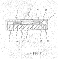
- Each leadless chip carrier 3 is provided with a chip carrier substrate 31, an IC chip 32 and a chip carrier cover 33.
- the IC chip 32 is lead-bonded face down to the substrate 31, and is die-bonded to the cover 33.
- the chip carrier cover 33 is made of either a highly heat-conductive metal, such as ferro-nickel alloy or cobalt-nickel alloy, or a highly heat-conductive insulator, such as beryllia. Therefore, the heat generated by the IC chip 32 can be very efficiently transmitted to the surface of the cover 33.
- a heat diffusing cover 41 in either direct or almost direct contact with the chip carriers 3 is fitted to the alumina ceramic substrate 1. Further a liquid cooling board 42 is in contact with this cover 41.
- the board 42 is provided with a channel 43 for letting coolant flow, an inlet 44 for supplying the coolant into this channel 43 and an outlet 45 for the coolant.
- a heat-conductive filter 46 fills the gap between the cover 41 and the substrate 1.
- the cooling performance can be further improved.
- the multi-chip package according to the present invention can provide the following effects:
- FIGS. 1 through 4 the embodiment of the present invention will be described in further detail.
- the IC chip 32 is lead-bonded face down onto the chip carrier substrate 31 and die-bonded to the chip carrier cover 33. Further, the chip carriers 3 are connected to inner wiring within the multiple wiring layers 2 by way of chip carrier terminals 34. The input and output pins 11 on the under-face of the substrate 1 are connected to the inner wiring within the multiple wiring layers 2 through the through-hole wires 12.
- the substrate 1 contains a power supply wiring layer 13, a ground wiring layer 14 and the through-hole wires 12 connecting the input and output pins 11 and the multiple wiring layers 2.
- a power supply wiring layer 13 a ground wiring layer 14 and the through-hole wires 12 connecting the input and output pins 11 and the multiple wiring layers 2.
- the multiple wiring layers 2 comprises a first wiring layer further having thin-film conductive wiring 24 formed over an insulating film 21 made of organic high polymer and a plurality of via-holes 27 for connection to the through-hole wires of the layer underneath, a second wiring layer having thin-film conductive wiring 25 similarly formed over an insulating film 22 and a plurality of via-holes 28 for connection of the wiring 24 and wiring 25, and a third wiring layer having an insulating film 23, a plurality of terminal pads 26 for connecting the terminals 34 of the carriers 3 on the surface of the film 23, and a plurality of via-holes 29 for connecting the pads 26 and the wiring 25. Therefore, the multiple wiring layers 2 can connect the terminals 34 of any desired ones of the carriers 3 to one another, and any. desired ones of the terminals 34 to any desired ones of the input and output pins 11.
- the leadless chip carrier illustrated in FIG. 4 is assembled by the following procedure: first, an IC chip 32 to which leads 37 are bonded onto the chip carrier substrate 31 is placed in a face-down position; next, after the relative positions of the leads 37 and an outer lead bonding pads 38 on the substrate 31 are adjusted, all the leads are bonded collectively; in this state, all the bumps 311 are conductively connected to all the chip carrier terminals 34 by way of the pads 38, connecting wires 39 and chip carrier through-hole wires 310.
- TAB tape automatic bonding
- the chip carrier cover 33 to which a die bonding adhesive 35 and a substrate adhesive 36 have been applied, is placed the chip carrier substrate 31, to which the IC the chip 32 is bounded face down so that/cover 33 comes into contact wi the die of the IC chip 32. After that, heat needed for hardening the adhesives 35 and 36 is impressed to complete the bonding. In this manner, the high-density, high- performance multi-chip package can be produced by using the leadless chip carriers which are compact and highly efficient in heat diffusion.
- a plurality of IC chips 32 is connected to a chip carrier substrate 31.
- This chip carrier comprises the substrate 31, the IC chips 32, a chip carrier cover 33, chip carrier terminals 34, leads 37, bonding pads 38, terminal bumps 311, a substrate adhesive 36, a die bonding adhesive 35, chip carrier through-hole wires 310 and connecting wires 39.
- a plurality of bonding pads 38 are formed on the surface of the substrate 31.
- a lead 37 of one of the IC chips 32 is bonded to each of these pads 38.
- a plurality of connecting wires 39 are formed on the surface of the substrate 31.
- the wires 39 are connected to each of the pads 38.
- Each of these wires 39 is also connected to one of the chip carrier terminals 34 via one of the through-hole wires 310.
- a plurality of IC chips 32 and the chip carrier terminals 34 are directly connected to each other.
- the connection of one IC chip and another IC chip can also be achieved by way of a wiring layer within the substrate 31.
- each of the bonding pads 38 is connected to one of the wires 310 via a connecting wire 39. Further, each of these wires 310 penetrates the substrate 31 and is connected to one of the chip carrier terminals 34.
- the terminal 34 can be used for external connection.
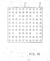
- the chip carrier terminals 34 are arranged in a grid form on the under-surface of the substrate 31. Accordingly, it is possible to take out many terminals in a high density. By utilizing this high terminal density to mount a plurality of multi-terminal IC chips on each chip carrier, there can be achieved high-density mounting in a very compact form.
- the leads 37 of the IC chip 32 are connected to corresponding ones of the terminal bumps 311 of the IC chip 32.
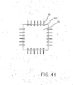
- the leads 37 can be produced by exposing to light, developing and etching copper foil over a film having sprocket holes by photolithography. After the leads 37 formed over the film are gold-plated, the leads 37 are bonded collectively to the terminal bumps 311 on the IC chip 32 by the known TAB technique. After that, each part of the film having supported the leads 37 is cut off to give an IC chip with TAB leads as shown in FIG. 11.
- the die bonding adhesive 35 for sticking the body of each IC chip 32.
- this adhesive there may be used a highly heat-conductive resin adhesive which can be hardened by impressing with heat of a predetermined temperature for a fixed length of time.
- a silver filter electrically conductive epoxy adhesive which is hardened by impressing with heat of 150°C for 30 minutes.
- each of the leads 37 of the IC chip 32 is bonded to one of the pads 38 of the substrate 31. Further the body of the IC chip 32 is fastened to the inside of the cover 33.
- Such a chip carrier is assembled in the following sequence: first, the IC chips 32, to which all its leads 37 have been connected in advance, are placed face down on the ceramic substrate 31, and each of the leads 37 is aligned to the corresponding.
- the leads 37 and the respectively corresponding bonding pads 38 are collectively bonded to each other; then the cover 33 is placed over the surface of the substrate 31, on which the IC chips 32 are mounted, and the adhesive 35 and the body of each IC chip 32 are brought into contact; in this condition, the adhesive 35 is hardened by impressing with heat of 150°C for a predetermined length of time, for instance 30 minutes, to bond together the cover 33 and each IC chip 32; next the epoxy adhesive 36 is injected between the mutually contacting faces of the substrate 31 and the cover 33, and is heated at 150°C for 90 minutes to bond them together; thus is completed the assembly of the chip carrier.
- the chip carrier can realize the advantages of having many input and output terminals, excelling in heat diffusing performance and being very small in size.
- the multi-chip package according to the present invention comprising a ceramic substrate with input' and output pins all over its under surface and high-speed multi-layer wiring made of organic high polymer on its upper surface, a leadless chip carrier excelling in heat diffusing performance to which IC chips can be directly die-bonded, and a cooling function arranged in the upper part of said chip carrier, has the benefit of making it possible to realize a high-speed, high-density and highly heat-diffusing multi-terminal multi-chip package and chip carrier.
Landscapes
- Wire Bonding (AREA)
- Cooling Or The Like Of Semiconductors Or Solid State Devices (AREA)
Applications Claiming Priority (6)
| Application Number | Priority Date | Filing Date | Title |
|---|---|---|---|
| JP52944/83 | 1983-03-29 | ||
| JP58052944A JPS59178759A (ja) | 1983-03-29 | 1983-03-29 | マルチチツプパツケ−ジ |
| JP73293/83 | 1983-04-26 | ||
| JP58073294A JPS59198738A (ja) | 1983-04-26 | 1983-04-26 | リ−ドレスマルチチツプチツプキヤリア |
| JP73294/83 | 1983-04-26 | ||
| JP58073293A JPS59198737A (ja) | 1983-04-26 | 1983-04-26 | リ−ドレスマルチチツプチツプキヤリア |
Publications (3)
| Publication Number | Publication Date |
|---|---|
| EP0120500A2 true EP0120500A2 (de) | 1984-10-03 |
| EP0120500A3 EP0120500A3 (en) | 1986-12-03 |
| EP0120500B1 EP0120500B1 (de) | 1989-08-16 |
Family
ID=27294796
Family Applications (1)
| Application Number | Title | Priority Date | Filing Date |
|---|---|---|---|
| EP84103423A Expired EP0120500B1 (de) | 1983-03-29 | 1984-03-28 | LSI Verpackung hoher Dichte für logische Schaltungen |
Country Status (4)
| Country | Link |
|---|---|
| US (2) | US4652970A (de) |
| EP (1) | EP0120500B1 (de) |
| CA (1) | CA1229155A (de) |
| DE (1) | DE3479463D1 (de) |
Cited By (9)
| Publication number | Priority date | Publication date | Assignee | Title |
|---|---|---|---|---|
| GB2181899A (en) * | 1985-08-21 | 1987-04-29 | Bass Plc | Electronic switches |
| WO1987006062A1 (en) * | 1986-03-27 | 1987-10-08 | Hughes Aircraft Company | Inverted chip carrier |
| EP0260969A1 (de) * | 1986-09-19 | 1988-03-23 | Nec Corporation | Chipträger |
| EP0260857A3 (en) * | 1986-09-08 | 1988-09-07 | Nec Corporation | Multilayer wiring substrate |
| EP0351581A1 (de) * | 1988-07-22 | 1990-01-24 | Oerlikon-Contraves AG | Hochintegrierte Schaltung sowie Verfahren zu deren Herstellung |
| EP0351184A3 (de) * | 1988-07-15 | 1990-08-16 | Advanced Micro Devices, Inc. | Packungsstruktur mit einem Steckerstift-Gitter |
| EP0361495A3 (de) * | 1988-09-30 | 1992-03-18 | Hitachi, Ltd. | Halbleiterpackung und Computer, die diese Packung benutzt |
| EP0604005A1 (de) * | 1992-10-26 | 1994-06-29 | Texas Instruments Incorporated | Vorrichtung gehäust in einem Kontaktrastergehäuse hoher Verdrahtungsdichte mit elektrischen und optischen Verbindungen |
| EP0854506A3 (de) * | 1987-03-04 | 1999-03-31 | Canon Kabushiki Kaisha | Elektrisches Verbindungsteil und elektrisches Schaltungsteil |
Families Citing this family (73)
| Publication number | Priority date | Publication date | Assignee | Title |
|---|---|---|---|---|
| US4874721A (en) * | 1985-11-11 | 1989-10-17 | Nec Corporation | Method of manufacturing a multichip package with increased adhesive strength |
| US4755866A (en) * | 1987-02-27 | 1988-07-05 | United Technologies Corporation | Electronic circuit module |
| US4942497A (en) * | 1987-07-24 | 1990-07-17 | Nec Corporation | Cooling structure for heat generating electronic components mounted on a substrate |
| US5165166A (en) * | 1987-09-29 | 1992-11-24 | Microelectronics And Computer Technology Corporation | Method of making a customizable circuitry |
| AU610249B2 (en) * | 1987-09-29 | 1991-05-16 | Microelectronics And Computer Technology Corporation | Customizable circuitry |
| US5066831A (en) * | 1987-10-23 | 1991-11-19 | Honeywell Inc. | Universal semiconductor chip package |
| CA1283225C (en) * | 1987-11-09 | 1991-04-16 | Shinji Mine | Cooling system for three-dimensional ic package |
| US4843191A (en) * | 1987-11-27 | 1989-06-27 | American Telephone And Telegraph Company, At&T Bell Laboratories | Interconnection technique using dielectric layers |
| EP0320198B1 (de) * | 1987-12-07 | 1995-03-01 | Nec Corporation | Kühlungssystem für integrierte Schaltungspackung |
| US5081561A (en) * | 1988-02-19 | 1992-01-14 | Microelectronics And Computer Technology Corporation | Customizable circuitry |
| US5036431A (en) * | 1988-03-03 | 1991-07-30 | Ibiden Co., Ltd. | Package for surface mounted components |
| US4860165A (en) * | 1988-04-27 | 1989-08-22 | Prime Computer, Inc. | Semiconductor chip carrier package |
| EP0341950B1 (de) * | 1988-05-09 | 1994-09-14 | Nec Corporation | Flache Kühlungsstruktur für integrierte Schaltung |
| US4975766A (en) * | 1988-08-26 | 1990-12-04 | Nec Corporation | Structure for temperature detection in a package |
| JPH06100408B2 (ja) * | 1988-09-09 | 1994-12-12 | 日本電気株式会社 | 冷却装置 |
| CA1304830C (en) * | 1988-09-20 | 1992-07-07 | Toshifumi Sano | Cooling structure |
| US5014114A (en) * | 1988-09-30 | 1991-05-07 | Harris Corporation | High speed, high density semiconductor memory package with chip level repairability |
| US5122475A (en) * | 1988-09-30 | 1992-06-16 | Harris Corporation | Method of making a high speed, high density semiconductor memory package with chip level repairability |
| US5459634A (en) * | 1989-05-15 | 1995-10-17 | Rogers Corporation | Area array interconnect device and method of manufacture thereof |
| US5053921A (en) * | 1989-05-15 | 1991-10-01 | Rogers Corporation | Multilayer interconnect device and method of manufacture thereof |
| US5089878A (en) * | 1989-06-09 | 1992-02-18 | Lee Jaesup N | Low impedance packaging |
| US5036163A (en) * | 1989-10-13 | 1991-07-30 | Honeywell Inc. | Universal semiconductor chip package |
| US5050036A (en) * | 1989-10-24 | 1991-09-17 | Amdahl Corporation | Liquid cooled integrated circuit assembly |
| US5182632A (en) * | 1989-11-22 | 1993-01-26 | Tactical Fabs, Inc. | High density multichip package with interconnect structure and heatsink |
| WO1991007777A1 (en) * | 1989-11-22 | 1991-05-30 | Tactical Fabs, Inc. | High density multichip package |
| US5270453A (en) * | 1989-12-08 | 1993-12-14 | Raychem Corporation | Aromatic bistriazene compounds |
| US5155175A (en) * | 1989-12-08 | 1992-10-13 | Intellectual Property Law Dept. | Crosslinkable fluorinated polyarylene ether composition |
| US5114780A (en) * | 1990-04-17 | 1992-05-19 | Raychem Corporation | Electronic articles containing a fluorinated poly(arylene ether) dielectric |
| US5145936A (en) * | 1989-12-08 | 1992-09-08 | Raychem Corporation | Fluorinated poly (naphthyl ether) |
| US5067004A (en) * | 1989-12-13 | 1991-11-19 | Digital Equipment Corporation | Module for interconnecting integrated circuits |
| US4987478A (en) * | 1990-02-20 | 1991-01-22 | Unisys Corporation | Micro individual integrated circuit package |
| US5204416A (en) * | 1990-04-17 | 1993-04-20 | Raychem Corporation | Crosslinked fluorinated poly(arylene ether) |
| US5179188A (en) * | 1990-04-17 | 1993-01-12 | Raychem Corporation | Crosslinkable fluorinated aromatic ether composition |
| DE4015788C2 (de) * | 1990-05-16 | 1994-06-23 | Siemens Nixdorf Inf Syst | Baugruppe |
| JP2518092B2 (ja) * | 1990-06-18 | 1996-07-24 | 日本電気株式会社 | 電子回路モジュ―ル |
| DE69126686T2 (de) * | 1990-08-14 | 1997-10-23 | Texas Instruments Inc | Wärmetransportmodul für Anwendungen ultrahoher Dichte und Silizium auf Siliziumpackungen |
| EP0518701A3 (en) * | 1991-06-14 | 1993-04-21 | Aptix Corporation | Field programmable circuit module |
| US5155302A (en) * | 1991-06-24 | 1992-10-13 | At&T Bell Laboratories | Electronic device interconnection techniques |
| US5177666A (en) * | 1991-10-24 | 1993-01-05 | Bland Timothy J | Cooling rack for electronic devices |
| US5400219A (en) * | 1992-09-02 | 1995-03-21 | Eastman Kodak Company | Tape automated bonding for electrically connecting semiconductor chips to substrates |
| US5306546A (en) * | 1992-12-22 | 1994-04-26 | Hughes Aircraft Company | Multi chip module substrate |
| US5349498A (en) * | 1992-12-23 | 1994-09-20 | Hughes Aircraft Company | Integral extended surface cooling of power modules |
| US5479319A (en) * | 1992-12-30 | 1995-12-26 | Interconnect Systems, Inc. | Multi-level assemblies for interconnecting integrated circuits |
| US5413489A (en) * | 1993-04-27 | 1995-05-09 | Aptix Corporation | Integrated socket and IC package assembly |
| US5383787A (en) * | 1993-04-27 | 1995-01-24 | Aptix Corporation | Integrated circuit package with direct access to internal signals |
| US5473508A (en) * | 1994-05-31 | 1995-12-05 | At&T Global Information Solutions Company | Focused CPU air cooling system including high efficiency heat exchanger |
| WO1996009645A1 (en) * | 1994-09-20 | 1996-03-28 | Hitachi, Ltd. | Semiconductor device and its mounting structure |
| US6423571B2 (en) | 1994-09-20 | 2002-07-23 | Hitachi, Ltd. | Method of making a semiconductor device having a stress relieving mechanism |
| US5477933A (en) * | 1994-10-24 | 1995-12-26 | At&T Corp. | Electronic device interconnection techniques |
| DE19643717A1 (de) * | 1996-10-23 | 1998-04-30 | Asea Brown Boveri | Flüssigkeits-Kühlvorrichtung für ein Hochleistungshalbleitermodul |
| US6111313A (en) * | 1998-01-12 | 2000-08-29 | Lsi Logic Corporation | Integrated circuit package having a stiffener dimensioned to receive heat transferred laterally from the integrated circuit |
| US7082033B1 (en) * | 1998-02-13 | 2006-07-25 | Micron Technology, Inc. | Removing heat from integrated circuit devices mounted on a support structure |
| FR2777152B1 (fr) * | 1998-04-02 | 2000-06-23 | Steve Ingenierie | Dispositif de refroidissement pour systeme electronique de puissance |
| JP3634159B2 (ja) * | 1998-08-10 | 2005-03-30 | 富士通株式会社 | プリント基板補強部品及びこれを有するシステムボード装置 |
| US6404628B1 (en) * | 2000-07-21 | 2002-06-11 | General Motors Corporation | Integrated power electronics cooling housing |
| US6421240B1 (en) * | 2001-04-30 | 2002-07-16 | Hewlett-Packard Company | Cooling arrangement for high performance electronic components |
| DE10142971A1 (de) * | 2001-09-01 | 2003-03-27 | Eupec Gmbh & Co Kg | Leistungshalbleitermodul |
| US20030089977A1 (en) * | 2001-11-09 | 2003-05-15 | Xilinx, Inc. | Package enclosing multiple packaged chips |
| DE10216841A1 (de) * | 2002-04-16 | 2003-11-13 | Infineon Technologies Ag | Einlagiges Multichip-Modul |
| US6772881B2 (en) * | 2002-07-29 | 2004-08-10 | Scott C. Le | Remote control cover |
| US20040060689A1 (en) * | 2002-09-27 | 2004-04-01 | Pfeifer David W. | Compact liquid cooled heat sink |
| US6956742B2 (en) * | 2002-09-27 | 2005-10-18 | Rockwell Automation Technologies, Inc. | Compact liquid converter assembly |
| US6885553B2 (en) * | 2002-09-27 | 2005-04-26 | Rockwell Automation Technologies, Inc. | Bus bar assembly for use with a compact power conversion assembly |
| US7068507B2 (en) * | 2002-09-27 | 2006-06-27 | Rockwell Automation Technologies, Inc. | Compact liquid converter assembly |
| US7632258B2 (en) * | 2003-03-19 | 2009-12-15 | Kimberly-Clark Worldwide, Inc. | Multilayer absorbent article |
| DE10317705A1 (de) * | 2003-04-17 | 2004-10-28 | Robert Bosch Gmbh | Gehäuse mit Kühlung für elektronische Steuergeräte, insbesondere in Kfz |
| US7683477B2 (en) * | 2007-06-26 | 2010-03-23 | Infineon Technologies Ag | Semiconductor device including semiconductor chips having contact elements |
| US8253234B2 (en) | 2010-10-28 | 2012-08-28 | International Business Machines Corporation | Optimized semiconductor packaging in a three-dimensional stack |
| US8427833B2 (en) * | 2010-10-28 | 2013-04-23 | International Business Machines Corporation | Thermal power plane for integrated circuits |
| US8405998B2 (en) | 2010-10-28 | 2013-03-26 | International Business Machines Corporation | Heat sink integrated power delivery and distribution for integrated circuits |
| US9117786B2 (en) * | 2012-12-04 | 2015-08-25 | Infineon Technologies Ag | Chip module, an insulation material and a method for fabricating a chip module |
| US11217506B2 (en) * | 2019-12-19 | 2022-01-04 | Semiconductor Components Industries, Llc | Semiconductor device assemblies including low-stress spacer |
| CN113645799A (zh) * | 2020-04-27 | 2021-11-12 | 富泰华工业(深圳)有限公司 | 用于电子装置的散热结构及电子装置 |
Family Cites Families (10)
| Publication number | Priority date | Publication date | Assignee | Title |
|---|---|---|---|---|
| US3205469A (en) * | 1961-07-12 | 1965-09-07 | Gen Precision Inc | Pin board |
| US3777220A (en) * | 1972-06-30 | 1973-12-04 | Ibm | Circuit panel and method of construction |
| US3993123A (en) * | 1975-10-28 | 1976-11-23 | International Business Machines Corporation | Gas encapsulated cooling module |
| US4251852A (en) * | 1979-06-18 | 1981-02-17 | International Business Machines Corporation | Integrated circuit package |
| US4245273A (en) * | 1979-06-29 | 1981-01-13 | International Business Machines Corporation | Package for mounting and interconnecting a plurality of large scale integrated semiconductor devices |
| JPS5612760A (en) * | 1979-07-10 | 1981-02-07 | Nec Corp | Multi chip lsi package |
| US4328530A (en) * | 1980-06-30 | 1982-05-04 | International Business Machines Corporation | Multiple layer, ceramic carrier for high switching speed VLSI chips |
| JPS57106062A (en) * | 1980-12-24 | 1982-07-01 | Hitachi Ltd | Package for integrated circuit |
| US4498122A (en) * | 1982-12-29 | 1985-02-05 | At&T Bell Laboratories | High-speed, high pin-out LSI chip package |
| GB8304890D0 (en) * | 1983-02-22 | 1983-03-23 | Smiths Industries Plc | Chip-carrier substrates |
-
1984
- 1984-03-28 CA CA000450758A patent/CA1229155A/en not_active Expired
- 1984-03-28 DE DE8484103423T patent/DE3479463D1/de not_active Expired
- 1984-03-28 EP EP84103423A patent/EP0120500B1/de not_active Expired
-
1985
- 1985-07-25 US US06/758,951 patent/US4652970A/en not_active Expired - Fee Related
-
1986
- 1986-08-14 US US06/896,348 patent/US4744007A/en not_active Expired - Fee Related
Cited By (11)
| Publication number | Priority date | Publication date | Assignee | Title |
|---|---|---|---|---|
| GB2181899A (en) * | 1985-08-21 | 1987-04-29 | Bass Plc | Electronic switches |
| GB2181899B (en) * | 1985-08-21 | 1989-08-02 | Bass Plc | Electronic switches |
| WO1987006062A1 (en) * | 1986-03-27 | 1987-10-08 | Hughes Aircraft Company | Inverted chip carrier |
| EP0260857A3 (en) * | 1986-09-08 | 1988-09-07 | Nec Corporation | Multilayer wiring substrate |
| EP0260969A1 (de) * | 1986-09-19 | 1988-03-23 | Nec Corporation | Chipträger |
| EP0854506A3 (de) * | 1987-03-04 | 1999-03-31 | Canon Kabushiki Kaisha | Elektrisches Verbindungsteil und elektrisches Schaltungsteil |
| EP0351184A3 (de) * | 1988-07-15 | 1990-08-16 | Advanced Micro Devices, Inc. | Packungsstruktur mit einem Steckerstift-Gitter |
| EP0351581A1 (de) * | 1988-07-22 | 1990-01-24 | Oerlikon-Contraves AG | Hochintegrierte Schaltung sowie Verfahren zu deren Herstellung |
| US4975765A (en) * | 1988-07-22 | 1990-12-04 | Contraves Ag | Highly integrated circuit and method for the production thereof |
| EP0361495A3 (de) * | 1988-09-30 | 1992-03-18 | Hitachi, Ltd. | Halbleiterpackung und Computer, die diese Packung benutzt |
| EP0604005A1 (de) * | 1992-10-26 | 1994-06-29 | Texas Instruments Incorporated | Vorrichtung gehäust in einem Kontaktrastergehäuse hoher Verdrahtungsdichte mit elektrischen und optischen Verbindungen |
Also Published As
| Publication number | Publication date |
|---|---|
| EP0120500A3 (en) | 1986-12-03 |
| DE3479463D1 (en) | 1989-09-21 |
| EP0120500B1 (de) | 1989-08-16 |
| US4744007A (en) | 1988-05-10 |
| US4652970A (en) | 1987-03-24 |
| CA1229155A (en) | 1987-11-10 |
Similar Documents
| Publication | Publication Date | Title |
|---|---|---|
| US4652970A (en) | High density LSI package for logic circuits | |
| US6586274B2 (en) | Semiconductor device, substrate for a semiconductor device, method of manufacture thereof, and electronic instrument | |
| US6677672B2 (en) | Structure and method of forming a multiple leadframe semiconductor device | |
| KR100339044B1 (ko) | 볼그리드어레이 반도체패키지 및 그 제조방법 | |
| US6395582B1 (en) | Methods for forming ground vias in semiconductor packages | |
| US5289346A (en) | Peripheral to area adapter with protective bumper for an integrated circuit chip | |
| KR930010086B1 (ko) | 반도체 집적회로장치 | |
| US5592735A (en) | Method of making a multi-chip module having an improved heat dissipation efficiency | |
| US4926241A (en) | Flip substrate for chip mount | |
| US5039628A (en) | Flip substrate for chip mount | |
| US4949224A (en) | Structure for mounting a semiconductor device | |
| US4763409A (en) | Method of manufacturing semiconductor device | |
| US6856007B2 (en) | High-frequency chip packages | |
| US5942795A (en) | Leaded substrate carrier for integrated circuit device and leaded substrate carrier device assembly | |
| US4987474A (en) | Semiconductor device and method of manufacturing the same | |
| JPH0767002B2 (ja) | 回路パッケージ構造 | |
| JPH08167630A (ja) | チップ接続構造 | |
| US6323065B1 (en) | Methods for manufacturing ball grid array assembly semiconductor packages | |
| HU216982B (hu) | Csiphordozó eszköz | |
| US5757068A (en) | Carrier film with peripheral slits | |
| JPS6253000A (ja) | 半導体の実装構造 | |
| GB2189084A (en) | Integrated circuit packaging | |
| JPS6159534B2 (de) | ||
| JPH1154532A (ja) | 半導体素子用パッケージ | |
| JPS58134450A (ja) | 半導体装置およびその製造方法 |
Legal Events
| Date | Code | Title | Description |
|---|---|---|---|
| PUAI | Public reference made under article 153(3) epc to a published international application that has entered the european phase |
Free format text: ORIGINAL CODE: 0009012 |
|
| 17P | Request for examination filed |
Effective date: 19840328 |
|
| AK | Designated contracting states |
Designated state(s): DE FR GB NL |
|
| PUAL | Search report despatched |
Free format text: ORIGINAL CODE: 0009013 |
|
| AK | Designated contracting states |
Kind code of ref document: A3 Designated state(s): DE FR GB NL |
|
| 17Q | First examination report despatched |
Effective date: 19870825 |
|
| GRAA | (expected) grant |
Free format text: ORIGINAL CODE: 0009210 |
|
| AK | Designated contracting states |
Kind code of ref document: B1 Designated state(s): DE FR GB NL |
|
| REF | Corresponds to: |
Ref document number: 3479463 Country of ref document: DE Date of ref document: 19890921 |
|
| ET | Fr: translation filed | ||
| PLBE | No opposition filed within time limit |
Free format text: ORIGINAL CODE: 0009261 |
|
| STAA | Information on the status of an ep patent application or granted ep patent |
Free format text: STATUS: NO OPPOSITION FILED WITHIN TIME LIMIT |
|
| 26N | No opposition filed | ||
| PGFP | Annual fee paid to national office [announced via postgrant information from national office to epo] |
Ref country code: GB Payment date: 19960320 Year of fee payment: 13 |
|
| PGFP | Annual fee paid to national office [announced via postgrant information from national office to epo] |
Ref country code: NL Payment date: 19960330 Year of fee payment: 13 |
|
| PGFP | Annual fee paid to national office [announced via postgrant information from national office to epo] |
Ref country code: DE Payment date: 19960530 Year of fee payment: 13 |
|
| PGFP | Annual fee paid to national office [announced via postgrant information from national office to epo] |
Ref country code: FR Payment date: 19970226 Year of fee payment: 14 |
|
| PG25 | Lapsed in a contracting state [announced via postgrant information from national office to epo] |
Ref country code: GB Effective date: 19970328 |
|
| PG25 | Lapsed in a contracting state [announced via postgrant information from national office to epo] |
Ref country code: NL Effective date: 19971001 |
|
| GBPC | Gb: european patent ceased through non-payment of renewal fee |
Effective date: 19970328 |
|
| NLV4 | Nl: lapsed or anulled due to non-payment of the annual fee |
Effective date: 19971001 |
|
| PG25 | Lapsed in a contracting state [announced via postgrant information from national office to epo] |
Ref country code: DE Effective date: 19971202 |
|
| PG25 | Lapsed in a contracting state [announced via postgrant information from national office to epo] |
Ref country code: FR Free format text: THE PATENT HAS BEEN ANNULLED BY A DECISION OF A NATIONAL AUTHORITY Effective date: 19980331 |
|
| REG | Reference to a national code |
Ref country code: FR Ref legal event code: ST |